Dual-Band Phased Array 5G Mobile-Phone Antenna with Switchable and Hemispherical Beam Pattern Coverage for MIMO-Diversity Communications
Naser Ojaroudi Parchin, Osama M. Dardeer, Ahmed S.I. Amar, Chan Hwang See, and Raed Abd-Alhameed
1School of Engineering and the Built Environment, Edinburgh Napier University, Edinburgh, UK
n.ojaroudiparchin@napier.ac.uk
2Microstrip Department, Electronics Research Institute, Nozha, Cairo, Egypt
3Air Defense College, Alexandria University, Alexandria, Egypt
4Faculty of Engineering and Informatics, University of Bradford, Bradford, UK
Submitted On: November 16, 2015; Accepted On: January 1, 2018
Abstract
A new design of dual-band antenna array with 3D-coverage beam steering characteristic for millimeter-wave (MM-Wave) communications is proposed in this manuscript. The antenna covers frequency bands of 18 GHz and 28 GHz. Its configuration contains three subarrays of patch radiators along the edge area of the smart phone printed circuit board (PCB). Each sub-array contains eight elements of dual-band patch antennas with C-shaped slots. The resonant frequencies of the single element radiator can be adjusted by tuning the sizes of the embedded C-shaped slot and the main patch radiator. The beam-steerable antenna is designed on an N9000 PTFE dielectric. In order to achieve high gain beams and also for covering wider beam-steering area, each sub-array is deployed in different top-sides of the PCB with a dimension of 55110 mm. Using three uniform linear eight element sub-arrays, hemispherical beam pattern coverages can be achieved. The proposed antenna provides good performances in terms of gain, radiation and total efficiencies, and beam steering properties which make it suitable for use in the fifthgeneration (5G) mobile-phone platforms.
Index Terms: 5G networks, dual-band patch antenna, hemispherical beam coverage, mobile terminals.
I. INTRODUCTION
In line with the abbreviations of the past and current mobile communication standards (for instance 1G, 2G, 3G, and 4G), the term 5G, used here denotes the next generation mobile communication systems [1]. One key feature of 5G communications systems is using the millimeter-wave (MM-Wave) spectrum along with beam-steerable array antennas at the user equipment and also the base stations [2, 3]. The use of MM-Wave spectrum leads to new challenges in the 5G antenna designs for wireless communication systems [4]. To our knowledge, little is known on the design of arrays for 5G mobile terminals [5, 6]. We represent below how to employ MM-Wave for 5G cellular communication systems using microstrip antenna arrays.
In this study, a dual-band array antenna design with beam-steerable property in a standard PCB technology for MM-Wave mobile communications is proposed. The proposed antenna design contains three dual-band sub-arrays located along the edge region of the handset PCB. The array elements are divided into three sub-arrays, and each sub-array is employed in different sides of PCB edge region. S-parameters, realized gain, radiation beams, directivity and beam steering properties of the 5G antenna are studied. The antenna operates at the frequencies of 18 GHz and 28 GHz which are suitable for the 5G mobile communications. This manuscript has been organized as follows: The schematic of the single patch antenna element and its radiation performances along with the measured and simulated S characteristics are presented in Section II. The performance of the proposed dual-band 5G antenna with hemispherical beam pattern coverage is described in Section III. The last Section is the conclusion.
II. DUAL-BAND PATCH ANTENNA
Printed patch antennas with different feeding types are increasing popularity for use in narrow and band microwave wireless links. They are also often employed in MM-Wave communications as well. A simple microstrip patch antenna configuration is basically composed of a printed conductor on top layer of dielectric with a full metal plane on the back side. The fundamental radiation mechanism from the patch antenna is the same as the small electric dipole [7]. The energization of the patch will establish a charge pushing the charges from the bottom to the top region of the radiator. Due to this charge-movement, the currents can flow on the upper and lower surfaces of the patch as well as on the surface of the ground plane [8]. In this paper, the 50 Ohm coaxial feeding type has been employed for the antenna elements where the inner-conductor of the coaxial cable is contacting the radiation patch and the outer-conductor is connected to the ground plan. In order to achieve good matching as well as lowest input impedance, we have used a 50 Ohm probe feeding with diameters of 0.5 and 1.72 for inner and outer conductors, respectively. The proposed dual-band patch antenna is designed on N9000 PTFE substrate with thickness, loss tangent, and dielectric constant of 0.787 mm, 0.0018, and 2.2, respectively. The configuration of the antenna is shown in Figure 1. The parameter values of the proposed antenna layout are specified in Table 1.
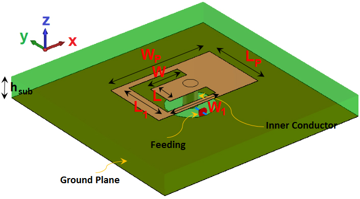
Figure 1: Transparent schematic of the antenna.
The essential parameters for designing a probe-fed printed patch antenna are: operation frequency (f), thickness, and dielectric constant of the employed substrate [9]. The selected resonant frequency for theproposed antenna design is 18 GHz (lower resonance frequency). Hence, the essential parameters of the dual-band patch antenna design are: f = 18 GHz, = 2.2 and h = 0.787 mm. The width of the patch can be given by:
| (1) |
where C, , and f are the speed of light, the dielectric constant (permittivity) of the substrate, and the desired resonant frequency, respectively. For a rectangular microstrip antenna, the value of the effective permittivity () can be calculated using:
| (2) |
Table 1: Parameter values of the antenna
| Parameter | W | L | h | W | L |
| Value (mm) | 55 | 110 | 0.787 | 4.32 | 2.5 |
| Parameter | W | L | W | L | W |
| Value (mm) | 4.32 | 2.5 | 4 | 1.5 | 3 |
| Parameter | L | W | W | L | d |
| Value (mm) | 2.25 | 4 | 3 | 2 | 0.8 |
| Parameter | d | d | d | d | d |
| Value (mm) | 1.72 | 4 | 0.5 | 1.7 | 4 |
The overall size of the radiation patch along its length is extended on each end by a distance L, which can be given by:
| (3) |
where h is the substrate height and W is the substrate width. For the resonant, the effective length is:
| (4) |
Then, the length of the patch resonator can be calculated as follows:
| (5) |
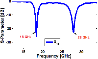
The final step of the dual-band patch antenna design is choosing the length of the second resonator element. By cutting a C-shaped slot at the antenna radiating patch, the second resonance at the higher frequencies (28 GHz) is generated. In the proposed design, the optimized length L is set to resonate at 0.25, where . corresponds to the second resonance frequency (28 GHz). The S result of the proposed antenna simulated using CST software [10] is illustrated in Figure 2(a), (b). As illustrated, using the proposed design, a good dual-band function with improved bandwidth has been achieved.
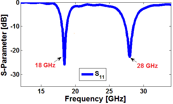
Figure 2: Simulated S of the dual-band patch antenna.
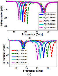
The simulated S curves of the proposed dual-band patch antenna for different values of radiation patch length (W) are plotted in Figure 3 (a). As seen, when the length of the radiation patch (main radiator) increases from 3.5 to 4.5 mm, the center of the first resonance decreases from 21 to 16 GHz. Based on this result we can conclude that the first resonance can be adjusted by changing the length of the main radiator (patch). Another important parameter of the proposed dual-band design is the C-shaped slot. The main effect of this structure occurs on the second resonance. In the proposed structure, the length of W is the critical parameter to control the upper operation band. Figure 3 (b) shows the simulated S results of the dual-band antenna with different lengths of W. As the width of the C-shaped slot changes from 1.5 to 2.5 mm, the operation frequency of the second resonance is varied from 25 to 32 GHz. Therefore, the operation frequency of second-resonance is tunable by changing the size of the embedded C-shaped slot.
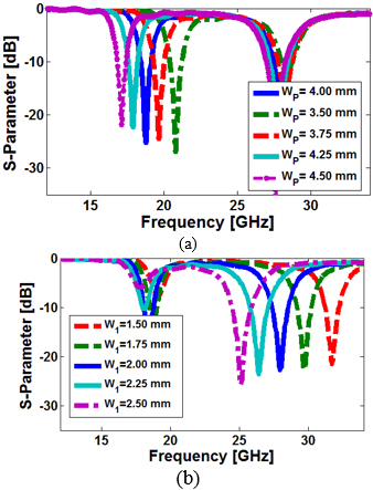
Figure 3: Simulated S for values of (a) W and (b) W.
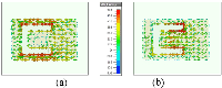
In order to realize the phenomenon for the dual-band performance of the antenna, the current distributions of the dual-band antenna at 18 and 28 GHz are depicted in Figure 4. As seen, at the first frequency (18 GHz), the current is concentrated on the edge regions of the rectangular radiating patch. Therefore, due to the resonant characteristics of the rectangular patch length, the impedance of the antenna can be tuned at this frequency [10]. As illustrated in Figure 4 (b), at the upper resonance frequency (28 GHz), the currents flow mainly around the modified C-shaped slot structure and justify the impact of the embedded slot on the generation of the second resonance. The simulated radiation patterns at 18 and 28 GHz are represented in Figure 5. As can be seen, the antenna provides a good radiation behavior in both of the operation frequencies. In addition, sufficient realized gains (more than 6 dB) are obtained for the designed dual-band antenna at the operation bands. The antenna element is fabricated and its return loss characteristics are measured. Figure 6 (a) illustrates the fabricated prototype. The measured and simulated S characteristic of the antenna are illustrated in Figure 6 (b). As seen, the antenna provides a dual-band performance around 18 and 28 GHz.
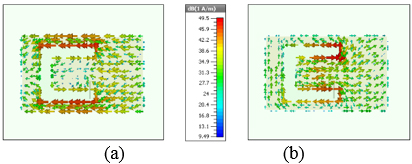
Figure 4: Current densities at (a) 18 GHz and (b) 28 GHz.
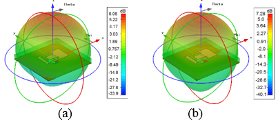
Figure 5: 3D radiations at (a) 18 GHz and (b) 28 GHz.
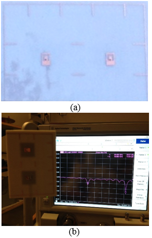
Figure 6: (a) Top view of the fabricated antenna elements and (b) measured/simulated S of the single antenna.
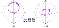
Figure 7 (a), (b) depicts polar views of the antenna radiation patterns including both, the co-polarized and cross-polarized, x-z plane (E-plane) and y-z plane (H-plane), respectively. As illustrated, the antenna has good radiation performance with stable co-polarization and low-level cross polarization. Furthermore, as can be seen, the effect of the probe feeding on the field pattern shapes at different operation frequencies is insignificant.
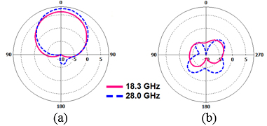
Figure 7: Simulated 2D radiation patterns of the dual-band antenna, (a) co-polarization, (b) cross-polarization.
The dual-band patch antenna maximum gain, and its efficiencies (radiation and total) over the operation frequency range are shown in Figure 8. In theory, the antenna efficiencies are related according to:
| (6) |
and the gain of the radiator can be calculated using the total efficiency and the directivity as follows:
| (7) |
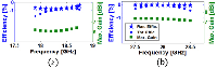
where e is the total efficiency of the antenna, er is the reflection efficiency = , eis the radiation efficiency, and D is the antenna directivity [11]. As can be seen from Figure 8, the antenna has desirable radiation properties with more than 6 and 7 dBi maximum gains at lower and upper operation frequencies, respectively. Furthermore, the antenna has a high-efficiency function at the frequencies of the antenna operation bands.
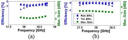
Figure 8: Simulated efficiencies and maximum gains of the antenna at, (a) lower and (b) upper operation bands.

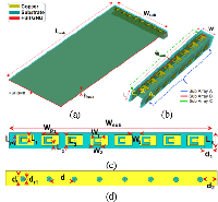
Figure 9: (a) Side view of the proposed mobile phone antenna, (b) antenna package configuration, (c) top and (d) bottom layers of each sub-array.
III. PROPERTIES OF THE 5G MOBILE PHONE PHASED ARRAY ANTENNA
The schematic of the presented 5G array antenna is illustrated in Figure 9. The design is composed of three dual-band patch antenna sub-arrays deployed at different edge regions of smartphone PCB. Eight elements of dual-band microstrip patch antennas are used for each sub-array. For the proposed design is the guided wavelength at the middle frequency (23 GHz). As can be observed in Figure 9 (a), the compact antenna package (Fig. 9 (b)) is deployed at the edge side of the PCB. The proposed mobile-phone 5G antenna has a full ground plane. The antenna design has an overall dimension of WL=55110 mm.
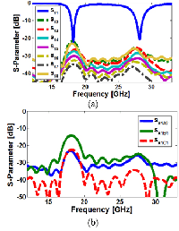
The simulated S-parameter of a single sub-array is illustrated in Figure 10 (a). As shown, the proposed phased array dual-band antenna provides good S-parameters with low mutual-couplings between antenna elements.
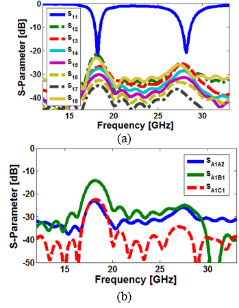
Figure 10: Simulated (a) S-parameters and (b) mutual-couplings of a sub-array.
Figure 10 (b) illustrates couplings among the antenna elements. The maximum mutual couplings between radiation elements of the design are occurred among “Antenna_A1-Antenna_A2,” “Antenna_A1-Antenna_B1,” and “Antenna_A1-Antenna_C1.” As illustrated, all of the mutual couplings are less than –25 dB, –13 dB, and –24 dB, respectively. It can be seen that the coupling between sub-array A elements and sub-array B elements are higher than the other couplings which occurred mainly because of the distance between two sub-array elements. As seen, the proposed antenna has good S-parameters and also it is not sensitive to the mutual coupling of the radiation elements.
Based on re-simulated results of the proposed design, it should be noted that the mutual coupling on an element within a sub-array when it is scanned and also the coupling between sub-arrays when one sub-array is scanned while monitoring coupling on an adjacent sub-array element have been investigated. According to the results, the antenna provides sufficient and low coupling between the elements and adjacent sub-arrays and its effects in the final conformal array is not significant to lead to a potential multi-path problem [12].
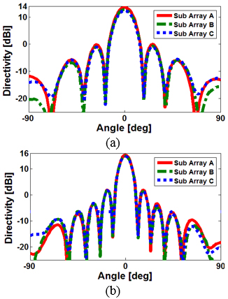
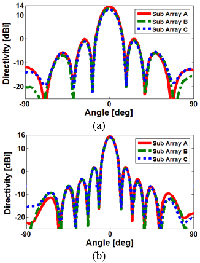
Figure 11: Directivities of the antenna at 0 for (a) 18 GHz, and (b) 28 GHz of operation bands.
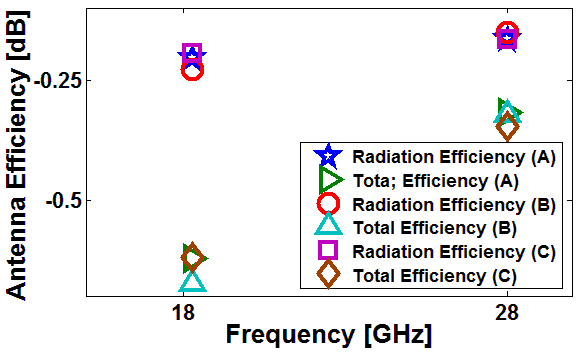
Figure 12: Simulated efficiencies of the different sub-arrays at 0 scanning angle.
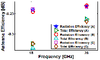
Figure 11 shows the simulated directivity characteristics of the dual-band design for sub-arrays at the main scanning angle (0). As illustrated, the antenna provides a good directivity property for all of the sub-arrays at 0. The antenna directivities for different sub-arrays are greater than 13.5 and 15.5 dBi at 18 and 28 GHz, respectively. The efficiencies (radiation and total) of the mobile phone antenna are illustrated in Figure 12. As shown, the antenna efficiencies are greater than –0.3 and –0.7 dB for radiation efficiency and total efficiency, respectively. From these results, it can be seen that the antenna provides good efficiencies at 18 and 28 GHz.
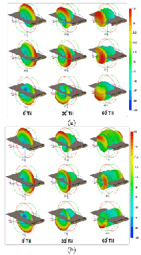
The 3D radiation beams of the proposed dual-band antenna array at 18 and 28 GHz for each sub-array are depicted in Figure 13 (a), (b), respectively. As seen, the proposed 3D beam coverage antenna package with the compact dual-band sub-arrays is highly effective to provide the required beam coverage for 5G handsets.
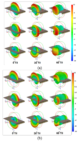
Figure 13: Radiation beams of each dual-band sub-arrays for different angles, (a) 18 GHz and (b) 28 GHz.
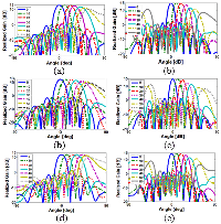
Figure 14 shows the 3D radiation beams of the dual-band antenna array at 18 and 28 GHz, respectively. As can be seen, the proposed dual-band antenna array provides a wide-scan beam steering function with the high gains for the scanning angles of 0, 30, and 60 degree. In the range of 0 to 30 degrees, the gain values are almost stable with the values of 13 dB at 18 GHz and 15 dB at 28 GHz. As shown, the sub-arrays possess relatively low side-lobe levels at the lower frequency (18 GHz). As illustrated, the side-lobe levels in the scanning range of 0 to 60 is less than 0 dB. However, as illustrated in Figure 14 at 28 GHz, the sub-arrays beams provided relatively high side lobes at the scanning degree 40 which is mainly because of the distance of the elements.
In general, the radiation-element distance should be chosen as /2 of the operation frequency [13, 14]. However, as the antenna provides dual-band function, it is difficult to achieve wide-scanning property at both operation frequencies. Therefore, high side-lobe levels will be appeared, especially at higher scanning angles of the lower frequency band.
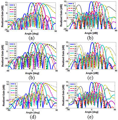
Figure 14: Simulated realized gains for, (a) sub-array A at 18, (b) sub-array B at 18, (c) sub-array C at 18, (d) sub-array A at 28, (e) sub-array B at 28, and (f) sub-array C at 28 GHz.
IV. CONCLUSION
The design and characteristics of a dual-band microstrip antenna array for 5G cellular communication systems is introduced in this paper. Three uniform linear eight-element dual-band patch antenna sub-arrays are used to achieve hemispherical radiation beams with 3D beam-coverage. The simulated result analysis of the proposed 5G antenna gives good fundamental properties in terms of impedance bandwidth, antenna gain/directivity, radiation pattern, and steering of the radiation beams. The obtained results show that the presented dual-band 5G antenna array could be used in the future 5G cellular communication systems. The proposed mobile phone phased array antenna is strongly effective to cover the required beam-coverage for 5G smartphones.
REFERENCES
[1] W. Roh, J. -Y. Seol, J. Park, B. Lee, J. Lee, Y. Kim, J. Cho, K. Cheun, and F. Aryanfar, “Millimeter-Wave beamforming as an enabling technology for 5G cellular communications: Theoretical feasibility and prototype results,” IEEE Commun. Mag., vol. 52, pp. 106–113, 2014.
[2] T. S. Rappaport, S. Sun, R. Mayzus, H. Zhao, Y. Azar, K. Wang, G. N. Wong, J. K. Schulz, M. Samimi, and F. Gutierrez, “Millimeter wave mobile communications for 5G cellular: It will work!” IEEE Access, vol. 1, pp. 335-349, 2013.
[3] Y. Wang, J. Li, L. Huang, Y. Jing, A. Georgakopoulos and P. Demestichas, “5G mobile: Spectrum broadening to higher-frequency bands to support high data rates,” IEEE Vehicular Technology Magazine, vol. 9, pp. 39-46, 2014.
[4] Y. Azar, G. N. Wong, K. Wang, R. Mayzus, J. K. Schulz, H. Zhao, F. Gutierrez, D. Hwang, T. S. Rappaport, “28 GHz propagation measurements for outdoor cellular communications using steerable beam antennas in New York city,” IEEE ICC, 2013.
[5] N. Ojaroudiparchin, M. Shen, and G. F. Pedersen, “Wide-scan phased array antenna fed by coax-to-microstriplines for 5G cell phones,” 21st International Conference on Microwave, Radar and Wireless Communications (MIKON), 2016.
[6] W. Hong, K. Baek, Y. Lee, and Y. G. Kim, “Design and analysis of a low-profile 28 GHz beam steering antenna solution for future 5G cellular applications,” IEEE International Microwave Symposium, 1-6 June, Tampa Bay, Florida, 2014.
[7] N. O. Parchin, Y. I. A. Al-Yasir, J. M. Noras, and R. A. Abd-Alhameed, “Dual-polarized MIMO antenna array design using miniaturized self-complementary structures for 5G smartphone applications,” EuCAP Conference, 31 March-5 April, Krakow, Poland, 2019.
[8] B. F. Wang and Y. T. Lo “Microstrip antenna for dual-frequency operation,” IEEE Trans. Antennas Propag., vol. AP-32, no. 9, pp. 938-943, 1984.
[9] C. A. Balanis, Antenna Theory Analysis and Design”, 3rd edition, Wiley, New Jersey, 2005.
[10] CST Microwave Studio, ver. 2020, CST, Framingham, MA, USA, 2020.
[11] R. Garg, P. Bhartia, I. Bahl, A. Itipiboon, Microstrip Antenna Design Handbook, Artech House, Boston – London, 2000.
[12] N. O. Parchin, R. A. Abd-Alhameed, and M. Shen, “Frequency-switchable patch antenna with parasitic ring load for 5G mobile terminals,” International Symposium on Antennas and Propagation (ISAP), Xi’an, China, 2019.
[13] A. Ullah, N. O. Parchin, R. A. Abd-Alhameed, and P. S. Excell, “Coplanar waveguide antenna with defected ground structure for 5G millimeter-wave communications,” IEEE MENACOMM, 19-21 Nov., Manama, Bahrain, 2019.
[14] N. O. Parchin, J. Zhang, R. A. Abd-Alhameed, G. F. Pedersen, and S. Zhang, “A planar dual-polarized phased array with broad bandwidth and quasi-endfire radiation for 5G mobile handsets,” IEEE Trans. Antennas Propag., vol. 69, pp. 6410-6419, 2021.
BIOGRAPHIES

Naser Ojaroudi Parchinis currently an assistant professor (lecturer) at Edinburgh Napier University, UK. He obtained his PhD in Electrical Engineering from University of Bradford, UK, where he was a Postdoctoral Research Assistant at the Faculty of Engineering and Informatics and worked as a research fellow in SATNEX V project, funded by European Space Agency. From 2018 to 2020, he was a Marie Curie Research Fellow in H2020-ITN-SECRET project funded by EU Commission. He is author and coauthor of several book chapters, and more than 300 technical journals and conference papers with more than 5200 citations and 40 h-index. His research interests include antennas, phased arrays, MIMO systems, microwave components, and electromagnetic wave propagation.

Osama M. Dardeerwas born in 1987. He received the B.S. degree with honor from Menofia University, Egypt, in 2009. He received the M.S. degree in electrical engineering from Ain Shams University, Egypt in 2017. He received the PhD degree in electrical engineering from Ain Shams University, Egypt in 2021. He is currently an Assistant Researcher at Microstrip Department, Electronics Research Institute, Egypt. He has been a member of research projects funded from national agencies such as National Telecommunication Regulatory Authority (NTRA). His research interests include UWB Antennas, Antennas for Mobile Generations, Band stop Filters, Radar Antenna Arrays, Power Dividers, RF Energy Harvesting, Internet of Things applications, and Optical Switching Networks.

Ahmed S. I. Amarreceived the B.S. degree in electrical engineering from the University of Alexandria, Alexandria, Egypt, in 2008, and the M.Sc. degree in electrical engineering from the Ain Shams University, Cairo, Egypt, in 2016. He is currently an Assistant Researcher at Electromagnetic Fields Department, ADR&D Center, Egypt, and aiming for getting a Ph.D. degree from Ain Shams University. His current research interests include Antennas, RF and Microwave Circuit Design, Power Amplifiers, and Millimeter-wave passive and active circuits Design.

Chan H. See received a first class B.Eng. Honours degree in Electronic, Telecommunication andComputer Engineering and a Ph.D. degree from the University of Bradford, UK. Currently, he is anAssociate Professor (Head of Electrical Engineering & Mathematics) in School of Engineering & the Built Environment, Edinburgh Napier University, UK. Previously, Mr. See was a Senior Lecturer (Programme Leader) in School of Engineering, University of Bolton, UK. His research interests cover wireless sensor network design, acoustic/microwave sensors, antennas and microwave circuits. He was awarded a certificate of excellence for his successful Knowledge Transfer Partnership (KTP) with Yorkshire Water in 2009. He has published over 110 journal articles and over 130 conference papers. He is a co-author for one book and five book chapters. Dr. See is a Chartered Engineer (CEng), Senior member IEEE, Fellow of the IET. He is also a Fellow of The FHEA, a full member of the EPSRC Review College, an Associate Editor for IEEE Access and an Editor for Peerj Computer Science, PLOS ONE and Wireless Power Transferjournals.

Raed Abd-Alhameed is a Professor of Electromagnetic and Radio Frequency Engineering at the University of Bradford, UK. He has long years’ research experience in the areas of Radio Frequency, Signal Processing, propagations, antennas and computational techniques, and has published over 800 academic journal and conference papers; in addition He is the Principal Investigator for several funded applications to EPSRCs and leader of several successful knowledge Transfer Programs He was awarded the business Innovation Award for his successful KTP with Pace and Datong companies on the design and implementation of MIMO sensor systems and antenna array design for service localizations. He is also a research visitor for Wrexham University, Wales covering the wireless and communications research areas. His interests are in 5G Green Communications Systems, computational methods and optimizations, wireless and Mobile communications, sensor design, EMC, MIMO systems, beam steering antennas, Energy efficient PAs, RF pre distorter design applications. He is the Fellow of the Institution of Engineering and Technology, Fellow of Higher Education Academy and a Chartered Engineer.
ACES JOURNAL, Vol. 36, No. 12, 1602–1609.
doi: 10.13052/2021.ACES.J.361212
© 2021 River Publishers