A Novel Dual-band Ambient RF Energy Harvesting System for Autonomous Wireless Sensor Node Application
Minh Thuy Le, Duc Anh Pham, Hong Tien Vu, Van Duc Ngo, and Quoc Cuong Nguyen
Department of Instrument and Industrial Informatics, School of Electrical Engineering
Hanoi University of Science & Technology, Hanoi 10000, Vietnam.
{thuy.leminh; cuong.nguyenquoc}@hust.edu.vn; {anhducbk.3i; vuhongtien98}@gmail.com; duc.ngo@hhd.vn;
Corresponding author: Quoc Cuong Nguyen (cuong.nguyenquoc@hust.edu.vn)
Submitted On: April 6, 2021; Accepted On: July 18, 2021
Abstract
This paper presents a novel dual-band ambient Wi-Fi energy harvesting system for an autonomous wireless sensor node (AWSN) which operates independently without other external power source. While conventional wireless sensor nodes are employing batteries with limited lifespans, an AWSN is supplied by harvested energy and does not require frequent battery replacement. Due to that reason, research on the energy harvesting aspect of AWSNs has been carried out intensively in recent years. By optimizing the matching network, the proposed ambient Wi-Fi energy harvesting system achieves a relatively good efficiency in dual-band at 2.45 GHz and 5.8 GHz. The efficiency reaches a peak at 47.45% and 42% at 2.45 GHz and 5.8 GHz, respectively. The proposed idea is numerically and experimentally demonstrated with the Wi-Fi source in building.
Index Terms: Ambient RF Energy Harvesting, Autonomous Wireless Sensor Node, Dual-band Rectenna.
I. INTRODUCTION
In recent years, rapid development of wireless sensor network promises a better change for life, it gives rise to many useful applications: water monitoring, animal monitoring, forest surveillance, pollution monitoring, and military system [1, 2]. In order to deploy the wireless sensor network (WSN) in real-life, there are many issues that need to be resolved like communication and information security, limited processing speed, reliability, latency, and especially the power source [3, 4]. To operating continuously, power supply for the sensor must be considered. Traditional power supply cords are not suitable due to immobility. Using batteries also has many disadvantages. The limited capacity of power source causes many problems such as short operating time, discontinuous data collection and transmission, maintenance costs, or even environment pollution caused by the batteries [5, 6]. Even though the lifetime of a sensor node can last to several years, thanks to the revolutionary development in low-power integrated circuit, there is always an expiration date and the battery will need to be recharged or replaced. For example, considering thousands of sensor nodes, covering a wide area up to several square miles. Collecting and replacing battery of one by one sin that case is nearly impossible and will dramatically increase the financial strain on operating the wireless sensor system. Furthermore, various applications of WSN are deployed in remote areas, such as forests, oceans, or on animal bodies, making any change and replacement difficult. To solve these issues, several energy harvesting techniques have been proposed as a battery replacement or an additional second power supply. Known as a potential solution for the problem, energy harvesting has the potential to make wireless sensor nodes completely autonomous [7].
Conventionally, there are various sources to harvest from. Heat from geothermal or from daily operation [8, 9], mechanical vibration [10, 11], solar energy [12, 13] and electromagnetics energy [14, 15, 16] are typical examples. Among these candidates, electromagnetic wave energy harvesting has been an especially promising direction. With the dramatic development of wireless communication system, the electromagnetic energy always exists in the ambient environment. Meanwhile, other sources such as heating, mechanical vibration, or solar energy are not always stable. RF energy harvesting utilizes the RF waves which readily exists in the ambient environment in the form of modulated signal such as Wi-Fi, GSM, 3G, 4G, and 5G with very low-input power (from -20 dBm to 0 dBm). In such RF energy harvesting systems, the most important component is rectenna. A rectenna consists of an antenna and a rectifying circuit. It was first invented by William C. Brown [17], inspired by various experiments of Nikolas Tesla about wireless power transfer [18]. Various research in RF power harvesting [19] have proved that harvesting and communicating can share the same set of antennas. However, low-power density of RF waves in the ambience leads to poor conversion efficiency from RF power to DC power. Consequently, pursuing high efficiencies is the highest priority for any research in rectenna design.
In recent years, efforts have been done to enhance the conversion efficiency [20], such as using spin diode and backward tunnel diode [21], optimizing based on signal waveform studies [22], harmonics processed [23], and eliminating the matching circuit [24]. In [25] and [26], the authors focused on the antenna designs to achieve complex impedances which matched with the input impedances of the rectifiers, eliminating the losses from matching circuit. This method enhances the conversion efficiency of rectenna and rectifier. However, the flexibility of this rectifier is limited and not suitable with the majority kinds of antenna which are mostly designed with 50 Ohm standard characteristic impedance.
In this study, for sensor nodes in building, the most suitable ambient RF source to harvest is the Wi-Fi at 2.45 GHz and 5.8 GHz which are ubiquitous and yield high-power density. This work proposes another method for adroitly eliminating matching circuit for loss reduction, by optimizing the geometry of each microstrip line in rectifier circuit, and to achieve 50 Ohm standard impedance. Section II presents the proposed dual-band rectifier and rectenna design as well as analysis. Section III provides the results and discussion for the fabricated and simulated structure compared with the related works. Finally, Section IV summarizes and concludes the paper.
II. DUAL-BAND RECTIFIER AND RECTENNA DESIGN
A common rectenna consists of three main parts: Antenna, Rectifier and Load, as shown in Figure 1. Rectenna firstly uses the antenna for receiving RF incident power from the environment. This power is then delivered to the Rectifier and converted to the DC power and consumed in the Load.
To evaluate a rectenna or rectifier, we need to consider how efficient the device can convert from RF power to useful DC power. The conversion efficiency η of the rectenna and rectifier is used for this purpose. For the rectifier, it is defined as the ratio of the output DC power and the input power of the rectifier, as shown in Equation (1):
| (1) |
where and are the output power and output voltage of the rectifier, is the load impedance, is the input power level of the rectifier.
For the rectenna, the conversion efficiency of a rectenna () is defined as the ratio of the output DC power and the incident power to the rectenna which is corresponding with the spectrum of RF power in the environment (), as shown in Equation (2):
| (2) |
where is the input power level of the rectenna that is corresponding with the radiated power from the Wi-Fi modem in the real test.
Fig. 1. Block diagram of a rectenna circuit.
A. Rectifier design
Rectifier is the most crucial part in a rectenna design. A common rectifier for RF energy harvesting consists of four main parts: RF Filter, impedance matching, AC to DC conversion block, and DC filter as in Figure 1. The most common rectifier structure is the half-wave rectifier (1 stage). This topology includes a single diode and one capacitor for charging and discharging. It is simple. Unfortunately, due to the power requirement on some applications, half-wave rectifier is not adequate. For this reason, the voltage doubler (2 stage), full-wave (3 stage) and multistage (4 stage) rectifiers are preferable due to higher output voltage. However, using more diodes increases the loss on each diode, reducing the total conversion efficiency of the circuit. Figure 2 presents the conversion efficiency of a rectifier at 2.45 GHz and 5.8 GHz corresponding to Wi-Fi based on IEEE 802.11.ac standard with different configurations. It should be noted that in this simulation, impact of power loss is investigated with configurations of the half-wave, voltage doubler, full-wave and multistage rectifier circuits using the same load with the same incident power level to choose the suitable rectifier configuration. The resistor of 1 k is used for the investigation. As observed, each topology will be only suitable for a specific range of input power. In the range of the input power from –10 dBm to 0 dBm, half-wave configuration can provide the highest conversion efficiency. However, as previously mentioned, voltage doubler can provide better output voltage, which is extremely important for supplying electronic devices operation. Therefore, to satisfy the requirements of conversion efficiency and adequate output voltage, voltage doubler configuration is chosen for the proposed design.
The key part of AC-DC block is the rectifying elements, which are usually Schottky diodes, transistors, and CMOS schemes [27]. All rectifier elements are nonlinear and can produce harmonic signals. As shown in [28], the amplitudes of harmonic signals significantly decrease the efficiency and the quality of output DC power. Thus, eliminating harmonic products is necessary for enhancing the efficiency of the whole rectenna.
Fig. 2. Simulated conversion efficiency of rectifying circuit at 2.45 GHz (a) and at 5.8 GHz (b) with different configurations (Load R = 1 k).
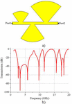
In the above fundamental rectifier structure, the capacitor positioned at the output also plays the role of a DC filter. However, this DC filter can only eliminate a small amount of harmonic products. Normally, DC filter based on microstrip technologies are preferred and is employed in this design. To achieve the good filter characteristic not only at 2.45 GHz and 5.8 GHz but also at their second and third harmonics, the proposed design uses three radial stub structures with different radii and open angles, as shown in Figure 3 (a). At the fundamental frequencies, the simulated insertion loss of the designed DC filter are 30.18 dB and 71.51 dB at 2.45 GHz and 5.8 GHz, respectively (Fig. 3 (b)). At the second and the third harmonics of 2.45 GHz, the insertion losses are 35.94 dB and 11.68 dB. For the 5.8 GHz, the designed filter achieves 31.05 dB and 33.52 dB insertion loss at the second and third harmonics, respectively. Due to the fact that the third harmonics have the least effect on the quality of the output [29], the insertion losses of the designed DC filter are suitable. The efficiency of DC filter will be proved by the total conversion efficiency of rectifier in the following contents of this section.
Fig. 3. The designed DC filter (a) and simulated transmission loss (b).
Fig. 4. The proposed rectifier.
To achieve as high conversion efficiency as possible, impedance matching network should be carefully studied. This work proposes a simple method to eliminating the matching circuit and enhancing the conversion efficiency. The input impedance of the rectifier is optimized with stub length variation which is connected to the shunted diode. Design progress can be summarized as follows:
Step 1. Design the DC filter covering fundamental and harmonic frequencies of 2.45 GHz and 5.8 GHz. The CST and Advanced System Design simulator are co-used for characterization of the DC filter’s performances.
Step 2. Design original rectifier following traditional method and observe the characteristic of design. In our design, we optimized original rectifier with the optimal load resistor of 3.9 k.
Step 3. Optimize the rectifier to achieve the best performance in conversion efficiency, by optimizing the geometry of each microstrip line in the AC to DC section. The major changes can be observed at the stub which connects the shunted diode to the main line. Geometrical dimensions of rectifier section (including the DC filter parameters) are listed in the Table 1.
The HSMS-2860 diode of Avago Technologies is used with low forward voltage (), low series resistance (). In general, the proposed design can achieve good efficiency and higher voltage than other earlier works. The detailed comparison of this work with previous works is given in the Table 2.
Table 1 Geometrical dimensions of entire proposed rectenna
| Parameter | L | L | L | L | W |
| Value(mm) | 5.2 | 1 | 3.5 | 8.4 | 1.1 |
| Parameter | W | W | W | W | R |
| Value (mm) | 1.1 | 0.63 | 1 | 1.5 | 6 |
| Parameter | R | R | |||
| Value (mm) | 10 | 12 | 70 | 70 | 80 |
| Parameter | R | R | L | L | W |
| Value (mm) | 17 | 23.2 | 15.9 | 15 | 2.4 |
Table 2: Comparison with the related works at the same input power level
| Ref. | Diode | Freq. | Eff. | Volt. | Size |
| (MHz) | (%) | (V) | ( x ) | ||
| [26] | SMS7630 | 2450 | 35 | N/A | N/A |
| [30] | SMS7630 | 1800 | 40 | 0.25 | 0.5 0.42 |
| 2450 | 33 | 0.22 | |||
| [31] | SMS7630 | 1800 | 25 | 0.3 | 0.3 0.3 |
| 2450 | 19 | 0.2 | 0.3 0.3 | ||
| [32] | SMS7630 | 950 | 31 | 0.3 | N/A |
| 1860 | 32 | 0.91 | |||
| [33] | HSMS2852 | 2450 | 45 | - | 0.6 0.73 |
| 5500 | 8 | ||||
| [34] | HSMS2860 | 24505000 | 12 | 0.352 | 0.97 x 0.68 |
| 4 | 0.174 | ||||
| This work | HSMS2860 | 2450 | 47.4* | 1.36* | 0.28 0.4* |
| 5800 | 42 | 1.28 | |||
| *The results of only rectifier in proposed structure. | |||||
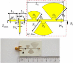
Fig. 5. The dual-band ring antenna in top (a) and bottom side (b).
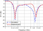
Fig. 6. Simulated and measured reflection coefficient.
B. Antenna design
Figure 5 presents the simple dual-band ring antenna which was designed for integration with the proposed rectifier. The total dimension of the antenna is 50 mm 35 mm, using RO4003C dielectric substrate with 3.5 relative permittivity and 0.0027 loss tangent.
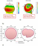
Designed antenna is experimentally investigated with a Keysight E5063A vector network analyzer. As can be observed in Figures 6 and 7, full-wave simulation and experimental results show a high agreement. Specifically, –10 dB measured impedance bandwidth is covered from 2.25 GHz to 2.75 GHz and from 5.45 GHz to 6.25 GHz. The omnidirectional radiation patterns of the dual-band antenna are presented in Figure 7, the antenna achieves the peak gain of 2.37 dBi and 4.26 dBi at 2.45 GHz and 5.8 GHz, respectively. Simulated and measured 2D radiation pattern of designed antenna at 2.45 and 5.8 GHz are shown in Figures 7 (b) and (c), respectively.
Fig. 7. 3D radiation pattern of the ring antenna (a), simulated and measured radiation pattern of the ring antenna at 2.45 GHz (b) and 5.8 GHz (c).
The proposed rectifier and rectenna was fabricated by the low-cost chemical etching system in RF3I laboratory, Hanoi University of Science and Technology (HUST).
III. EXPERIMENTS AND DISCUSSION
A. Measurement results
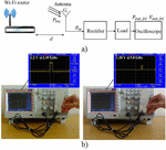
Figure 8 shows the image of the dual band rectenna prototype with the total dimension of 40 mm 103 mm. The measurement for harvested output voltage and conversion efficiency was performed in the building environment. Figure 9 (a) shows the measurement setup, which consists of three main parts: (1) RF source transmitter-Wi-Fi router, (2) rectenna, and (3) oscilloscope to measure the DC voltage at the load of the rectenna. To achieve different input power P, distance (d) between rectenna and Wi-Fi router are changed. The Wi-Fi signal radiated sources from a TP-link modem router in the building operates at two frequency bands 2.45 GHz and 5.8 GHz.
Fig. 8. The dual-band rectenna prototype: front (a) and bottom (b) view.
Fig. 9. Output voltage and conversion efficiency measurement setup using Wi-Fi TP-link modem in the building (a) and (b) actual rectenna DC output voltage measured by oscilloscope.
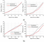
Fig. 10. Simulated and measured output voltage (a) and conversion efficiency (b) of the proposed rectifier.
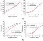
The resulted output voltage and conversion efficiency of rectifier and rectenna in simulation and measurement is compared in Figures 10 and 11. As observed, the simulated and measured results are agreeable.
For the rectifier case in Figure 10, the measurement of the proposed rectifier has been carried out with several antenna samples from RF3I laboratory. The proposed design achieves the best performances at 2.452 GHz and 5.745 GHz. In particular, at 2.452 GHz, the proposed rectifier achieves a 1.2 V output and 36.14% conversion efficiency in simulation, while in measurement, they are 1.28 V and 42%. Meanwhile, at 5.745 GHz, the output voltage and conversion efficiencies are 1.47 V and 54.26% in simulation and 1.36 V and 47.4% in measurement.
The similarity remains with the results of simulation and measurement of the proposed rectenna in Figure 11. At 2.452 GHz, the proposed rectenna achieves 1.21 V output and 34.03% conversion efficiency in simulation, while in measurement, these results are 0.77 V and 30.13%. At 5.745 GHz, the output voltage and rectenna conversion efficiencies are 1.46 V and 53.55% in simulation and 1.28 V and 42% in measurement. Obviously, both the output voltage and conversion efficiency of the proposed rectenna are smaller than these characteristics of the proposed rectifier. The main reason is on the difference of antenna used in the measurement. While the rectifier measurement was performed with several antennas which were specially designed for each desired frequency, the proposed rectenna uses a dual-band ring antenna, whose performances in gain, efficiency, and impedance bandwidth was carefully designed with various compromised. The harvested energy using the proposed rectenna is enough to go to the storage circuit which uses super-capacitors to power a wireless sensor node.
Fig. 11. Simulated and measured output voltage (a) and conversion efficiency (b) of the proposed rectenna.
B. Discussion
A comparison between the proposed structure and several previous works on rectenna and rectifier is presented in Table 2. As observed, compared to the previous works in [26] [30–33], the proposed structure has better efficiency, much higher output voltage, and more compact size. A plausible explanation is that the impedance matching circuit has been reduced in our work. Meanwhile, the earlier works employ multiple open stubs, shorted stubs, and radial stubs for this purpose [30] [32–34]. Even a simple matching circuit, such as a single inductor [31], can cause losses.
The proposed rectenna is suitable for practical applications. In real life situations, it can be equipped with a power management circuit. However, the integration of this circuit causes additional losses and lowers the overall efficiency [35]. This matter is reserved for future works.
IV. CONCLUSION
This paper proposed a dual-band rectenna for Wi-Fi energy harvesting system. The rectenna exhibited a 1.28 V output voltage and 42% conversion efficiency at 5.8 GHz and 0.77 V and 30.13% at 2.4 GHz from the in-building experiment. This amount harvested energy is enough for storage circuit which uses supercapacitors to power a wireless sensor node. Due to this advantage, the proposed rectenna can be used in practical application, such as supplying low-power wireless sensors. For that purpose, it has to be equipped with a proper power-management circuit, which not only stores the power but also boosts the output voltage to a suitable level, i.e., 3.3 VDC. This matter will be addressed in future works.
ACKNOWLEDGMENT
This research is funded by the Ministry of Education and Training (MOET) under grant number B2020- BKA-11.
REFERENCES
[1] R. J. M. Vullers, R. van Schaijk, H. J. Visser, and J. Penders, “Energy harvesting for autonomous wireless sensor networks,” IEEE Solid-State Circuits Magazine, vol. 2, no. 2, pp. 29-38, 2010.
[2] S. Zhang and H. Zhang, “A review of wireless sensor networks and its applications,” in 2012 IEEE International Conference on Automation and Logistics, Zhengzhou, China, pp. 386-389, Aug. 2012.
[3] C. Buratti, A. Conti, D. Dardari, and R. Verdone, “An overview on wireless sensor networks technology and evolution,” Sensors, vol. 9, no. 9, pp. 6869-6896, Aug. 2009.
[4] M. A. Matin and M. M. Islam, “Overview of wireless sensor network,” in Wireless Sensor Networks - Technology and Protocols, M. Matin, Ed. InTech, London, UK, 2012.
[5] N. H. Nguyen, T. D. Bui, A. D. Le, A. D. Pham, T. T. Nguyen, Q. C. Nguyen, and M. T. Le, “A novel wideband circularly polarized antenna for RF energy harvesting in wireless sensor nodes,” International Journal of Antennas and Propagation, vol. 2018, pp. 1-9, 2018.
[6] K. S. Adu-Manu, N. Adam, C. Tapparello, H. Ayatollahi, and W. Heinzelman, “Energy-harvesting wireless sensor networks (EH-WSNs): a review,” ACM Trans. Sen. Netw., vol. 14, no. 2, pp. 1-50, Jul. 2018.
[7] M. Magno, S. Sigrist, A. Gomez, L. Cavigelli, A. Libri, E. Popovici, and L. Benini, “SmarTEG: an autonomous wireless sensor node for high accuracy accelerometer-based monitoring,” Sensors, vol. 19, no. 12, p. 2747, Jun. 2019.
[8] M. Chen, H. Yu, G. Wang, and Y. Lian, “A batteryless single-inductor boost converter with 190 mV self-startup voltage for thermal energy harvesting over a wide temperature range,” IEEE Trans. Circuits Syst. II, vol. 66, no. 6, pp. 889-893, Jun. 2019.
[9] L. Hou, S. Tan, Z. Zhang, and N. W. Bergmann, “Thermal energy harvesting WSNs node for temperature monitoring in IIoT,” IEEE Access, vol. 6, pp. 35243-35249, 2018.
[10] L. A. J. Friedrich, J. J. H. Paulides, and E. A. Lomonova, “Modeling and Optimization of a Tubular Generator for Vibration Energy Harvesting Application,” IEEE Trans. Magn., vol. 53, no. 11, pp. 1-4, Nov. 2017.
[11] Z. Yang and J. Zu, “Toward harvesting vibration energy from multiple directions by a nonlinear compressive-mode piezoelectric transducer,” IEEE/ASME Trans. Mechatron., vol. 21, no. 3, pp. 1787-1791, Jun. 2016.
[12] Z. Chen, M.-K. Law, P.-I. Mak, and R. P. Martins, “A single-chip solar energy harvesting IC using integrated photodiodes for biomedical implant applications,” IEEE Trans. Biomed. Circuits Syst., vol. 11, no. 1, pp. 44-53, Feb. 2017.
[13] S. Mondal and R. Paily, “On-Chip Photovoltaic Power Harvesting System With Low-Overhead Adaptive MPPT for IoT Nodes,” IEEE Internet Things J., vol. 4, no. 5, pp. 1624-1633, Oct. 2017.
[14] Y. Zhang, S. Shen, C. Y. Chiu, and R. Murch, “Hybrid RF-solar energy harvesting systems utilizing transparent multiport micromeshed antennas,” IEEE Trans. Microwave Theory Techn., vol. 67, no. 11, pp. 4534-4546, Nov. 2019.
[15] J. Liu, K. Xiong, P. Fan, and Z. Zhong, “RF Energy Harvesting Wireless Powered Sensor Networks for Smart Cities,” IEEE Access, vol. 5, pp. 9348-9358, 2017.
[16] U. Muncuk, K. Alemdar, J. D. Sarode, and K. R. Chowdhury, “Multiband Ambient RF Energy Harvesting Circuit Design for Enabling Batteryless Sensors and IoT,” IEEE Internet Things J., vol. 5, no. 4, pp. 2700-2714, Aug. 2018.
[17] W. C. Brown, “The History of Power Transmission by Radio Waves,” IEEE Trans. Microwave Theory Techn., vol. 32, no. 9, pp. 1230-1242, Sep. 1984.
[18] K. Adachi, Radiant Energy: Unraveling Tesla’s Greatest Secret, Educate-Yourself.org, 2001.
[19] T. D. Ponnimbaduge Perera, D. N. K. Jayakody, S. K. Sharma, S. Chatzinotas, and J. Li, “Simultaneous wireless information and power transfer (SWIPT): recent advances and future challenges,” IEEE Commun. Surv. Tutorials, vol. 20, no. 1, pp. 264-302, 2018.
[20] Hucheng Sun, Yong-xin Guo, Miao He, and Zheng Zhong, “Design of a high-efficiency 2.45-GHz rectenna for low-input-power energy harvesting,” Antennas Wirel. Propag. Lett., vol. 11, pp. 929-932, 2012.
[21] C. H. P. Lorenz, S. Hemour, W. Li, Y. Xie, J. Gauthiers, P. Fay, and K. Wu , “Breaking the efficiency barrier for ambient microwave power harvesting with heterojunction backward tunnel diodes,” IEEE Trans. Microwave Theory Techn., vol. 63, no. 12, pp. 4544-4555, Dec. 2015.
[22] C. R. Valenta, M. M. Morys, and G. D. Durgin, “Theoretical Energy-Conversion Efficiency for Energy-Harvesting Circuits Under Power-Optimized Waveform Excitation,” IEEE Trans. Microwave Theory Techn., vol. 63, no. 5, pp. 1758-1767, May 2015.
[23] M. Roberg, T. Reveyrand, I. Ramos, E. A. Falkenstein, and Z. Popovic, “High-Efficiency Harmonically Terminated Diode and Transistor Rectifiers,” IEEE Trans. Microwave Theory Techn., vol. 60, no. 12, pp. 4043-4052, Dec. 2012.
[24] A. Lopez-Yela and D. Segovia-Vargas, “A triple-band bow-tie rectenna for RF energy harvesting without matching network,” in 2017 IEEE Wireless Power Transfer Conference (WPTC), Taipei, Taiwan, May 2017, pp. 1-4.
[25] T. S. Almoneef, “Design of a rectenna array without a matching network,” IEEE Access, vol. 8, pp. 109071-109079, 2020.
[26] C. Song, Y. Huang, J. Zhou, P. Carter, S. Yuan, Q. Xu, and Z. Fei, “Matching network elimination in broadband rectennas for high-efficiency wireless power transfer and energy harvesting,” IEEE Trans. Ind. Electron., vol. 64, no. 5, pp. 3950-3961, May 2017.
[27] L.-G. Tran, H.-K. Cha, and W.-T. Park, “RF power harvesting: a review on designing methodologies and applications,” Micro and Nano Syst Lett, vol. 5, no. 1, p. 14, Dec. 2017.
[28] J. Guo, H. Zhang, and X. Zhu, “Theoretical analysis of RF-DC conversion efficiency for class-F rectifiers,” IEEE Trans. Microwave Theory Techn., vol. 62, no. 4, pp. 977-985, Apr. 2014.
[29] S. Ladan and K. Wu, “Nonlinear modeling and harmonic recycling of millimeter-wave rectifier circuit,” IEEE Trans. Microwave Theory Techn., vol. 63, no. 3, pp. 937-944, Mar. 2015.
[30] S. Chandravanshi, K. K. Katare, and M. J. Akhtar, “A Flexible Dual-Band Rectenna With Full Azimuth Coverage,” IEEE Access, vol. 9, pp. 27476-27484, 2021.
[31] E. Vandelle, G. Ardila, S. Hemour, K. Wu, and T. P. Vuong, “Compact dual-band rectenna on a new paper substrate based on air-filled technology,” in 2019 IEEE Wireless Power Transfer Conference (WPTC), London, United Kingdom, pp. 307-311, Jun. 2019.
[32] S.-B. Liu, T. Ngo, and F.-S. Zhang, “Dual-band polarization-independent rectenna for RF energy harvesting,” in 2020 IEEE MTT-S International Microwave Workshop Series on Advanced Materials and Processes for RF and THz Applications (IMWS-AMP), Suzhou, China, pp. 1-3, Jul. 2020.
[33] M. Mattsson, C. I. Kolitsidas, and B. L. G. Jonsson, “Dual-band dual-polarized full-wave rectenna based on differential field sampling,” Antennas Wirel. Propag. Lett., vol. 17, no. 6, pp. 956-959, Jun. 2018.
[34] O. M. Dardeer, H. A. Elsadek, E. A. Abdallah, and H. M. Elhennawy, “A dual band circularly polarized rectenna for RF energy harvesting applications,” Applied Computational Electromagnetics Society (ACES) Journal, vol. 34, no. 10, pp. 1594-1600, Oct. 2019.
[35] X. Bai, J.-w. Zhang, L.-j. Xu, and B.-h. Zhao, “A broadband CPW fractal antenna for RF energy harvesting,” Applied Computational Electromagnetics Society (ACES) Journal, vol. 33. no. 5, pp. 482-487, May 2018.
BIOGRAPHIES

Minh Thuy Le received her engineering (2006), M.S. (2008) degree in Electrical Engineering from Hanoi University of Science and Technology and Ph.D. (2013) in Optique and Radio Frequency from Grenoble Institute of Technology, France. She is an assistant professor at the Department of Instrument and Industrial Informatics and also a Group leader of Radio Frequency group at Department of Instrumentation and Industrial Informatic (3I), School of Electrical Engineering (SEE), Hanoi University of Science and Technology (HUST). Her current interests include Antenna, Beamforming, Meta-materials, RF energy harvesting, indoor localization, and wireless sensors.

Duc Anh Pham was born in Stollberg, Germany, in 1994. He received his B.Eng. degree in Electrical Engineering from Hanoi University of Science and Technology (HUST), Hanoi, Vietnam, in 2017, and the M.S. degree in Microwave and Optics from the School of Electrical and Electronics Engineering, Chung-Ang University (CAU), Seoul, South Korea, in 2020.
From 2017 to 2018, he was an RF engineer with the Viettel Aerospace Institute, involved in researching and developing microwave circuits and systems for aerospace and defense industry. He is currently pursuing his Ph.D. with the School of Electrical and Electronics Engineering, Chung-Ang University (CAU), Seoul, South Korea. His research interests include millimeter-wave antennas, reconfigurable antennas, metasurfaced antennas, and RF energy harvesting.

Hong Tien Vu is currently a 5th-year student, major in Electrical Engineering, School of Electrical Engineering (SEE), Hanoi University of Science and Technology (HUST), Vietnam. His current interests include Antenna, Microwave circuits, and substrate integrated waveguide technology.

Van Duc Ngo was born in Ha Nam, Vietnam, in 1991. He received the B.Eng. degree and M.S. degree in Electrical Engineering from Hanoi University of Science and Technology (HUST), Hanoi, Vietnam, in 2014 and 2018, respectively. His research interests include design and analysis of antenna, RF energy harvesting, RF circuits/systems, and metamaterial.

Quoc Cuong Nguyen received his engineering (1996) and M.S. (1998) degrees in Electrical Engineering from Hanoi University of Science and Technology (HUST), Vietnam, and Ph.D. in Signal-Image-Speech-Telecoms from INP Grenoble, France, in 2002. He is a professor at the Department of Instrumentation and Industrial Informatics and also the head of Department of Instrumentation and Industrial Informatics, School of Electrical Engineering (SEE), Hanoi University of Science and Technology (HUST). His research interests include Signal Processing, Speech Recognition, Beamforming, Smart sensor, and RF communication.
ACES JOURNAL, Vol. 36, No. 10, 1367–1375.
doi: 10.13052/2021.ACES.J.361013
© 2021 River Publishers


