Equivalent Circuit Approximation to the Connector-Line Transition at High Frequencies using Two Microstrip Lines and Data Fitting
Duc Le, Nikta Pournoori, Lauri Sydänheimo, Leena Ukkonen, and Toni Björninen
1Faculty of Medicine and Health Technology
Tampere University, Tampere, Finland
duc.le, nikta.pournoori, lauri.sydanheimo, leena.ukkonen@tuni.fi
2Faculty of Information Technology and Communication Sciences
Tampere University, Tampere, Finland
toni.bjorninen@tuni.fi
Submitted On: September 24, 2021; Accepted On: December 7, 2021
Abstract
This article presents a method of obtaining an equivalent lumped element circuit to model the electrical connector-line transitions in the ultra-high frequency (UHF) band. First, the scattering matrices of two microstrip transmission lines that are otherwise identical but have the physical lengths of and are measured. Next, the theoretical model of the lines cascaded with the connector-line transitions modeled as lumped element circuits is established. The selection of the line lengths to be and results in an over determined system of equations that links the circuit component values to the two-port network parameters of the cascaded system. Finally, the least-squares data fitting procedure yields the best-fit component values. The results show that in our tested scenario, 3-component reactive circuit models well the transitions. Compared with the previous methods, the proposed approach does not require knowledge of the dielectric properties of the substrate of the measured transmission lines. This property integrates the method with our previous work on estimating a microstrip line substrate’s relative permittivity and loss tangent. The obtained transition circuit model is also validated through the testing of two quarter-wave transformers. The lines and transformers are implemented on a textile substrate to highlight the method’s applicability to wearable textile-based electronics.
Index Terms: microstrip line, electrical transitions, equivalent circuit, data fitting, least-squares method, over determined system, ABCD parameters, SMA connector, textile electronics.
I. INTRODUCTION
The research and development of high-frequency electronic and electromagnetic systems rely heavily on computer-aided engineering to predict and optimize their electrical response. In this process, the electrical responses are typically observed at the terminals that are internal to the modeled structure. In experiments, however, the signals are recorded through connectors. Although the physical distance to the system’s internal terminal through the connector is usually very short, its impact on the high-frequency signal transmission can be appreciable. The discontinuity in waveguide characteristics between the connector and the transmission line configuration internal to the system exacerbates the effect of this non-ideality further [1, 3].
Depending on the target application and the required precision of the numerical prediction of the system’s electrical response, the assumption that the connectors have a negligible impact on the high-frequency signal may be acceptable. Alternatively, the effect on the impedance matching, for instance, can be handled through post-manufacturing tuning. On the other hand, the connectors could be characterized with full-wave electromagnetic field simulations, but this is time-consuming and requires accurate knowledge of thestructure and materials of the connector.
Finally, the measurement-based de-embedding process could be used to characterize the connectors and subsequently remove their influence on the system’s electrical response. However, this requires custom-built test fixtures where the connector is mounted on and then measured with a vector network analyzer (VNA) under the conditions of various pre-determined terminations, such as short, open, and matched load. The terminations, however, are challenging to implement with highprecision at high frequencies over significant bandwidths. Moreover, the method is subject to the accuracy of the fixture characterizations, and in general, it is not straightforward to apply in practice [1, 2].
Recent literature proposes several approaches to more effectively characterize the electrical transitions due to connectors [2, 3, 4, 5, 6]. Most of the works ([2], [4, 5, 6]) incorporate simulations in the process of identifying the suitable model parameters that match the simulation outcome with the experiments. The authors of [5] used a semi-analytical approach tailored to the studied scenario of a Sub-Minature type A (SMA) connector, including a 90° corner. In the article [6], the authors considered a hybrid lumped-distributed circuit as a coupling model between a transverse electromagnetic (TEM) wave and two types of transmission lines. Still, they used a predefined numerical model of the entire SMA connector based on its structure and materials to account for its contribution to the electrical response. The article [2] presents a broadband model for the electrical transition through SMA connectors based on the cascade of several hybrid lumped-distributed circuits. However, the resources and expertise needed for the numerical optimization of the multi-stage circuit model and the implementation and testing of several fixtures aresignificant.
In contrast to the methods presented in [2], [4]–[6], the authors of [3] proposed a direct approach, which does not involve simulations or data fitting. The method is based on measuring two transmission lines of different lengths and using algebraic manipulations on the governing equation system comprising the cascade of the connectors and the lines to invert it. Consequently, they obtained the two-port network parameters for the electrical transitions due to the connectors. The method was demonstrated up to a notably high frequency of30 GHz.
However, similar to the works [2], [4]–[6], where the dielectric properties of the test structures need to be accurately known, the approach [3] requires the exact knowledge of the characteristic impedance and propagation constant of the transmission lines as a function of frequency. Still, they are not straightforwardly measured [7, 8]. Similarly, the measurement of the dielectric properties of materials at high frequencies remains a challenging task [9, 10]. As a result, with these approaches, significant time and effort must be dedicated to prior experiments, and combining the results with the characterization of the electrical transitions leads to the accumulation of uncertainty.
This article presents a new method of obtaining an equivalent circuit model to the connector-line transition and demonstrates it in the UHF band. Our method uses two transmission lines, but in contrast to the prior art, it is entirely independent of the EM properties of the materials involved in the lines. Therefore, the line width can be selected considering the ease of manufacturing, e.g., avoiding excessively narrow lines instead of optimizing the width to provide a particular characteristic impedance. These features make the method compelling for the emerging textile electronics applications, where the high-precision manufacturing and material characterization are even more challenging than the conventional high-frequency electronics applications [9–10]. The proposed method is simple to apply as it requires only the VNA measurement of two transmission lines and data fitting based on the well-known least-squares method. The fitting is based on basic circuit analysis considerations and does not involve circuit or EM fieldsimulations.
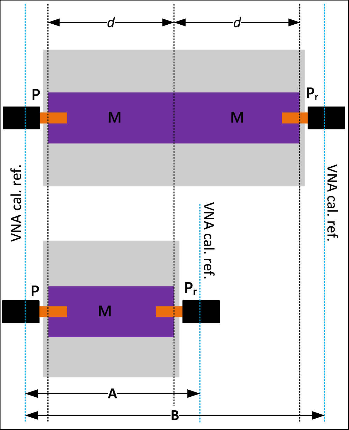
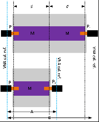
Figure 1: Top view of the microstrip line structures of the proposed two-line method. The boldface symbols denote the associated chain matrices used in the analysis.
II. METHOD
A. Data fitting approach
The method we propose for characterizing the connector-line transitions as lumped element equivalent circuits is two-fold. First, we implemented the two microstrip transmission line structures, MSL1 and MSL2 illustrated in Figure 1, and measured their two-port S-parameters with a VNA. Second, we performed the least-squares type model fitting for several circuit topologies to determine the type of the equivalent circuit and its component values that best represents the connector-line transitions. As illustrated in Figure 1, the two microstrip transmission line structures comprise identical RF connectors and the internal lines L1 and L2 with the respective physical lengths of and . All the other aspects of the lines, i.e., the substrate and conductor materials and the line widths, are equal. Importantly, we note that, in addition to this, no other properties, such as the substrate dielectric properties, need not be known. Overall, no numerical simulations are involved in the process.
For further analysis, we denote the chain (or ABCD) matrix of L1 as M so that using the cascading property of the chain parameters [11], [12, pp. 188–190], the chain matrix of L2 is given by the matrix product MM. Referring to Figure 1, we denote the chain matrix of the connector-to-line transition as . Given the assumption of identical connectors, we have for the chain matrix of the reverse, i.e., line-to-connector transition,
| (1) |
Thus,
| (2) |
from which we can solve
| (3) |
so that
| (4) |
Consequently,
| (5) |
This equation links the connector-line transition to the measured two-port network parameters of MSL1 and MSL2 through the matrix U.
Next, we note that M, P, and are reciprocal two-port networks because they are passive and are expected to comprise only regular bulk conductor and linear isotropic dielectric materials. Therefore, they exhibit determinants equal to one [11]. Moreover, since M is symmetric, A, B, and U are reciprocal and symmetric. Using these facts we obtain
and
The entry-wise comparison of the left- and right-hand sides of the matrix equation PP = U (eqn (5)) reveals that we can express three of the entries of P as functions of the fourth. However, the number of the independent equations does not suffice for solving all the elements of P. In other words, PP = U defines an over determined system of equations. By defining x P as a free variable and applying regular algebraic manipulations on the equation PP = U, we obtain
| (7) |
where x is an arbitrary non-zero complex number.
Because the connector-line transitions must be passive two-port networks, we hypothesize that they can be approximated as passive lumped element equivalent circuits over a range of frequencies. We denote the chain matrix modeling the forward, i.e., connector-to-line transition, as Q = (Q), i=1,2, j=1,2. Because we model the transition as a passive lumped element circuit, it is a reciprocal two-port network that satisfies det(Q) = 1 [11]. Consequently, an entry-wise inspection of the matrix equation P(x) = Q, where P(x) is given in eqn (7), yields four solutions for the variable x:
| (8) |
Ideally, for perfectly identical connectors, in the absence of any measurement uncertainty, and with a perfect agreement between the circuit model and reality, all four equations would yield the same solution for x. In practice, however, this is not possible. Therefore, we seek the component values that bring the four solutions as close as possible to each in the complex plane.
The centroid of the solution quadruplet is given by the mean value
| (9) |
where k is the frequency index in the list of N measured frequency points. Now, the least-squares type estimate for the solution can be obtained by identifying the set of circuit component values that minimizes the sum of the squared residuals defined as the sum of the squared distances from the centroid given by
| (10) | ||||
The implementation of the model fitting for particular circuit topologies will be discussed further in Section III
B. Preconditioning of the measured data
The initial assumption of our analysis is that MSL1 and MSL2 are symmetric two-port networks. Still, in practice this assumption cannot be satisfied precisely due to the measurement uncertainty and manufacturing tolerances. This non-ideality could lead to unexpected propagation of error through the governing system ofnon-linear equations. Therefore, we precondition the measured S-matrices of MSL1 and MSL2 by enforcing the symmetry condition (equal diagonal and anti-diagonal entries). Let and be the measured S-matrices of MSL1 and MSL2, respectively. Now, the entries of the corresponding symmetrized matrices can be estimated as the mean values of the relevant entries of the measured matrices
| (11) |
where i = 1,2. By using S and S as the source data for computing the corresponding chain matrices A and B for the model fitting procedure through the well-known two-port network parameter transformations [12, p. 192], the numerical values of the entries of U will necessarily follow the form defined in eqn (6c).
For assessing how much the symmetrized data differs from the original raw measured data at each frequency, we can inspect the value
| (12) |
where |||| denotes the matrix 2-norm [13, Ch. 2]. The larger the value, the better the initial symmetric network assumption holds in the original measured data. Thus, we can use this information to form weights for each frequency point in the model fitting. For this purpose, let N be the number of elements of a subset T of the measured frequency indices (1 N N) such that
| (13) |
By this definition, for a particular portion of the measured frequency points, we have t W. For example, if t = 15 and t = 20, and one would list W and W in the ascending order, then for more than N frequency points on the lists, W and W would take values greater than 15 and 20, respectively.
For the measured data that would fulfill the initial assumption of symmetric S-matrix very closely, t would take large values throughout the frequency range. Still, in practice t may also take very low values at some frequencies. Consequently, these frequencies should have proportionally less influence on the outcome of the model fitting. On the other hand, considering only the frequencies among the highest values of W would not be a balanced approach because it could over-emphasize the data from a limited sub-band of the total frequency range of interest in the model fitting. Given this, in the definition of t, we consider N to be rounded to the integer nearest to N/2. This way, considering at least half of the measured frequency points, if t t, then the measurement of MSL1 was in a relatively closer agreement with the initial assumption than MSL2, and vice versa.
Thus, we can first use the threshold numbers t and t, to compare for which one of the measured structures, the symmetrization yields smaller/larger deviation from the original data considering the whole frequency range. Second, with this information, we can compute the weighted average
| (14) |
which measures the fitness of the initial assumption of MSL1 and MSL2 both being symmetric two-port networks. This approach considers both structures but places proportionally more weight on the one for which the assumption holds true closer for 50% of the measured frequencies. Therefore, we can incorporate values W() as frequency weights in the computation of the sum of the squared residuals for the model fitting as
| (15) |
where, for simplicity, we have left out the multiplication with the constant scaling factor of 1/16 of the whole sum that appeared in the non-weighted eqn (10).
III. RESULTS FROM THE MODEL FITTING
A. Candidate circuit for the model fitting
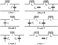
Transmission line theory establishes that over an infinitesimal length, a transmission line can be approximated as a lumped element equivalent circuit made up of series inductance and shunt capacitance [12, pp. 48–50]. The component values are determined by the structure and materials of the cross-section of the line. Series resistance and shunt conductance can be included in the model to account for the energy dissipation in the conductor and the dielectric material, respectively. Still, for electrically short lines, they are often negligible. Motivated by this and the fact that the connectors are certain types of transmission line or waveguide structures, we considered lumped element circuits that are combinations of series inductance and shunt capacitance as viable candidates to model the connector-to-line transition. In addition, we limit the study to the six cases listed in Figure 2, which are all the combinations of series inductance–shunt capacitance circuits with the number of components between two and four. The circuit for the reverse transition, i.e., line-to-connector, is obtained by reversing the order of the components.
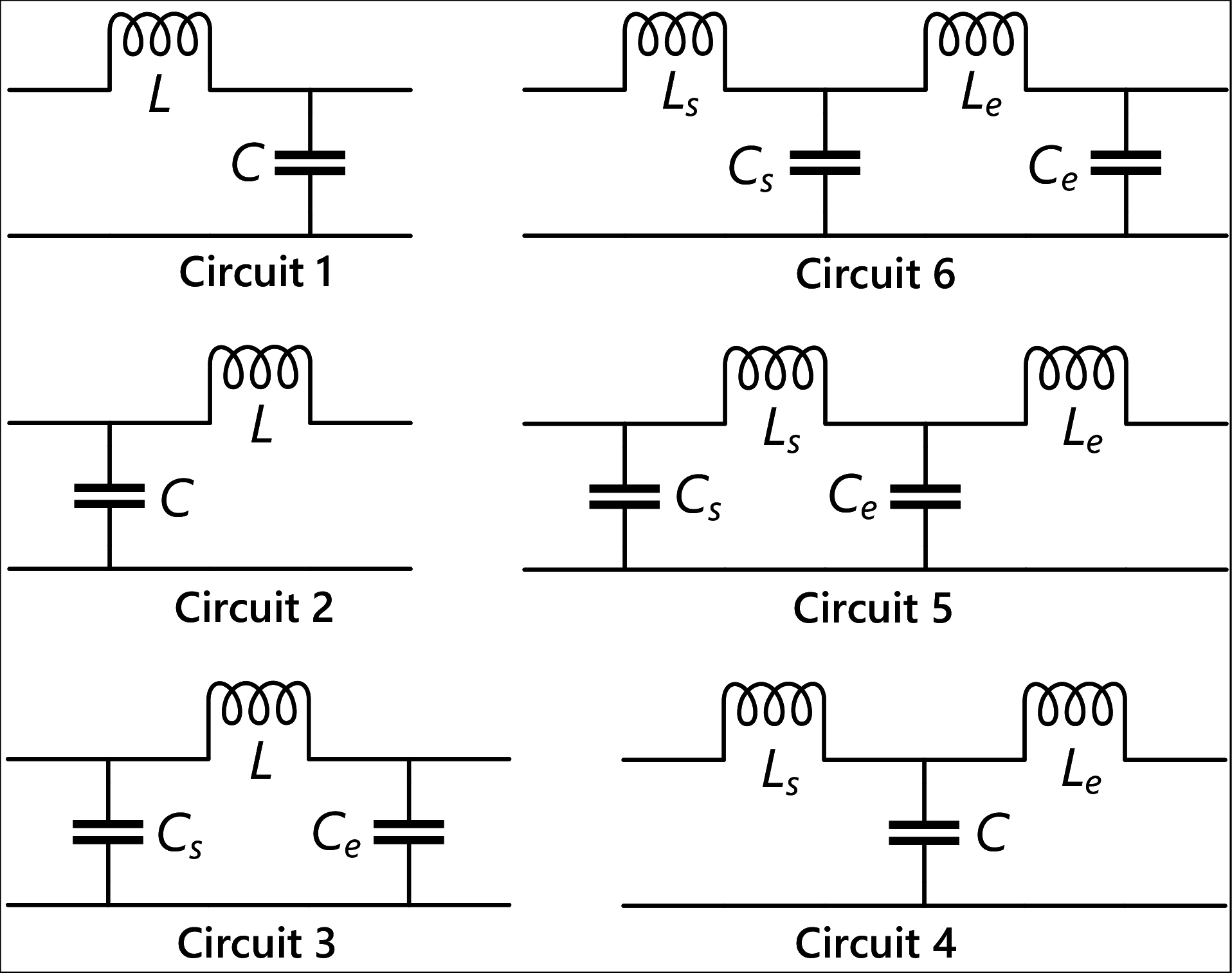
Figure 2: Circuits considered for modeling the connector-to-line transition. The connector is on the left and the line is on the right side of each circuit.
As an example, we derive here the chain matrix Q of Circuit 3 by cascading the three two-port networks representing shunt-connected capacitance C, series-connected inductance L, and shunt-connected capacitance C, in left-to-right order [12, p. 199]:
Regular algebraic manipulations yield
By substituting the elements of Q into eqn (8), we obtain
These are the four solutions for the variable x that will determine the sum of the squared residuals for any given circuit component values from eqn (15). The chain matrices of all considered circuits and the corresponding solution quadruplets for x are found analogously. We list them in Tables A.1 and A.2 in the Appendix.
B. Implementation and results
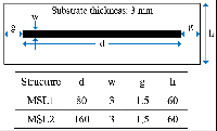
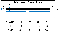
In this work, we targeted characterizing the connector-line transitions in the ultra-high frequency (UHF) range. For the experiments, we chose the frequency range from 800 MHz to 3 GHz. It covers several critical modern wireless applications, such as the UHF radio-frequency identification (RFID) at 866/915 MHz bands, L1-signal of the global positioning system (GPS) at 1575.42 MHz, and the industrial, scientific, and medical (ISM) band at 2.45 GHz. To highlight the fact that we do not need to know the electromagnetic properties of the line substrate for applying the proposed two-line method, we implemented the test structures MSL1 and MSL2 on textile type of material, ethylene-propylene-diene-monomer (EPDM) foam [14]. The connectors were SMA connectors used in the mounted-through configuration, i.e., the connectors’ body soldered to the ground plane and the center pin inserted through the substrate to the line terminal. Figure 3 shows the tested structures and their dimensions.
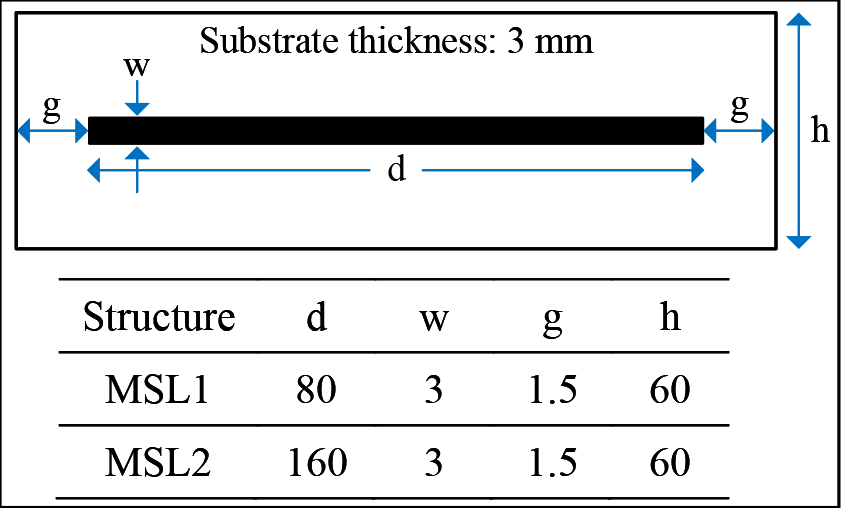
Figure 3: Top view of the microstrip line structures used in the measurement with the geometrical parameters reported in millimetres.
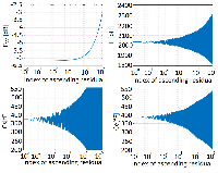
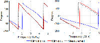
The S-parameter measurements were conducted with Keysight ENA Network Analyzer E5080A. For implementing the model fitting procedure, we used Mathworks MATLAB version R2018a. The search of the equivalent circuit component values that minimize the sum of the squared residuals was based on the direct computation of the residual given in eqn (15) over a uniformly spanned grid of the component values. The search was initiated considering the range of 0–800 fF and 0–2500 pH for the capacitors and inductors. Figure 4 illustrates the relationship between the component values and the residual error of the model fitting in the case of Circuit 3.
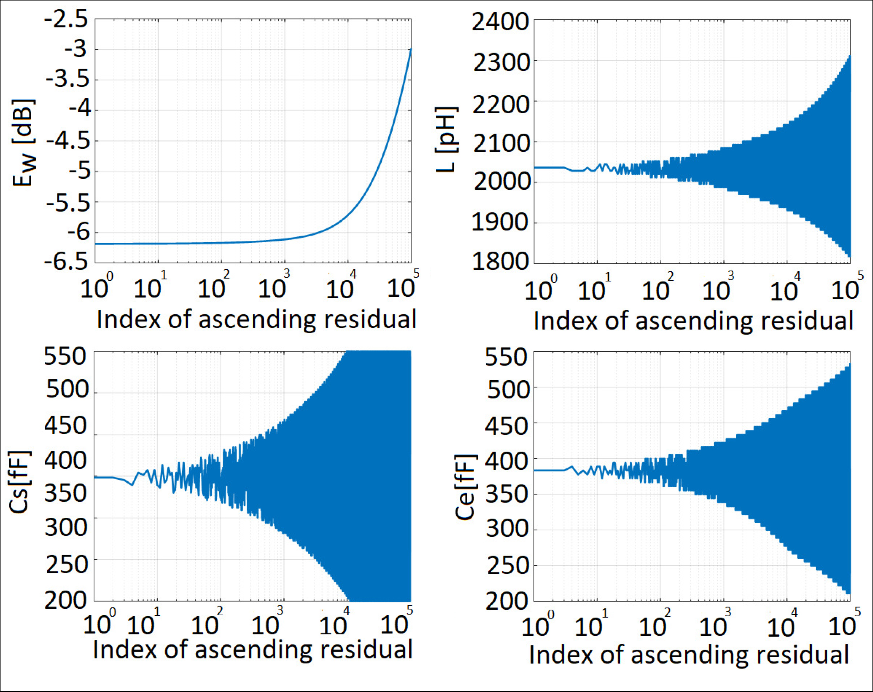
Figure 4: The residual (top left) from fitting the component values to Circuit 3 in the ascending order and the correspondingly ordered component values L, , and .
For the best 10,000 indices, E remains within 0.5 dB from the optimum. Thus, the fit is not highly sensitive toward the component values. The minimum-to-maximum variation of the component values for the best 10,000 induces are approximately 350 fF, 200 fF, and 300 pH, for C, C, and L, respectively. Comparison of the deviations relative to the optimum values indicates that the fit is most sensitive toward L and least sensitive toward C.
Table 1: Component values of the field circuits in [pH] and [fF]
| Circuit | L or | C or | [dB] | ||
|---|---|---|---|---|---|
| 1 | 3724 | 537 | N/A | N/A | 2.64 |
| 2 | 2131 | 964 | N/A | N/A | –0.4 |
| 3 | 2033 | 398 | N/A | 383 | –6.1 |
| 4 | 661 | 763 | 1383 | N/A | –5.5 |
| 5 | 2027 | 397 | 6 | 385 | –6.1 |
| 6 | 71 | 412 | 1973 | 368 | –6.1 |
Table 1 shows the outcome of the model fitting for all the studied circuits. The conclusions we draw from the results are summarized as follows:
- The residual for Circuits 1 and 2 is large compared with others.
- Circuit 4 achieved a notably smaller residual than Circuits 1 and 2 but higher than Circuits 3, 5, and 6.
- Circuits 3, 5, and 6 achieved low and nearly equal residuals.
- For Circuit 5, the value of the ending inductor is small. Thus, Circuit 5 is approximately Circuit 3.
- For Circuit 6, the value of the starting inductor is small. Thus, Circuit 6 is approximately Circuit 3.
Based on these observations, we conclude that Circuit 3 is the best choice for modeling the connector-line transitions for our studied microstrip line structures. Additionally, we note that our analysis converged to the same circuit topology adopted for a coaxial-to-microstrip transition by the authors of [3]. In the next section, we will demonstrate the applicability of the equivalent circuit in two microwave engineering scenarios.
VI. EXPERIMENTAL DEMONSTRATIONS
A. Estimation of the dielectric properties of the line substrate
In our previous work [10], we presented a method of estimating the frequency-dependent relative permittivity and loss tangent of the substrate of a microstrip transmission line. We did this by parameterizing the numerical simulation model of a transmission line as a function of these quantities, sweeping them over a range of values in the simulator, and then fitting the results to the measured data using the least-squares method. Since obtaining the equivalent circuit models for the connector-line transitions using the approach presented in this work does not require any prior knowledge of the dielectric properties of the substrate material, we can re-use the measured S-parameters of MSL1 and MSL2 for estimating the dielectric properties of the substrate material. This way, we can enhance the accuracy of our previous method [10] in two ways: first, by having the equivalent circuit models of the connector-line transitions, we can remove their parasitic contribution, and second, since we measure two lines as compared with a single one in [10], we can combine the data to reduce uncertainty.
The procedure described in Sections II and III provides the equivalent circuit models for the connector-to-line (chain matrix Q) and the reverse transition (chain matrix Q), such that we have and P Q in eqn (2). Thus, we obtain
| (18) |
which approximate the chain matrices of the transmission lines L1 and L2 internal to the measured structures MSL1 and MSL2 in Figure 1, respectively. Here A and B are the chain matrices corresponding with the symmetrized measured S-parameters of MSL1 and MSL2, respectively (eqn (11)).
Following the procedure described in [10], we sweep the values of the relative permittivity and loss tangent of the line substrate in a numerical simulation to find the values that provide the best fit between the simulation and measurement in the least-squares-sense. Moreover, the frequency-dependency of the relative permittivity and loss tangent will be defined by the Svensson/Djordjevic model based on the dielectric relaxation phenomenon [15, 16]. Thus, for parameterizing the simulation model, we sweep the values of the relative permittivity () and loss tangent (t), which define the dielectric properties of the substrate material at the given center frequency of the Svensson/Djordjevicmodel.
For most engineering applications, the critical features of transmission line circuits and components are the reflection coefficient, signal attenuation due to the internal power loss of the line given by the maximum attainable gain of the two-port network (G) [12, pp. 571–575], and the transmission phase angle. In this regard, at each frequency, we can define the following percentage differences
where the accent mark “” identifies the simulated quantities while the other quantities are derived from M and MM. Further, 1 k N is the frequency index, and i = 1,2 refers to L1 and L2, respectively. Any of these three percentage differences can be used to form the sum of squared residuals for the model fitting as
| (20) |
where i = 1,2 and m = 1,2,3. In eqn (20), the weights W computed from eqn (11) give relatively more importance to the frequencies where the initial assumption of the symmetric two-port network holds true closer in the original measured data.
To consider E, E and E simultaneously, we can combine them as the sum
| (21) |
where i = 1,2, and the three summands are normalized to their respective maxima over the considered model variations to uniformize their impact on the combined residual E. For each line, the pair of values and t that minimizes E is the least-squares estimate to the substrate material properties. However, for achieving a single estimate for and t, we can define the total residual E as the weighted average
| (22) |
which gives proportionally more weight to the data measured from the line that yields a smaller residual. The pair of values and t that minimizes E is the least-squares estimate to the substrate material properties at the center frequency of the Svensson/Djordjevic model with respect to the measured data from both lines.
We implemented the model fitting routine in Mathworks MATLAB version R2018a using Circuit 3 (Figure 2) with the component values listed in Table 1 to model the connector-line transitions. The frequency range we considered was from 800 MHz to 3 GHz, and the center frequency for the Svensson/Djordjevic dielectric relaxation model was set to 1 GHz. The transmission line simulations were performed using Keysight Advanced Design System (ADS) version 2013.06, where the relaxation model is internally implemented [17]. In the simulation, we swept and t over the intervals 1–3 (25 points) and 0.01–0.025 (20 points), respectively. The outcome is presented in Table 2 with a comparison to other works. Overall, the estimated values agree with the reported values in the literature. In comparison with our previous estimate [10], we note that removing the connector-line transitions through eqn (18) brought the estimated dielectric properties closer to the other works.
B. Computer-aided design and design verification of two quarter-wave transformers
Quarter-wave transformer is a typical passive transmission line component that transforms a given load resistance (R) to desired input resistance (R). It comprises a single transmission line section, which has an electrical length of 90 and the characteristic impedance of Z = [12, pp. 246–249]. Thus, optimizing the transformer requires accurate knowledge of the dielectric properties of the line substrate to enable finding the required physical width and length of the line that yields the targeted Z and the electrical length of 90. As an example, we considered transforming R = 50 R = 200 at 1 GHz and 2.45 GHz. For this transformation, we need Z = 100 .
Table 2: The dielectric properties of EPDM
| Reference | Frequency | Relative permittivity | Loss tangent |
| [10] | 1GHz | 1.534 | 0.01 |
| [18] | 900MHz | 1.23 | 0.02 |
| [19] | 868MHz | 1.21 | N/A |
| This work | 1GHz | 1.2821 | 0.0195 |
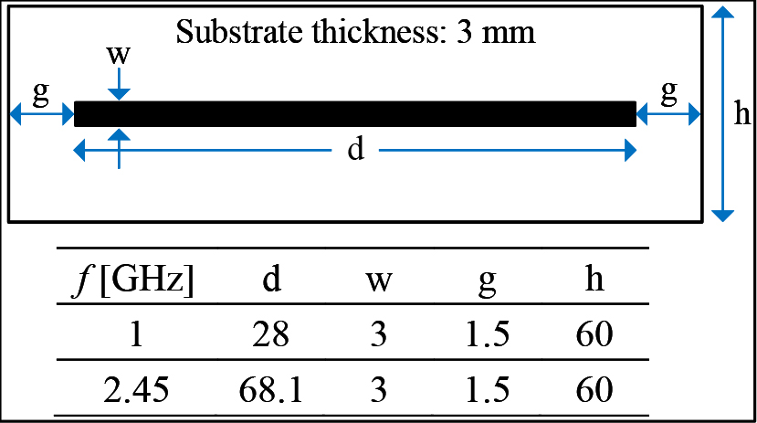
Figure 5: Top view of the implemented quarter-wave transformers with the geometrical parameters reported in millimeters.
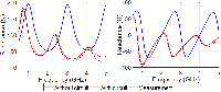
Next, we designed the transformers in Keysight Advanced Design System (ADS) version 2013.06 using the estimated dielectric properties of the substrate presented in the previous sub-section. Figure 5 shows the tested structures and their dimensions. Following the standard engineering practice, we optimized the transformers, excluding the connector-line transition circuits, and inspect their impact later by comparing the simulated and measured performance of the transformers. Figures 6 and 7 show the simulated and measured input impedance. The results show that the simulation without the connector-line transition circuits does not accurately predict the measured input impedance.
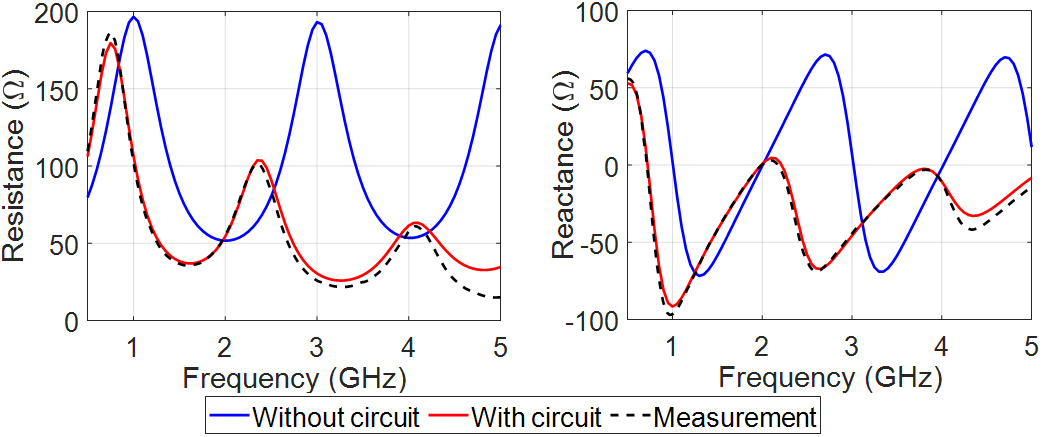
Figure 6: Input impedance of the quarter-wave transformer operating at 1 GHz.
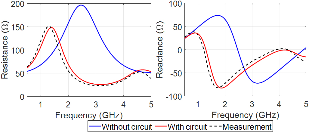
Figure 7: Input impedance of the quarter-wave transformer operating at 2.45 GHz.
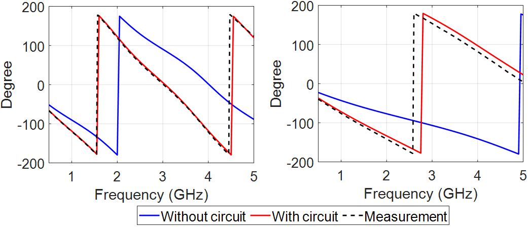
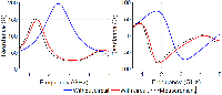
Figure 8: Electrical length of the quarter-wave operating at 1 GHz (left) and 2.45 GHz (right).
In contrast, the simulation, including the transition circuits, is in excellent agreement with the measurement. A similar conclusion holds for the measured electrical length of the transformers presented in Figure 8. Furthermore, the agreement in the results extends well beyond the frequency range of 800 MHz to 3 GHz, which was considered in the data fitting to obtain the transition circuit model and the dielectric properties of the substrate. Thus, we conclude that including the connector-line transition equivalent circuit in the simulation model notably improves the computer-aided design process and is readily applicable to the textile electronics application.
V. CONCLUSION
The VNA is a standard tool for the electrical characterization of high-frequency circuits and devices. Despite the device calibration, any residual physical separation between the VNA’s calibrated electrical contact point and the actual input terminal of the device under test causes a residual error in the measurement. We presented a new method of obtaining a lumped element equivalent circuit to model the electrical transition due to the connector. The method is based on the analysis and measurement of two microstrip transmission lines, one of which has precisely double the physical length of the other. It does not require knowledge of the dielectric properties of the line substrate or numerical simulations but relies on basic circuit analysis and the least-squares data fitting.
In the experiments, we found a 3-component reactive circuit to model well the electrical transition due to an SMA connector in a through mount configuration on a 3 mm thick textile substrate in the UHF band. Further, we applied the transition circuit model to augment our previously proposed method of estimating the relative permittivity and the loss tangent of the line substrate. Finally, we tested two quarter-wave transformers. The results showed that including the transition circuits in the computer-aided design process significantly improved the agreement between the simulated and measured results.
In our future work, we will consider replacing the transmission line as a test structure with a reconfigurable transmission line component to produce a larger set of data for the model fitting.
ACKNOWLEDGMENT
D. Le and T. Björninen were funded by Academy of Finland (funding decisions 294616 and 327789). N. Pournoori was funded by the Doctoral Programme in Biomedical Sciences and Engineering under the Faculty of Medicine and Health Technology of Tampere University. Additionally, D. Le was supported by Nokia Foundation, and N. Pournoori was supported by The Finnish Foundation for Technology Promotion (TES) and Nokia Foundation.
REFERENCES
[1] A. J. Lozano-Guerrero, F. J. Clemente-Fernandez, J. Monzo-Cabrera, J. L. Pedreno-Molina, and A. Diaz-Morcillo, “Precise evaluation of coaxial to waveguide transitions by means of inverse techniques,” IEEE Trans. Microw. Theory Techn., vol. 58, no. 1, pp. 229-235, Jan. 2010.
[2] T. Mandic, M. Magerl, and A. Baric, “Sequential buildup of broadband equivalent circuit model for low-cost SMA connectors,” IEEE Trans. Electromagn. Compatib., vol. 61, no. 1, pp. 242-250, Feb. 2019.
[3] R. Torres-Torres, G. Hernandez-Sosa, G. Romo, and A. Sánchez, “Characterization of electrical transitions using transmission line measurements,” IEEE Trans. Adv. Packag., vol. 32, no. 1, pp. 45-52, Feb. 2009.
[4] S. A. Wartenberg and Qing Huo Liu, “A coaxial-to-microstrip transition for multilayer substrates,” IEEE Trans. Microw. Theory Techn., vol. 52, no. 2, pp. 584-588, Feb. 2004.
[5] H. Zha, D. Lu, W. Wang, and F. Lin, “RF modeling and optimization of end-launch SMA to trace transition,” in Proc. IEEE Electronics Packaging and Technology Conference, Singapore, pp. 4,2015.
[6] T. Mandic, R. Gillon, B. Nauwelaers, and A. Baric, “Characterizing the TEM cell electric and magnetic field coupling to PCB transmission lines,” IEEE Trans Electromagn. Compatib., vol. 54, no. 5, pp. 976-985, Oct. 2012.
[7] J. A. Reynoso-Hernandez, “Unified method for determining the complex propagation constant of reflecting and nonreflecting transmission lines,” IEEE Microw. Wireless Compon. Lett., vol. 13, no. 8, pp. 351-353, Aug. 2003.
[8] R. B. Marks and D. F. Williams, “Characteristic impedance determination using propagation constant measurement,” IEEE Microw. Guided Wave Lett., vol. 1, no. 6, pp. 141-143, Jun. 1991.
[9] F. Declercq, H. Rogier, and C. Hertleer, “Permittivity and loss tangent characterization for garment antennas based on a new matrix-pencil two-line method,” IEEE Trans. Antennas Propag., vol. 56, no. 8, pp. 2548-2554, Aug. 2008.
[10] D. Le, Y. Kuang, L. Ukkonen, and T. Björninen, “Microstrip transmission line model fitting approach for characterization of textile materials as dielectrics and conductors for wearable electronics,” Int. J. Numerical Modelling Electronic. Netw., Dev. Fields, vol. 32, no. 6, pp. 10, Feb.2019.
[11] P. L. D. Peres, I. S. Bonatti, and A. Lopes, “Transmission line modeling: A circuit theory approach,” SIAM Review, vol. 40, no. 2, pp. 347-352, Jun. 1998.
[12] David M. Pozar, Microwave Engineering, 4th Ed., Hoboken, NJ, USA: Wiley, 2012.
[13] Gene. H. Golub, Matrix Computations, 2nd Ed., Baltimore, MD, USA: Johns Hopkins University Press, 1989.
[14] Johannes Birkenstock GmbH. Wuppertal, Germany. Available: http://www.johannes-birkenstock.de/index.html
[15] C. Svensson and G. E. Dermer, “Time domain modeling of lossy interconnects,” IEEE Trans. Adv. Packag., vol. 24, no. 2, pp. 191-196, May 2001.
[16] A. R. Djordjevic, R. M. Biljic, V. D. Likar-Smiljanic, and T. K. Sarkar, “Wideband frequency-domain characterization of FR-4 and time-domain causality,” IEEE Trans. Electromag. Compatib., vol. 43, no. 4, pp. 662-667, Nov. 2001.
[17] Keysight Technology, “About dielectric loss models,” Keysight Online Knowledge Center 2009. Available: http://edadocs.software.keysight.com/display/ads2009/Conductor+Loss+Models+in+Momentum.
[18] Koski K, Sydänheimo L, Rahmat‐Samii Y, and Ukkonen L, “Fundamental characteristics of electro‐textiles in wearable UHF RFID patch antennas for body‐centric sensing systems,” IEEE Trans. Antennas Propag., vol. 62, no. 12, pp. 6454-6462, Dec. 2014.
[19] S. Manzari, S. Pettinari, G. Marrocco, “Miniaturized and tunable wearable RFID tag for body‐centric applications,” in Proc. IEEE Int. Conf. RFID‐Technologies and Applications, Nice, Italy, 5-7 Nov. 2012, pp. 239-243.
APPENDIX
Table A.1: Chain matrices (Q) of the lumped element equivalent circuits listed in Figure 2
| Circuit 1 | |
|---|---|
| Circuit 2 | |
| Circuit 3 | |
| Circuit 4 | |
| Circuit 5 | |
| Circuit 6 |
Table A.2: Solution quadruplets to equation , where and Q are given in equation (7) and Table A.1
| Circ. 1 | ||
|---|---|---|
| Circ. 2 | ||
| Circ. 3 | ||
| Circ. 4 | ||
| Circ. 5 | ||
| Circ. 6 | ||
BIOGRAPHIES

Duc Lereceived the B.Sc. degree in electrical engineering from HCMC University of Technology and Education, Ho Chi Minh City, Vietnam, in 2014 with excellent degree and the M.Sc. degree with distinction in Electrical Engineering from Tampere University of Technology (TAU), Tampere, Finland, in 2018.
Currently, Mr. Le pursues a Ph.D. degree with the Faculty of Medicine and Health Technology, Tampere University, Tampere. His research interests include wireless health technology, wearable antennas, electromagnetic modeling, RF circuits, RFID tags, and low-profile antennas. Mr. Le is a recipient of prestigious awards, including HPY Research Foundation of Elisa and the Nokia Foundation Scholarship.

Nikta Pournoorireceived the M.Sc. degree in electrical engineering specializing in RF-electronics from the Tampere University of Technology, Tampere, Finland, with distinction in 2018.
Currently, she pursues a Ph.D. degree with the Faculty of Medicine and Health Technology, Tampere University, Tampere. Her research interests include implantable antenna design and sensors for biomedical telemetry systems, RF energy harvesting systems, wireless power transfer, and RFID systems. She is a recipient of prestigious awards, including the Nokia Foundation Scholarship and the Finnish Foundation for Technology Promotion (TES).

Lauri Sydänheimoreceived the M.Sc. and Ph.D. degrees in electrical engineering from the Tampere University of Technology (TUT), Tampere, Finland. He is currently a Professor with the Faculty of Medicine and Health Technology, Tampere University, Tampere, Finland. He has authored more than 250 publications in radio-frequency identification tag and reader antenna design and wireless system performance improvement. His current research interests include wireless data communication and wireless identification and sensing.

Leena Ukkonenreceived the M.Sc. and Ph.D. degrees in electrical engineering from the Tampere University of Technology, Tampere, Finland, in 2003 and 2006, respectively. She is currently a Professor with the Faculty of Medicine and Health Technology, Tampere University, Tampere, Finland, and is leading the Wireless Identification and Sensing Systems Research Group. She has authored more than 300 scientific publications in radio-frequency identification (RFID), antenna design, and biomedical and wearable sensors. Her current research interests include RFID antennas, RFID sensors, implantable biomedical systems, and wearable antennas.

Toni Björninenreceived the M.Sc. and Ph.D. degrees in electrical engineering from Tampere University of Technology (TUT), Tampere, Finland, in 2009 and 2012, respectively.
He works as a University Lecturer at the Faculty of Information Technology and Communication Sciences, Tampere University (TAU), Tampere, Finland. During 2013–2016 he held the post of Academy of Finland Postdoctoral Researcher at TUT and, subsequently, the Academy of Finland Research Fellow post during 2016–2021 at TUT and TAU. He has been a Visiting Postdoctoral Scholar in Berkeley Wireless Research Center at UC Berkeley and Microwave and Antenna Institute in Electronic Engineering Department at Tsinghua University, Beijing, China. Dr. Björninen’s research focuses on microwave technology for wireless health, including implantable and wearable antennas, wireless power transfer, sensors, and RFID-inspired wireless solutions. He is an author of 185 peer-reviewed scientific articles and a Senior Member of the IEEE.
Dr. Björninen serves as an Associate Editor in Applied Computational Electromagnetics Society Journal. Previously, he has been a member of the editorial boards of IEEE Journal of Radio Frequency Identification (2017–2020), IET Electronics Letters (2016–2018) and International Journal of Antennas and Propagation (2014–2018).
ACES JOURNAL, Vol. 36, No. 12, 1541–1551.
doi: 10.13052/2021.ACES.J.361205
© 2021 River Publishers