Design of Planar Directional Coupler using 2-Bit Fragment Structures
Yonghui Tao, Wenjuan Zhang, Johan Sidén, and Gang Wang
1Department of Electronic and Information Engineering
Jinling Institute of Technology, Nanjing, 211169, China
yhtao87@jit.edu.cn
2Department of Electronic Engineering and Information Science
University of Science and Technology of China, Hefei, 230027, China
Antenna Design University, City, State Code Zip Code, Country
gwang01@ustc.edu.cn
wjz16@mail.ustc.edu.cn
3Department of Electronics Design
Mid Sweden University, SE-851 70 Sundsvall, Sweden
Johan.Siden@miun.se
Submitted On: September 2, 2021; Accepted On: November 4, 2021
Abstract
Automatic design of planar directional coupler can be implemented by multi-objective optimization searching for the optimal planar fragment-type structure (FTS). The 2-bit FTS description scheme may include necessary fine structures in fragments to enhance the FTS design. By coding the coupler design space on PCB in 2-bit FTS, defining the FTS design matrix, and searching for the optimal structure, directional coupler can be designed without any structure presetting or artificial intervention. The scheme is demonstrated by designing 10-dB wideband directional coupler with 2-bit FTS scheme. The designed directional couplers are fabricated and tested to show maximum directivity of 58 dB with 36% operation bandwidth.
Index Terms: directional coupler, fragment-type, directivity, modeling, optimization.
I. INTRODUCTION
Microstrip directional couplers are widely used in RF/microwave systems. Traditional microstrip directional couplers are based on coupled lines, which have limited directivity and bandwidth due to the phase velocity difference between the odd and even modes [1].
In order to improve the directivity and bandwidth, different design techniques have been proposed to seek more appropriate coupler structure. Based on the idea of distributed compensation, planar artificial transmission lines [2] and lumped elements [3, 4, 5] have been used to enhance the coupler performance, and generate directivity higher than 20 dB. Multilayer structure is proposed in [6] to improve the minimum directivity to 20 dB over a bandwidth of 10% for coupling of 14.3 dB. A 10-dB directivity-enhanced coupler is designed in [7] by using epsilon negative transmission line, which yields a directivity above 20 dB in a bandwidth of 8.7%. A 15-dB coupler of directivity higher than 22 dB is designed in [8] by using multiple narrow strips and an open slot on the ground. Asymmetric multi-section stripline is proposed in [9] to improve the minimum directivity to 25 dB over a bandwidth of 55% for 18.5 dB coupling. A 10-dB coupler using multi-mode resonator is reported in [10] to present a minimum directivity of 25 dB within a bandwidth of 24%. Periodic metallic cylinders are set on microstrip lines to design 12dB coupler of directivity of 46 dB in [11]. For all these designs, canonical structures of certain types play important roles in the coupler designs.
Recently, a design scheme by using fragment-type structure (FTS) is proposed in [12] to challenge the high directivity and broad bandwidth. The FTS-based planar directional coupler presents a minimum directivity of 37 dB in a relative bandwidth of 45% for 20 dB coupling, and directivity of 28.7 dB in 29% bandwidth for 10 dB coupling [12]. In the FTS designs, appropriate narrow slots are preset to ensure efficient searching for the optimal FTS structure to define the coupler.
To improve the design performance and optimization efficiency, 2-bit FTS has been considered in planar low-pass filter design [13]. It is shown that the design of low-pass filter with the 2-bit FTS elements can acquire higher roll-off rate, wider stopband width, and higher stopband suppression with shorter optimization time, if compared with the design using conventional 1-bit FTS scheme.
In this paper, 2-bit FTS design scheme is proposed for automatic design of high-performance microstrip directional coupler. The appropriate 2-bit FTS elements for directional coupler, the coding for the enhanced FTS design matrixes, and the multi-objective optimization searching for the optimal FTS directional couplers are presented in Section II. In Section III, the proposed 2-bit FTS scheme is demonstrated by challenging the 20 dB and 10 dB planar directional couplers.
II. MULTI-OBJECTIVE OPTIMIZATION SCHEME FOR FTS-BASED DIRECTIONAL COUPLER
With no loss of generality, we consider a design space of dimensions ab on PCB for directional coupler. Suppose the design space is to be discretized into cells of dimensions wl, the design space is gridded into cells of number of mn=(a/w)(b/l).
When 2-bit FTS is used for high performance design, appropriate fine or subtle structures on FTS elements are required.
A. Structure description with 2-bit FTS
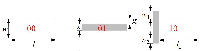
For planar directional coupler, we may choose the 2-bit FTS elements as shown in Figure 1, where two of the FTS elements bear thin metal lines of the width s in vertical and horizontal directions, respectively. By assigning binary codes 00, 01, 10, and 11 to different elements, the 2-bit FTS can be coded.
For the 2-bit FTS elements, different thin lines and slots can be defined by setting different fine structure parameters g and s. The vertical thin line in element “10” is set to extend outside the cell in y-axis direction by wand w, which ensure the connection with the adjacent cell “01.” The gap coupling can be formed between adjacent cells “01” and “11.” Note that the line width s may be set according to the machining precision for PCB processing. In the following design, it is set as s = 0.2 mm.
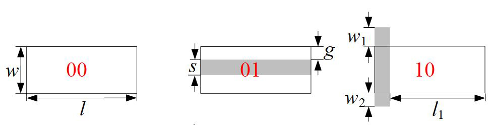
Figure 1: Elements proposed for the 2-bit FTS scheme.
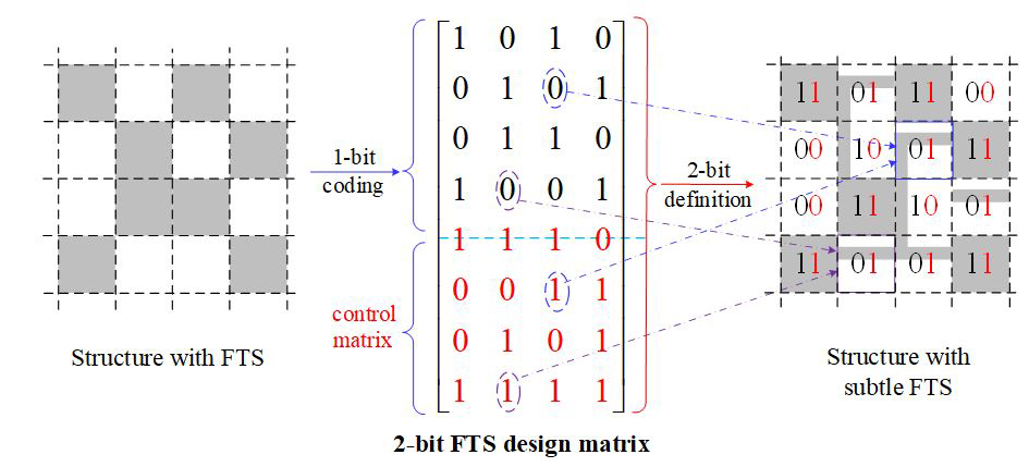
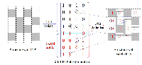
Figure 2: Structure coding for the 2-bit FTS scheme.
Figure 2 shows the structure coding for the 2-bit FTS description by combining the 1-bit FTS coding and a control matrix, which can be implemented in the following steps:
- Discretize the space on PCB reserved for the coupler.
- Assign every cell with either “0” or “1” to form the 1-bit matrix, where “1” = metal and “0” = empty.
- Assign control code “1” or “0” to the 1-bit codes, to form the 2-bit coding: “11” = full metal, “10”=vertical thin line, “01”=horizontal thin line, “00”=empty.
- Define a control matrix with the control code “1” and “0”.
- Combine the 1-bit design matrix and the control matrix to yield the 2-bit FTS design matrix.
The above 2-bit coding scheme clearly shows that the 2-bit FTS design matrix is always twice the 1-bit design matrix. To include the same thin lines and gaps with the conventional 1-bit scheme, it will need a design matrix enlarged at least to the size of (w/s)(l/s), which could be a huge and impractical decision space for multi-objective optimization searching.
B. Objective functions for MOEA/D-GO
Multi-objective optimization searching can be used for design of high-performance planar directional coupler. The specifications of a directional coupler, such as coupling level, return loss (RL) and isolation, can be set as the key indicators for optimization. The objective functions for a directional coupler can be specified as follows [12]:
| (1) |
| (2) |
| (3) |
| (4) |
| (5) |
where [, ] defines the desired band of the microstrip directional coupler, |S| indicates the coupling level, |S| indicates the isolation, and |S| indicates the return loss (RL).
Objective function f(x) guarantees a coupling level of C (in dB) in the desired band. The objective function f(x) ensures the stability of coupling level, and is the maximum allowable fluctuation of coupling level. Objective function f(x) controls the desired isolation is greater than Q (in dB). Objective function f(x) ensures that RL is greater than R (in dB). Objective function f(x) assures the operation bandwidth, denotes the center frequency and BW is the desired fractional bandwidth.
With the above defined objective functions, the decision matrix for FTS can be optimized to yield the optimal coupler structure. The multi-objective evolutionary algorithm based on decomposition combined with enhanced genetic operators (MOEA/D-GO) for 2-bit FTS [13] can be used to search for the optimal design matrix.
III. COUPLER DESIGNS WITH 2-BIT FTS
For demonstration, the directional coupler is supposed to be printed on a PCB of FR4 substrate ( = 4.4, tan = 0.02) and thickness of 1.6 mm. The design space on PCB is 10.3 mm 16.4 mm. In addition, the coupler structure on PCB is supposed to have both the horizontal and vertical symmetry so that the real design space for FTS optimization searching is 5.15 mm 8.2 mm.
For FTS modeling, the design space 5.15 mm 8.2 mm is discretized into 12 6 cells so that the 2-bit FTS scheme needs a design matrix of 12 12, in which 12 6 matrix is the control matrix, as shown in Figure 2.
The parameters defining the 2-bit FTS elements in the Figure 2 are: w = 0.44 mm, l = 1.54 mm, l = 1.34 mm, s = 0.2 mm, g = 0.1 mm, w = 0.34 mm and w = 0.3 mm. By setting w = 0.44 mm and l = 1.54 mm, necessary overlap between the adjacent cells can be guaranteed for side or diagonal connection. In addition, g = 0.1 mm ensures a small gap can be yielded.
A. Design of 20-dB directional coupler
For the 20-dB directional coupler, the design objectives are set with C = 20 dB in eqn (1), with = 0.5 in eqn (2), Q = 70 in eqn (3), R = 40 in eqn (4), and BW = 40% in eqn (5) to challenge high performance. The coupler is desired to operate in band [, ] = [1.6 GHz, 2.4 GHz], which is a quite wide bandwidth for PCB directional coupler. The bandwidth is evaluated in terms of 0.5 dB coupling level variation, 20 dB return loss, and 20 dB directivity.
After implementing the MOEA/D-GO optimization with the objectives in eqn (1)–(5), one of the optimal layouts of the FTS-based 20-dB directional coupler is shown in Figure 3. The optimization searching takes 50 iterations (around 65 hours on the computer with Intel Core I7-8700@3.2GHz).
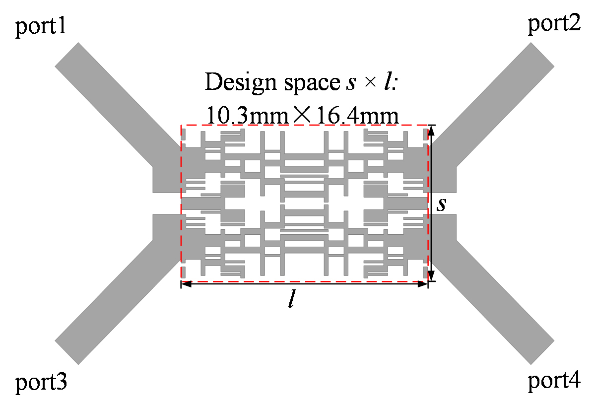
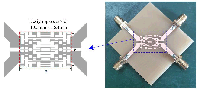
Figure 3: The layout of 20-dB director with 2-bit FTS scheme.
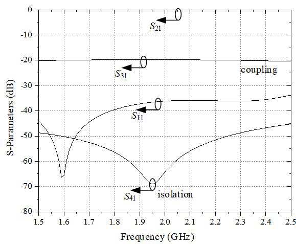
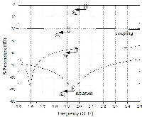
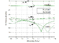
Figure 4: S-parameters of the 20-dB directional coupler with 2-bit FTS.
Figure 4 presents the simulated and measured S-parameters. In the operation band, the simulated minimum return loss is 33 dB, the maximum insertion loss is 0.8 dB, the isolation is greater than 45 dB, and the maximum isolation is 69 dB. The coupling level is 20 dB 0.5 dB in frequency band ranging from 1.5 GHz to 2.5 GHz, which gives a fractional bandwidthof 50%.
Directivity of the 20-dB coupler can be calculated from the S-parameters in Figure 4. The minimum directivity is D = 27.5 dB and the maximum directivity is D = 49 dB in the operation bandwidth. Therefore, the proposed 2-bit FTS can be used in design of wideband high-directivity 20-dB directional coupler without any slot presetting.
B. Design of 10-dB directional coupler
For the 10-dB directional coupler, the design objectives are set with C = 10 dB in eqn (1), with = 0.5 in eqn (2), Q = 70 in eqn (3), R = 40 in eqn (4), andBW = 40% in eqn (5) to challenge high performance. The coupler is desired to operate in band [, ] = [1.6 GHz, 2.4 GHz].
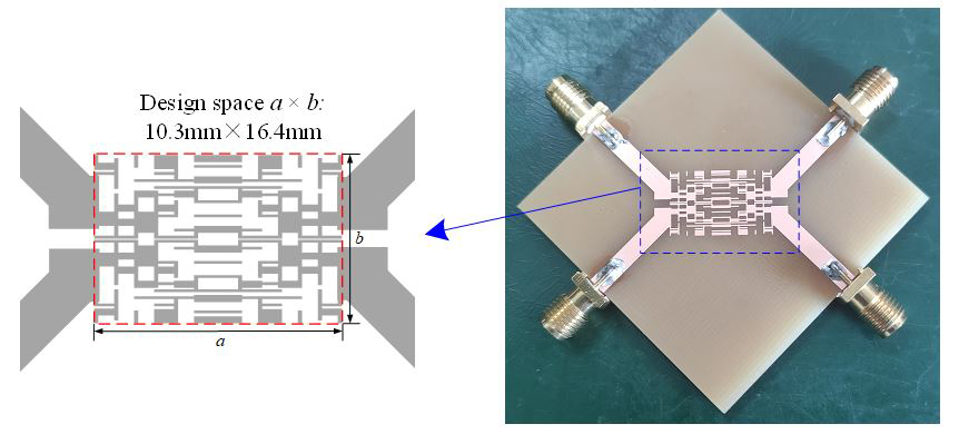
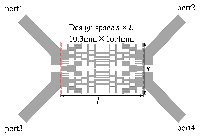
Figure 5: The 10-dB directional coupler designed with 2-bit FTS.
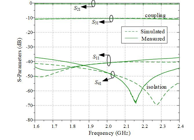
Figure 6: S-parameters of the 10-dB directional coupler with the 2-bit.
After implementing the MOEA/D-GO optimization with the same objectives, optimal layout of the 10-dB directional coupler is obtained and prototype is fabricated, as shown in Figure 5. The optimization searching takes 50 iterations (around 80 hours on the abovementioned computer).
Figure 6 presents the simulated and measured S-parameters. In the operation band, the simulated minimum return loss is 40 dB, the maximum insertion loss is 0.8 dB, the isolation is greater than 41 dB, and the maximum isolation is 69.5 dB. The measured minimum return loss is 37 dB, the isolation is greater than 38 dB, and the maximum isolation is 68 dB.
Directivity of the fabricated coupler is calculated from the measured S-parameters in Figure 6. The minimum directivity is D = 27.5 dB and the maximum directivity is D = 58 dB in an operation bandwidth of 36% (from 1.62 GHz to 2.34 GHz). The phase difference between Port 2 and Port 3 is900.5.
C. Reference formatting
Since the 20-dB directional coupler design with 1-bit FTS in [12] provides the most competitive performance, we may just compare the designed coupler with the 1-bit FTS coupler in [12]. We find that the 2-bit FTS coupler presented in this paper acquires broader bandwidth of 50%, which is 40% provided by 1-bit FTS coupler in [12]. And the maximum directivity is 49 dB, which is slightly higher than that obtained by 1-bit FTS coupler in [12]. But lower minimum directivity is obtained to be 27.5 dB, which is 37 dB acquired by 1-bit FTS coupler in [12]. However, it is still higher than the minimum directivities (around 20 dB) of wideband planar directional couplers designed by using conventional structures and techniques.
Table 1: Comparison between different 10-dB directional couplers
| Designs | f | Bandwidth | D | D | Design area |
| (GHz) | (dB) | (dB) | () | ||
| [4] | 1 | 27.7% | 20 | 28 | 0.20.03 |
| [7] | 2 | 8.7% | 20 | 40 | 0.350.46 |
| [10] | 6.2 | 24% | 15 | 30 | 0.90.29 |
| [12] | 2 | 29% | 28.7 | 44.6 | 0.250.1 |
| 2-bit FTS | 2 | 36% | 27.5 | 58 | 0.250.1 |
simulation results only. |
|||||
As for the 10-dB coupler, comparison with other 10-dB directional couplers reported in literatures are listed in Table 1. The FTS couplers designed with the 2-bit FTS scheme provide broader bandwidth and higher directivity. In addition, they have a compactsize.
IV. CONCLUSION
The 2-bit FTS scheme can be used for automatic design of microstrip directional coupler. With the 2-bit FTS coding, design matrix of size twice that for conventional 1-bit FTS can be acquired, which is very efficient for treating fine or subtle structures in the multi-objective optimization searching. The automatic design of planar directional couplers can complete in days without any apriority about coupler structures, any structure presetting or artificial intervention.
ACKNOWLEDGMENT
This work was funded in part by NationalNatural Science Foundation of China under Grant 61671421, Natural science fund for colleges and universities in Jiangsu Province (Grant no. 20KJB510005), and Scientific Research Foundation for Doctors of Jinling Institute of Technology (Grant no. jit-b-201718).
REFERENCES
[1] M. K. Krage and G. I. Haddad, “Characteristics of coupled microstrip transmission lines-I: Coupled-mode formulation of inhomogeneous lines,” IEEE Trans. Microw. Theory Tech., vol. 18, no. 4, pp. 217-222, Apr. 1970.
[2] C. Liu, T. Yang, K. Huang, and W. Menzel, “Compact capacitive compensated directional coupler using planar artificial transmission lines,” Electron. Lett., vol. 47, no. 24, pp. 1321-1323, Nov.2011.
[3] J. Ha, W. Shin, and Y. Lee, “An inductive-loading method for directivity enhancement of microstrip coupled-line couplers,” IEEE Microwave and Wireless Components Letters., vol. 27, no. 4, pp. 356-358, Apr. 2017.
[4] R. Phromloungsri, M. Chongcheawchamnan, and I. D. Robertson, “Inductively compensated parallel coupled microstrip lines and their applications,” IEEE Trans. Microw. Theory Techn., vol. 54, no. 9, pp. 3571-3582, Sep. 2006.
[5] M. Akhtar M, M. Zakir, and H. Cheema, “Weakly coupled directional coupler with simultaneous wide bandwidth and high directivity,” Microw Opt Technol Lett., vol. 61, pp. 1259-1262, 2019.
[6] D. Jaisson, “Multilayer microstrip directional coupler with discrete coupling,” IEEE Trans. Microw. Theory Techn., vol. 48, no. 9, pp. 1591-1595, Sep. 2000.
[7] A. Pourzadi, A. R. Attari, and M. S. Majedi, “A directivity-enhanced directional coupler using epsilon negative transmission line,” IEEE Trans. Microw. Theory Techn., vol. 60, no. 11, pp. 3395-3402, 2012.
[8] B. S. Yldrm and K. Karayahşi, “Broadband UHF directional coupler with high directivity,” Fifth International Electromagnetic Compatibility Conference (EMC Turkiye), Sep. 2019.
[9] A. Agharasuli, M. K. Mehr, O. Manoochehri, and D. Erricolo, “UWB stripline coupler with low loss and ripple,” Proc. International Conference on Electromagnetics in Advanced Applications (ICEAA), Sep. 2019.
[10] P. Mondal and S. Parui, “Multi-mode resonator based asymmetric broadband 10db directional coupler,” 3rd International Conference on Microwave and Photonics (ICMAP), Feb. 2018.
[11] J. Shi, X. Y. Zhang, K. W. Lau, J. X. Chen, and Q. Xue, “Directional coupler with high directivity using metallic cylinders on microstrip line,” Electron. Lett., vol. 45, no. 8, pp. 415-417, Apr.2009.
[12] L. Wang, G. Wang, and J. Siden, “Design of high-directivity wideband microstrip directional coupler with fragment-type structure,” IEEE Trans. Microw. Theory Tech., vol. 63, no. 12, pp. 3962-3970, Oct. 2015.
[13] W. Zhang and G. Wang, “Design of compact planar lowpass filters by using fragment-type structure with multi-bit scheme,” IEEE Access, vol. 9, pp. 74143-74154, 2021.
BIOGRAPHIES

Yonghui Tao received the Ph.D. degree from University of Science and Technology of China, Hefei, China, in 2014. From 2015 to 2017, she worked at University of Science and Technology of China as a Postdoctoral Research Fellow supported by the Chinese government.
She is currently an instructor with Jinling Institute of Technology. Her research interests involve radio-frequency identification, microwave hyperthermia, metamaterials and its applications in biomedicalengineering.

Wenjuan Zhang received the B.S. degree from Xidian University, Xi’an, China, in 2016. She is currently pursuing the Ph.D. degree in electrical engineering with the University of Science and Technology of China, Hefei, China. Her research interests include microwave/RF circuit theory and design technique, RFID, and sensor design.

Johan Sidén (M’00) received the M.Sc. degree in telecommunication, the Licentiate of Technology degree in electronics, and the Ph.D. degree in electronics from Mid Sweden University, Sundsvall, Sweden, in 2000, 2004, and 2007, respectively.
He is currently an Associate Professor with Mid Sweden University. His current research interests include radio-frequency identification technology, wireless sensor networks, antenna technology, printed passive electronic systems, and optical fiber installationsystems.

Gang Wang (M’98) received the B.S. degree from the University of Science and Technology of China, Hefei, China, in 1988, and the M.S. and Ph.D. degrees in electrical engineering from Xidian University, Xi’an, China, in 1991 and 1996, respectively.
From 1996 to 1998, he was with Xi’an Jiaotong University, as a Postdoctoral Research Fellow, supported by the Chinese Government. From 1998 to 2000, he was an Associate Professor with Xi’an Jiaotong University. In 2001, he was a Visiting Researcher with the Department of ITM, Mid-Sweden University. From 2002 to 2003, he was a Postdoctoral Research Associate with the Department of Electrical and Computer Engineering, University of Florida. From 2003 to 2010, he was with Jiangsu University, China, as a Chair Professor. He is currently a Full Professor with the University of Science and Technology of China. His current research interests include autonomous driving, RFID/sensor technology, and microwave circuit, and antennadesign.
ACES JOURNAL, Vol. 36, No. 12, 1610–1615.
doi: 10.13052/2021.ACES.J.361213
© 2021 River Publishers