Electronically Steerable Parasitic Patches for Dual-Polarization Reconfigurable Antenna Using Varactors
Yajie Mu, Jiaqi Han, Dexiao Xia, Xiangjin Ma, Haixia Liu, and Long Li
Key Laboratory of High-Speed Circuit Design and EMC of Ministry of Education, School of Electronic Engineering, Xidian University, Xi’an 710071, China
hxliu@xidian.edu.cn, lilong@mail.xidian.edu.cn
Submitted On: October 2, 2021; Accepted On: January 28, 2022
Abstract
This paper presents a dual-polarized reconfigurable antenna loading electronically steerable parasitic patches. The proposed dual-polarized antenna is surrounded by four parasitic patches each of which is mounted by two varactor diodes on the ground. By tuning the varactors, continuous two-dimensional beam-steering can be achieved for each of the polarization. A prototype of the proposed antenna is fabricated and measured. Excellent agreement between the simulated and measured results is observed. It is observed that the maximum beam-scanning angles in E-plane and H-plane are greater than 25, which is suitable for 5G base station applications.
Keywords: Dual-polarized antenna, reconfigurable pattern antenna, parasitic patch, varactor.
I. INTRODUCTION
With the rapid development of wireless communication, there are increasing needs for high-speed, low-latency, and large-capacity wireless communications. The widely used dual-polarized antenna can effectively improve the communication capacity through polarization diversity [1, 2, 3, 4, 5, 6, 7, 8]. Additionally, the pattern reconfigurable antennas are capable of steering the beam pointing, reducing noise interference and increasingsignal coverage [9, 10]. Therefore, a dual-polarized pattern reconfigurable antenna can improve channel capacity and mitigate multi-path propagation fading.
Essentially, the pattern reconfigurable antennas can be achieved by adding active components (e.g., PIN diode, varactor, MEMS, etc.) on parasitic patches indirectly [9, 10, 11, 12] or radiator directly [13, 14, 15]. The directly loaded manner affects the surface current flow path, while the indirectly loaded manner tunes parasitic patches to realize pattern reconfigurability. The active tuned parasitic patches are more flexible and transplantable compared to directly loaded manner. The main reason is that the parasitic patches do not change the structure of the driven antenna. The parasitic patches in the pattern reconfigurable antenna have various structures, such as rectangle, circle, and octagon, etc. Among them, the rectangular parasitic structure is the most commonly used. In the papers [16] and [20], the rectangular parasitic patches are adopted to achieve pattern reconfigurable antenna. In the paper [9], the parasitic patches are octagon structures that can obtain four pattern modes by adjusting the connection state of the parasitic patches and the ground. Moreover, there are very few dual-polarized pattern reconfigurable antennas. In the paper [9], a dual-polarized pattern reconfigurable Yagi patch antenna was proposed, which can achieve four-mode patterns in both polarizations. However, it uses eight PIN diodes to implement two deflection modes and only one can achieve one-dimensional beam-steering. In the papers [13] and [21], the directly loaded manner is used to tune the current of antenna radiators which can achieve pattern reconfigurableantenna.
In addition, there are many ways to realize a reconfigurable antenna pattern [18, 19, 20, 21, 22, 23, 24]. An artificial ground structure was reconfigured with PIN diodes inserted on the bottom ground to adjust the pattern of the antenna [18]. A broadside radiation pattern and a conical pattern were obtained when it alternatively operates in the TM10 mode and TM02 mode of the rectangular patch [19]. The optically transparent and compact dual-band, polarization-angle-independent metasurfaces have reconfigurable patterns for ambient energy harvesting and wireless power transfer [25, 26].
In this paper, electronically tuned parasitic patches using varactors are assigned in the surrounding area of a driven dual-polarized antenna to implement pattern reconfigurability. This work aims to design a two-dimensional dual-polarized pattern reconfigurable antenna. We propose a single antenna model that can explain the pattern reconfigurable principle of the capacitance-loaded parasitic patches. An antenna prototype is fabricated and measured. Continuously two-dimensional dual-polarized beam pointing adjustment is achieved.
This paper is organized as follows. Section II introduces the design principle of pattern reconfigurable antenna and the steps to achieve the dual-polarization pattern reconfigurable antenna. The dual-polarization reconfigurable antenna is introduced in great detail in Section III. Section IV describes the pattern reconfigurable results. The measured results of the dual-polarization pattern reconfigurable antenna are given in Section V. The conclusion is given in Section VI.
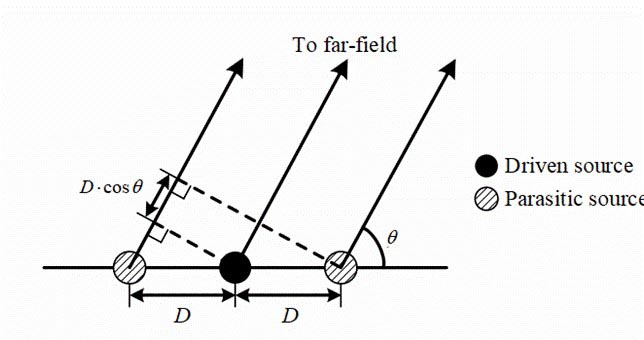
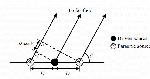
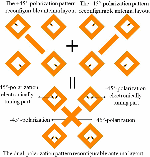
Figure 1: Qualitative analysis for one driven source and two varactor-loaded parasitic sources.
II. DESIGN PRINCIPLE
Fundamentally, the pattern reconfigurable principle of the proposed antenna is to change the surface current phase of the parasitic patches by loading unequal capacitance. The induced current with unequal phases would reradiate to form the desired patterns. Although numerous studies have discussed the parasitic patches tuned antennas [27], the mechanism by loading lumped components on parasitic patches has not beenestablished.
In this paper, we qualitatively analyze the antenna which is tuned by capacitance-loaded parasitic patches. The proposed antenna for each polarization can be regarded as the three-point source. The central source is the driven source and the sibling two are parasitic sources, as shown in Figure 1. The driven source is referred to as the phase center point. Thereby, as the theory of point sources array [28], the far-field pattern can be expressed as
| (1) |
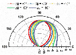
where and are the driven and parasitic source amplitude at far-field, k Dcos is the phase difference of parasitic source referring to the driven source, and is the tunable phase. Based on these assumptions, patterns of the three-point sources are calculated and shown in Figure 2. Distance between the driven source and the parasitic source is D = 0.32 and = 0.6. It can be seen that the main beam pattern deflects when the tunable phase changes. This indicates that a pattern reconfigurable antenna can be achieved when we introduce unbalanced capacitance which results in an unbalanced phase on either side of parasitic arms.
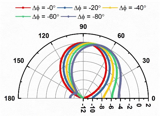
Figure 2: Normalized patterns for different on the parasitic source.
In this paper, electronically tuned parasitic patches using varactors are assigned in the surrounding area of a driven dual-polarization antenna to implement pattern reconfigurability. The unbalanced phase for achieving pattern reconfigurability on the parasitic patches is achieved by the unbalanced capacitance. The unbalanced capacitance is represented by C which is the capacitance difference of each pair of varactors.
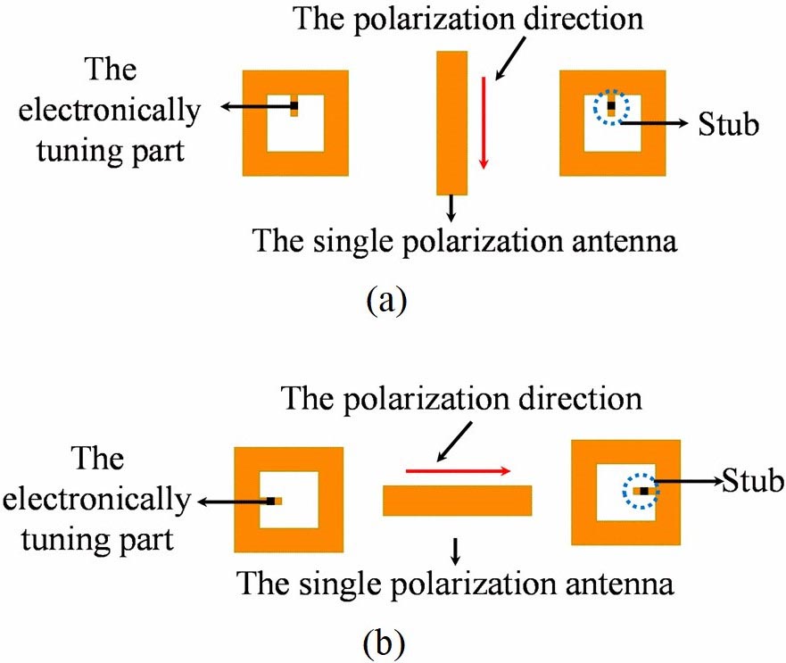
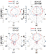
Figure 3: (a) The reconfigurable pattern of the single-polarization antenna in H-plane. (a) The reconfigurable pattern of the single-polarization antenna in E-plane.
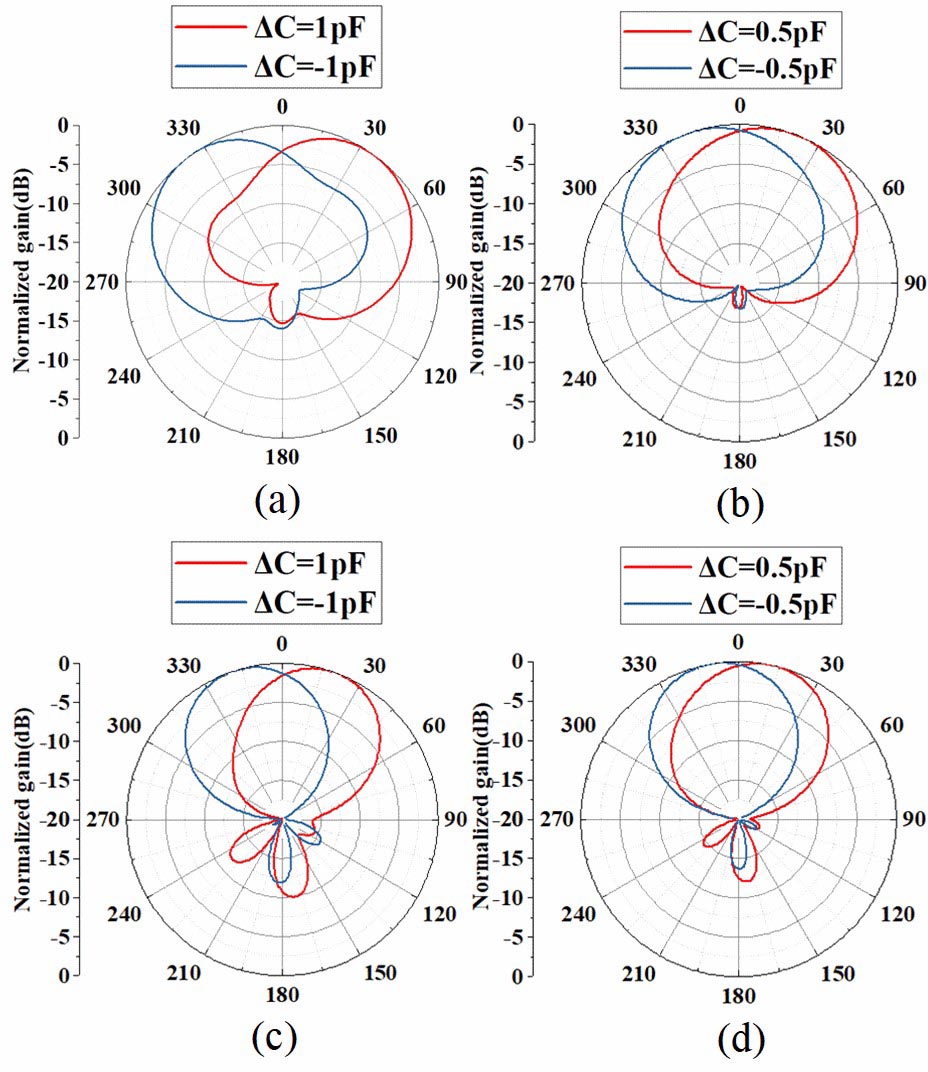
Figure 4: (a) and (b) The reconfigurable patterns of the single-polarization antenna with different capacitance values in the H-plane. (c) and (d) The reconfigurable pattern of the single-polarization antenna with different capacitance values in E-plane.
The dual-polarization pattern reconfigurable antenna can be decomposed into two single-polarization patterns reconfigurable antenna. Due to the two polarizations being symmetrical, we only need to analyze how one of the single polarization antennas realizes the reconfigurable pattern. The single polarization antenna can achieve the reconfigurable pattern when parasitic patches are assigned in H-plane and E-plane, respectively, as shown in Figure 4(a) and (b), where the electronically tuned arms must be parallel to the antenna polarization direction to control the antenna pattern. In Figure 4(a), the antenna can achieve the reconfigurable pattern with different C in H-plane, as shown in Figure 4(a) and (b). When C = 1 pF and C = 1 pF, the beam deflection angles are 36 and 37 in H-plane, respectively. Similarly, when C = 0.5 pF and C = 0.5 pF, the beam deflection angles are 21 and 21 in H-plane, respectively. Therefore, the single polarization antenna can achieve the reconfigurable pattern in H-plane when the capacitance differences are introduced on parasitic patches in H-plane. In addition, the antenna can achieve the reconfigurable pattern with different C in E-plane, as shown in Figure 4(b). In Figure 4(c), when C =1 pF and C = 1 pF, the beam deflection angles are 20 and 18 in E-plane, respectively. Similarly, in Figure 4(d), when C = 0.5 pF and C = 0.5 pF, the beam deflection angles are 13 and 11 in E-plane, respectively. Therefore, the single polarization antenna can achieve the reconfigurable pattern in E-plane when the capacitance differences are introduced on parasitic patches in E-plane. According to the above analysis, the single polarization antenna can realize the reconfigurable pattern in two-dimensional directions by loading two electrically tuned parasitic patches in the E-plane and H-plane, respectively.
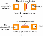
For E-plane or H-plane reconfigurable pattern, two parasitic patches are needed at least, which are placed on scanning plane. Hence, four parasitic patches are arranged to achieve the two-dimensional reconfigurable pattern in a single polarization antenna. Therefore, the two-dimensional dual-polarization pattern reconfigurable antenna is made of two orthogonal single-polarized antennas that have two-dimensional pattern reconfigurability, as shown in Figure 5. For a 45 dual-polarization antenna, the E-plane of +45-polarization is the H-plane of 45-polarization. Therefore, the E-plane parasitic patches of +45 polarization and the H-plane parasitic patches of the 45 polarization are in the same area where the +45 and 45 polarization can share a parasitic patch. These shared parasitic patches have the electronically tuning parts along each polarization direction. Therefore, the dual-polarization antenna has pattern reconfigurability in two-dimensional directions by shared parasitic patches, as shown in Figure 5.
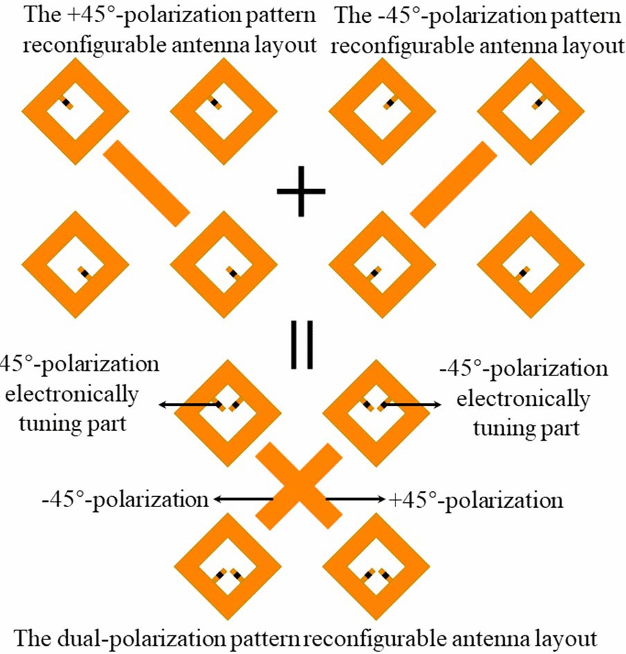
Figure 5: The single polarization pattern reconfigurable antenna layout and the dual-polarization pattern reconfigurable antenna layout with two-dimensional beam-steering.
III. ANTENNA DESIGN
As mentioned before, the indirectly loaded pattern reconfigurable antennas are composed of a driven antenna and parasitic patches. And the two-dimensional beam-steering scheme of dual-polarized antennas is also analyzed in the previous section. In this section, the specific design scheme of the dual-polarization antenna with a two-dimensional reconfigurable pattern ispresented.
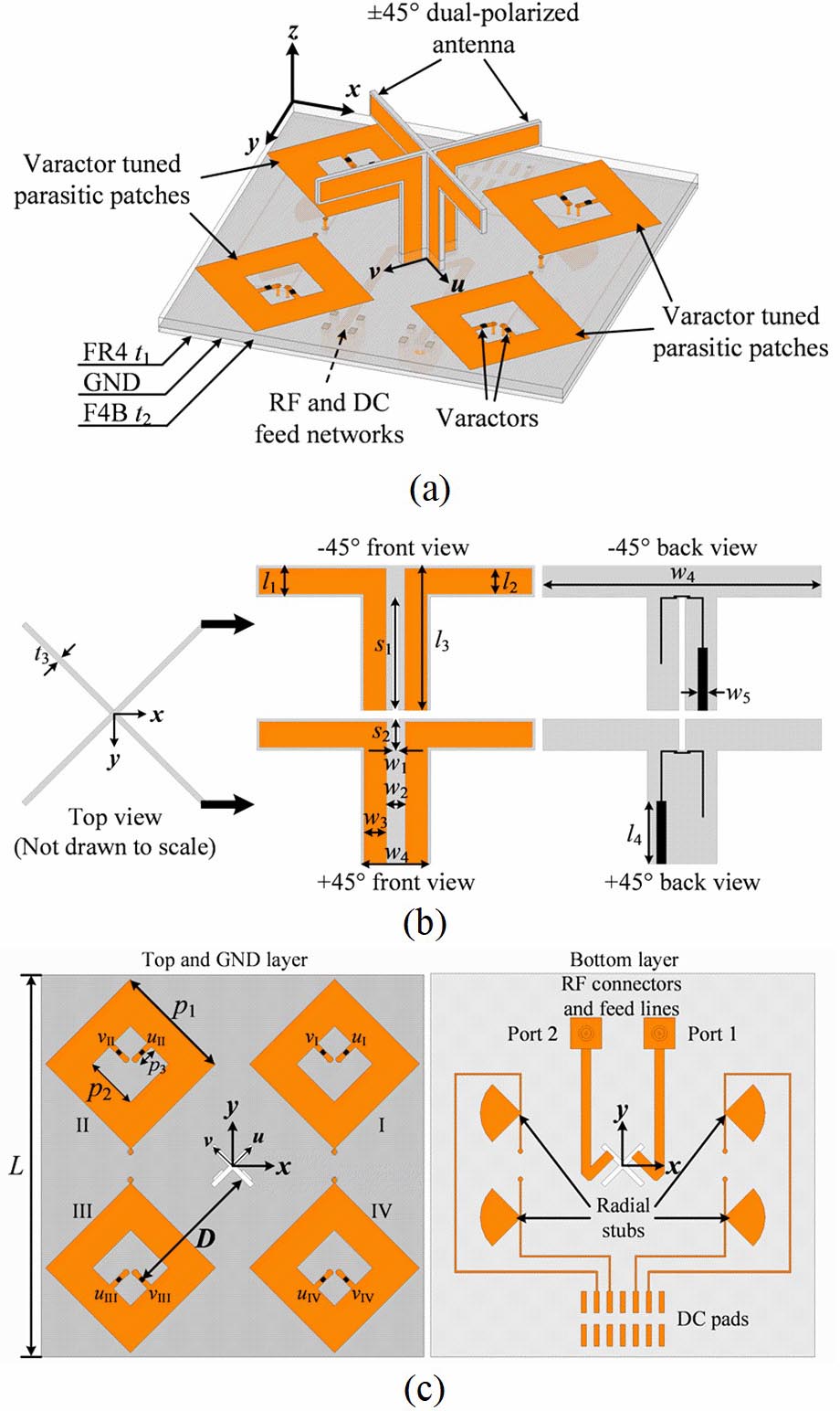
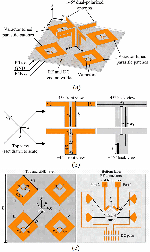
Figure 6: Topology of the proposed antenna. (a) Perspective view, (b) dual-polarized antenna, and (c) varactor-tuned parasitic patches with DC bias lines (the four patches are labeled as I, II, III, and IV anticlockwise).
The geometrical topology of the proposed antenna is shown in Figure 6(a). It can be seen that it has a 45 dual-polarized dipole antenna and four parasitic patches, which are tuned by eight varactors. The orthogonal u- and v-directions are defined to represent the = +45 and = 45 polarization directions, respectively.
Detailed geometrical structure of the dual-polarized antenna located at the center is shown in Figure 6(b). The printed dipole antennas have compact configurations for dual-polarized operations. The structure of the two dipole antennas is almost the same except for substrate shape and feed lines. The substrate for the printed dipole antennas is FR4 (= 4.4, tan = 0.02). For each polarization, the dipole is integrated with a balun which connects to a 50- SMA connector [26].
The parasitic patches, reflective ground plane, and direct circuit (DC) bias lines are shown in Figure 4(c). The four capacitance-loaded parasitic patches are etched on an FR4 substrate, which is assigned along with two polarizations. It can be seen that patches I and III lie in the u-plane, while patches II and IV lie in the v-plane. To realize a two-dimensional dual-polarized pattern reconfigurable, two arms along u- and v-directions, which are mounted by varactors, are designed on each parasitic patch.
The model of the varactor used in this design is Skyworks SMV1430 whose junction capacitance ranges from 0.31 to 1.24 pF as reverse voltage changes from 30 to 0 V. Package series inductance is 0.45 nH. The varactors are soldered in the 0.5-mm gap of parasitic patches arms. A F4B substrate ( = 2.5; tan = 0.005) separates the ground layer and feed networks. The radio frequency (RF) connectors and DC feed lines are integrated into the bottom layer as shown in Figure 6(c). Four radial stubs are designed to choke RF signals.
For simplicity, we label the varactor by direction combined with the patch index. For example, the pattern of the dipole in the u-plane (+45 polarization) can be steered to scan in u-plane by using uand u varactors, while as u and u varactors are used, the pattern can scan in v-plane. In other words, there are four tuned arms to steer the radiation pattern of each polarization. A pair of varactors steer the pattern scanning in E-plane and the other pair of varactors steer the pattern scanning in H-plane. All the structural parameters are listed in Table 1. Central operating frequency of the proposed antenna is 3.4 GHz.
Table 1: Parameter values ( at 3.4 GHz)
| Parameters | Values | Parameters | Values |
|---|---|---|---|
| t | 1 mm | w | 3.5 mm |
| t | 2 mm | w | 44 mm |
| t | 1 mm | s | 18 mm |
| l | 5 mm | s | 5 mm |
| l | 4 mm | L | 75 mm |
| l | 23 mm | D | 28.3 mm |
| l | 10 mm | p | 23.5 mm |
| w | 1 mm | p | 10.6 mm |
| w | 3 mm | p | 4.3 mm |
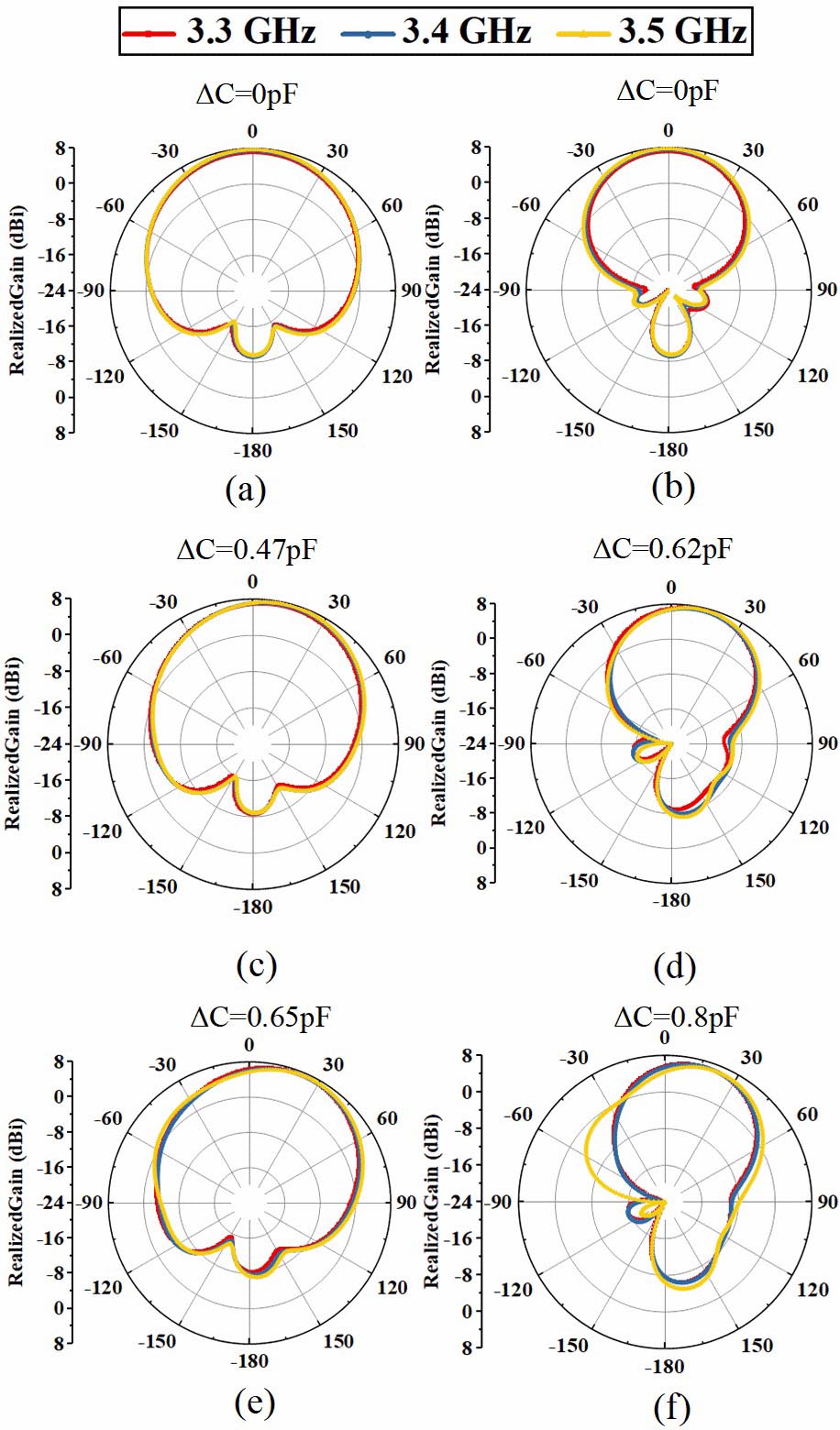
Figure 7: Simulated gain patterns deflection in E-plane and H-plane at different frequencies when C varies. (a), (c), and (e) Patterns in E-plane. (b), (d), and (f) Patterns in H-plane.
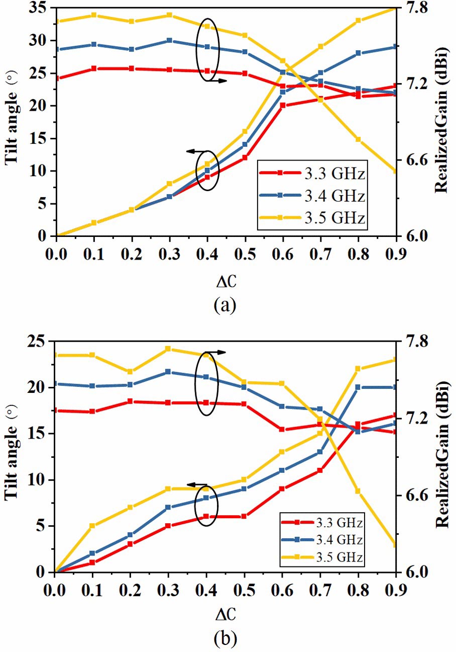
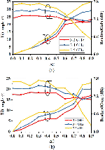
Figure 8: Tilt angle and peak gain in (a) E-plane and (b) H-plane versus C at different frequencies.
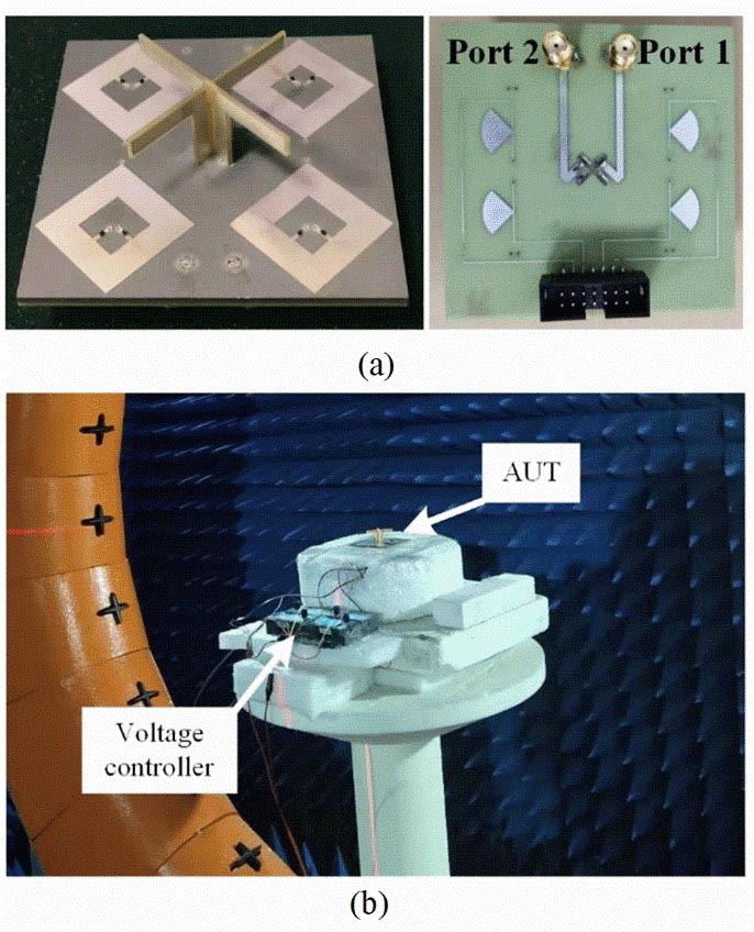
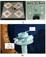
Figure 9: Fabricated two-dimensional dual-polarized pattern reconfigurable antenna. (a) Fabricated antenna prototype. (b) Measurement scene.
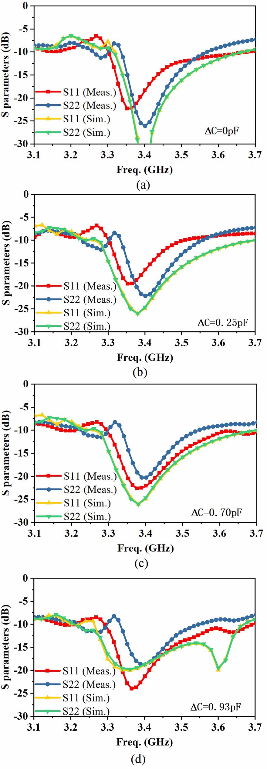
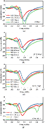
Figure 10: Simulated and measured reflection coefficients for different C. (a) C = 0 pF. (a) C = 0.25 pF. (a) C = 0.70 pF. (a) C = 0.93 pF.
IV. PATTERN RECONFIGURABLE RESULT
Ansys HFSS 15.0 is applied to simulate the proposed antenna. The varactor is simulated by a capacitor in series with an inductor using lumped RLC boundary conditions. The varactor is characterized by the varying capacitance value of the capacitor. Here, the capacitance difference of each pair of varactors is defined as C for simplicity. As shown in Figure 7, the simulated gain patterns, which take into the mismatch loss account, with different deflection angles are presented for different C. Both E-plane and H-plane simulated results are plotted. It can be seen that the tilt patterns show similarly reconfigurable results within the working frequency band. In this case, only Port 1 is excited and Port 2 has similar results. Varactor pair of u and u controls the pattern tilt in E-plane, while u and u control the pattern tilt in H-plane, which can be controlled independently. Pattern tilt angles at 3.5 GHz are 0, 16, and 27 in E-plane, while in H-plane, they are 0, 13, and 22 for different C, as shown in Figure 7. The peak gains are 7.69, 7.58, and 7.21 dBi in E-plane, while in H-plane 7.69, 7.37, and 6.63 dBi, respectively. It should be noted that for the same C, the pattern deflection angles are not identical in E-plane and H-plane.
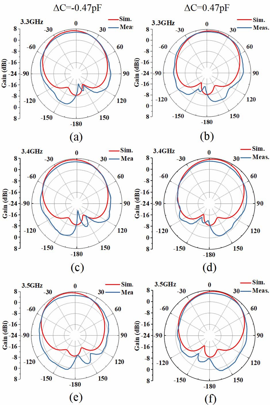
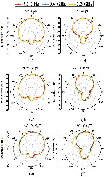
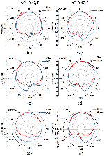
Figure 11: Simulated and measured E-plane gain patterns for C = 0.47 pF and C = 0.47 pF at different frequencies with Port 1 excited. (a), (c), and (e) Patterns at 3.3, 3.4, and 3.5 GHz for C = 0.47 pF. (b), (d), and (f) Patterns at 3.3, 3.4, and 3.5 GHz for C = 0.47 pF.
For the detailed variation of the pattern tilt angle versus C, we simulated the proposed antenna under different C when Port 1 is excited, as shown in Figure 8. From the results, it suggests that pattern deflection angle increases with C. Meanwhile, peak gain decreases due to scanning loss and mismatch loss. At 3.5 GHz, the proposed antenna possesses a maximum deflection angle of 35 and its peak gain drops to 6.5 dBi accordingly in E-plane, as shown in Figure 8(a). Similar results can be obtained for H-plane deflection that the proposed antenna possesses a maximum deflection angle of 28 and its peak gain drops to 6.21 dBi accordingly at 3.5 GHz, as shown in Figure 8(b). Similar results can be obtained for Port 2 which is a +45 polarization antenna. The different deflection angles of the E-plane and H-plane patterns are caused by the different coupling of the antenna to the E-plane and H-plane. Through the above simulation results, it can be analyzed to get that we proposed antenna possess two-dimensional dual-polarization patternreconfigurability.
V. MEASUREMENT RESULTS
The fabricated prototype of the proposed antenna is shown in Figure 9(a). Simulated and measured reflection coefficients for different C are shown in Figure 10. Note that Port 1 C represents the capacitance difference of u and u, while Port 2 C represents the capacitance difference of v and v. It can be observed that the measured results agree with the simulated ones as C changed. However, the measured reflection coefficients of the two ports are not overlapped exactly. A possible explanation for this might be the variation of actual capacitance of the varactor and designed data obtained from the manufacturer’s datasheet.
The antenna is measured in a multi-probe anechoic chamber, as shown in Figure 9(b). Four voltage controllers that can continuously generate 030 V voltage are applied to bias the varactors for two-dimensional beam-steering. The measured and simulated E-plane patterns within the working frequency band as Port 1 excited are shown in Figure 11. For simplicity, only the deflection pattern under a certain capacitance difference on the E-plane is given. We tuned the voltage controller to set C of u and u as 0.47 and 0.47 pF. From the comparisons, we can clearly see that measured patterns are deflected to the intended directions for each frequency. At 3.3 GHz, peak gains, which are 5.80 and 5.92 dBi, occur at = 16 and = 18 when C is equal to 0.47 and 0.47 pF, respectively. At 3.4 GHz, peak gains, which are 5.89 and 5.81 dBi, occur at = 14 and = 16 when C is equal to 0.47 and 0.47 pF, respectively. At 3.5 GHz, peak gains, which are 5.74 and 5.96 dBi, occur at = 24 and = 28 when C is equal to 0.47 and 0.47 pF, respectively. There exists a discrepancy of beam pointing and gain-loss between simulated and measured results. They are caused by fabrication errors and measurement tolerance. The back lobes of the measured patterns are larger than simulated ones. This may be due to the support platform. The measured efficiency of the antenna is above 50%, a little lower than that of the simulated one. Nevertheless, the measured results validate the good performance of the proposed antenna. In addition, the measured cross-polarization discriminations are higher than 12.5 dB, which satisfies the requirement of communication.
Table 2: Comparison of this work with some existing works
| Ref. | DP | PR | PR dim. | BW (%) |
| [3] | Yes | No | NA | 44.5% |
| [9] | Yes | Yes | 1 | 5.6% |
| [14] | No | Yes | 1 | 58% |
| [15] | No | Yes | 1 | 0.6% |
| [24] | No | Yes | 1 | 20.8% |
| This work | Yes | Yes | 2 | 5.9% |
Note: DP: Dual polarization; PR: polarization reconfigurability; PR dim.: PR dimension; BW: bandwidth.
In Table 2, the proposed antenna is compared with some existing works. It can be seen that only [9] and the work of this paper are about the reconfigurable pattern of dual-polarization antennas, and the bandwidth of this paper is wider. In addition, only the proposed antenna has a two-dimensional dual-polarization pattern reconfigurable ability. And the antenna can achieve continuous steering.
VI. CONCLUSION
A dual-polarized pattern reconfigurable antenna has been proposed and fabricated in this paper. This antenna is capable of continuously steering patterns in E- and H-planes by using varactors tuned parasitic patches. The proposed parasitic patches topology can be transplanted to other frequency bands. Two-dimensional pattern deflection exceeds 50. Measured reflection coefficients are less than 10 dB from 3.3 to 3.5 GHz for two ports when continuously steering the beam pointing. Validation of the prototyped antenna indicates that the proposed varactor-tuned parasitic patches can effectively direct the pattern of the driven antenna, which is coincident with the qualitative analysis.
ACKNOWLEDGEMENT
The authors acknowledge the National Key Research and Development Program of China under Grant 2021YFA1401001, the National Natural Science Foundation of China under Grant 62001342, the Key Research and Development Program of Shaanxi under Grant 2021TD-07, and the Outstanding Youth Science Foundation of Shaanxi Province under Grant 2019JC-15.
REFERENCES
[1] S. Kozono, T. Tsuruhara, and M. Sakamoto, “Base station polarization diversity reception for mobile radio,” IEEE Transactions. Vehicle Technology, vol. 33, no. 4, pp. 301-306, 1984.
[2] Q. Chu, D. Wen, and Y. Luo, “A broadband dual-polarized antenna with Y-shaped feeding lines,” IEEE Transactions on Antennas and Propagation, vol. 63, no. 2, pp. 483-490, 2015.
[3] Y. Liu, H. Yi, F. Wang, and S. Gong, “A novel miniaturized broadband dual-polarized dipole antenna for base station,” IEEE Antennas and Wireless Propagation Letters, vol. 12, pp. 1335-1338, 2013.
[4] Z. Bao, Z. Nie and X. Zong, “A novel broadband dual-polarization antenna utilizing strong mutual coupling,” IEEE Transactions on Antennas and Propagation, vol. 62, no. 1, pp. 450-454,2014.
[5] Q. Zhang and Y. Gao, “A compact broadband dual-polarized antenna array for base stations,” IEEE Antennas and Wireless Propagation Letters, vol. 17, no. 6, pp. 1073-1076, 2018.
[6] W. Chen et al., “A low-profile broadband dual-polarized base station antenna using folded dipole radiation element,” IEEE Access, vol. 7, pp. 67679-67685, 2019.
[7] Y. -L. Chen, Y. -Z. Sui, Z. -Q. Yang, X. -Y. Qu, and W. -H. Zong, “A broadband dual-polarized antenna for 2G/3G/4G/5G base station applications,” Applied Computational Electromagnetics Society Journal, vol. 36, no. 9, pp. 1202-1208, 2021.
[8] J. Yin, H. Sun, and L. Zhang, “A wideband wide-beam dual polarized dipole antenna and its application in wideband wide-angle scanning array,” Applied Computational Electromagnetics Society Journal, vol. 35, no. 6, pp. 692-699, 2020.
[9] W. Deng, X. Yang, C. Shen, J. Zhao and B. Wang, “A dual-polarized pattern reconfigurable Yagi patch antenna for microbase stations,” IEEE Transactions on Antennas and Propagation, vol. 65, no. 10, pp. 5095-5102, 2017.
[10] M. A. Hossain, I. Bahceci and B. A. Cetiner, “Parasitic layer-based radiation pattern reconfigurable antenna for 5G communications,” IEEE Transactions on Antennas and Propagation, vol. 65, no. 2, pp. 6444-6452, 2017.
[11] L. Marantis, D. Rongas, A. Paraskevopoulos, C. Oikonomopoulos-Zachos and A. Kanatas, “Pattern reconfigurable ESPAR antenna for vehicle-to-vehicle communications,” IET Microwaves, Antennas and Propagation, vol. 12, no. 3, pp. 280-286, 2018.
[12] S. Raman, N. Timmons and J. Morrison, “Gain enhanced pattern reconfigurable planar yagi-uda antenna on coplanar structure,” Electronics Letters, vol 49, no. 25, pp. 1593 -1595, 2013.
[13] S. Shi and W. Ding, “Radiation pattern reconfigurable microstrip antenna for WiMAX application,” Electronics Letters, vol. 51, no. 9, pp. 662-664, 2015.
[14] S. Ahdi Rezaeieh and A. M. Abbosh, “Pattern-reconfigurable magnetoelectric antenna utilizing asymmetrical dipole arms,” IEEE Antennas and Wireless Propagation Letters, vol. 18, no. 4, pp. 688-692, 2019.
[15] Z. Ding, R. Jin, J. Geng, W. Zhu and X. Liang, “Varactor loaded pattern reconfigurable patch antenna with shorting pins,” IEEE Transactions on Antennas and Propagation, vol. 67, no. 10, pp. 6267-6277, 2019.
[16] S. Xiao, C. Zheng, M. Li, J. Xiong and B. Wang, “Varactor-loaded pattern reconfigurable array for wide-angle scanning with low gain fluctuation,” IEEE Transactions on Antennas and Propagation, vol. 63, no. 5, pp. 2364-2369,2015.
[17] F. Farzami, S. Khaledian, B. Smida and D. Erricolo, “Pattern-reconfigurable printed dipole antenna using loaded parasitic patches,” IEEE Antennas and Wireless Propagation Letters, vol. 16, pp. 1151-1154, 2017.
[18] Y.-F. Cheng, X. Ding, W. Shao, and C. Liao, “A novel beam-steerable antenna using HIS-SWG reconfigurable artificial ground structure,” Applied Computational Electromagnetics Society Journal, vol. 34, no. 1, pp. 107-114, 2019.
[19] H.-Y. Huang, B.-Z. W. Wang, X. Ding, and W. Shao, “A pattern reconfigurable antenna based on TM10 and TM02 modes of rectangular patch,” Applied Computational Electromagnetics Society, vol. 28, no. 8, pp. 693-699, 2013.
[20] W. Li, L. Bao, and Y. Li, “A novel frequency and radiation pattern reconfigurable antenna for portable device applications,” Applied Computational Electromagnetics Society Journal, vol. 30, no. 12, pp. 1276-1285, 2015.
[21] M. Saravanan and M. J. S. Rangachar, “Design of Pin loaded reconfigurable patch antenna for wireless communications,” Applied Computational Electromagnetics Society Journal, vol. 34, no. 10, pp. 1535-1541, 2019.
[22] M. A. Wazie, A.-F. A. Sheta, and W. A. Malik, “RF MEMS switches enabled H-shaped beam reconfigurable antenna,” Applied Computational Electromagnetics Society Journal, vol. 34, no. 9, pp. 1312-1318. 2019.
[23] Y. Zhang, D. Sun, T. Dong, and J. Yin, “Design of reconfigurable patch antenna in frequency, pattern, and switchable polarization,” Applied Computational Electromagnetics Society Journal, vol. 35, no. 9, pp. 1037-1046, 2020.
[24] R. Li, H. Yang, B. Liu, Y. Qin and Y. Cui, “Theory and realization of a pattern-reconfigurable antenna based on two dipoles,” IEEE Antennas and Wireless Propagation Letters, vol. 17, no. 9, pp. 1291-1295, 2018.
[25] L. Li, X. Zhang, C. Song, W. Zhang, T. Jia and Y. Huang, “Compact dual-band, wide-angle, polarization-angle-independent rectifying metasurface for ambient energy harvesting and wireless power transfer,” IEEE Transactions on Microwave Theory and Techniques, vol. 69, no. 3, pp. 1518-1528, March 2021.
[26] L. Li, P. Zhang, F. Cheng, M. Chang, and T. J. Cui, “An optically transparent near-field focusing metasurface,” IEEE Transactions on Microwave Theory and Techniques, vol. 69, no. 4, pp. 2015-2027, April 2021.
[27] Y. Gou, S. Yang, J. Li and Z. Nie, “A compact dual-polarized printed dipole antenna with high isolation for wideband base station applications,” IEEE Transactions on Antennas and Propagation, vol. 62, no. 8, pp. 4392-4395, 2014.
[28] J. D. Kraus and R. J. Marhefkas, “Antennas: For all applications” (New York, NY, USA: McGraw-Hill, 2002, 3rd ed.)
BIOGRAPHIES

Yajie Mu was born in Gansu, China, in 1997. She received the B.E. and M.S. degrees in electromagnetic fields and microwave technology from Xidian University, Xi’an, China, in 2018 and 2021, respectively.
Her current research interests include antenna decoupling, pattern reconfigurable antenna, and large angle scanning array.

Jiaqi Han was born in Henan, China, in 1991. He received the B.E. degree in electronic and information engineering from Henan Normal University, Xinxiang, China, in 2014, and the Ph.D. degree in electromagnetic fields and microwave technology from Xidian University, Xi’an, China, in 2019.
He is currently a Postdoctoral Fellow with the School of Electronic Engineering, Xidian University. His research interests include the design of programmable metasurfaces and their applications on wireless power transfer and computational imaging.

Dexiao Xia was born in Jiangxi, China, in 1998. He received the B.E. degree in electronic and information engineering in 2019. He is currently working toward the Ph.D. degree in electromagnetic fields and microwave technology with Xidian University, Xi’an, China, since 2021.
His current research interests include pattern reconfigurable antenna, metasurface antenna decoupling, and array antenna optimization.

Xiangjin Ma was born in Anhui, China, in 1998. He received the B.E. degree in communication engineering from the Nanchang Institute of Technology, Nanchang, China, in 2019. He is currently working toward the Ph.D. degree in electromagnetic field and microwave technology with Xidian University, Xi’an, China.
His current research interests include analysis and application of programmable metasurfaces, design of high-performance programmable metasurfaces, and microwave holographic imaging.

Haixia Liu Haixia Liu received the B.S. and M.S. degrees in test and measurement technique and instrumentation and the Ph.D. degree in electromagnetic fields and microwave technology from Xidian University, Xi’an, China, in 1998, 2001, and 2014, respectively.
She studied at Shizuoka University, Shizuoka, Japan, as a cooperative graduate in 2001. Since 2002, she has been working with Xidian University. His research interests include circuit analysis, frequency measurement and control, wireless power transfer, antennas, and electromagnetic compatibility.

Long Li Long Li received the B.E. and Ph.D. degrees in electromagnetic fields and microwave technology from Xidian University, Xi’an, China, in 1998 and 2005, respectively.
He was a Senior Research Associate with the Wireless Communications Research Center, City University of Hong Kong, Hong Kong, in 2006. He received the Japan Society for Promotion of Science (JSPS) Postdoctoral Fellowship and visited Tohoku University, Sendai, Japan, as a JSPS Fellow from 2006 to 2008. He was a Senior Visiting Scholar with the Pennsylvania State University, State College, PA, USA, in 2014. He is currently a Professor with the School of Electronic Engineering, Xidian University. He is the Director of Key Laboratory of High-Speed Circuit Design and EMC, Ministry of Education, China, and the Dean of Hai-Tang No.9 Academy of Xidian University. His research interests include metamaterials/metasurfaces, antennas and microwave devices, field-circuit collaborative design and EMC, wireless power transfer and harvesting technology, and OAM vortex waves. He has authored or coauthored more than 120 papers in journals and held more than 20 patents.
Dr. Li received Nomination Award of National Excellent Doctoral Dissertation of China in 2007. He won the Best Paper Award in the International Symposium on Antennas and Propagation in 2008. He received the Program for New Century Excellent Talents in University of the Ministry of Education of China in 2010. He won the First Prize of Awards for Scientific Research Results offered by Shaanxi Provincial Department of Education, China, in 2013. He received the IEEE APS Raj Mittra Travel Grant Senior Researcher Award in 2015. He received Shaanxi Youth Science and Technology Award in 2016, and Distinguished Young Scholars Foundation of Shaanxi Province of China, in 2019. He was awarded a Chang-Jiang Distinguished Scholar by the Ministry of Education, China, in 2021. He is the Vice-President of MTT-Chapter in IEEE Xi’an Section. He is a TPC Co-Chair of APCAP2017 and a General Co-Chair of AWPT2019. He serves as an Associate Editor for ACES Journal and Guest Editor for IEEE J-ERM Special Issue.
ACES JOURNAL, Vol. 37, No. 1, 58–67.
doi: 10.13052/2022.ACES.J.370107
© 2021 River Publishers