Multi-Mode Excitation by Interleaved EBG Structure for Suppression of Power/Ground Noise in Multi-Layer PCBs
Ding-Bing Lin, Yen-Hao Chen, and Min-Hung Hsieh
1Department of Electronic and Computer Engineering
National Taiwan University of Science and Technology, Taipei, Taiwan
dblin@mail.ntust.edu.tw, chen.ian@inventec.com
2Signal Integrity Engineering Department
Inventec Corporation, Taoyuan, Taiwan
hsieh.tony@inventec.com
Submitted On: November 5, 2021; Accepted On: May 18, 2022
Abstract
Signal line transition with layer transition via is inevitable in multi-layer PCB. The return current can generate voltage noise between the cavities due to the discontinuity of the return current path. Other layer transition vias passing through the cavity can pick up the voltage noise and result in problems of signal integrity. In this paper, an electromagnetic bandgap (EBG) structure is proposed for suppression of the broadband cavity noise. The impedance discontinuity between layers of interleaved EBG cell enhances the efficiency of noise suppression, and the slots embedded in the EBG cell excite multi-mode resonances for extending the bandwidth of noise suppression. The dispersion diagram is utilized to preliminarily analyze the characteristic of the proposed EBG cell, and a 55 cells EBG board is further analyzed for characterizing the efficiency of noise suppression. Both simulation and measurement results prove the proposed structure can effectively suppress the cavity noise under 35 dB over the frequency range from 0.56 GHz to the highest measurement frequency, 20 GHz.
Index Terms: Electromagnetic bandgap, microwave filter, power/ground noise, signal integrity.
I. INTRODUCTION
With increasing data rate of high-speed digital signal, the nonideal return current path can result in severe power integrity as well as signal integrity problems. The return current with low impedance path is required for the layer transition via passing through multiple layers, as the return current flows through the impedance of the cavity made up of two planes can create a voltage between the planes [1]. The created voltage can propagate in the cavity and should be minimized and suppressed because other layer transition vias passing through the cavity can pick up this voltage noise. To provide a low impedance path for the return current of the layer transition via is an effective approach to suppress the cavity noise and can be achieved by placing decoupling capacitors between power and ground planes [2]. However, the effective inductance (ESL) of the capacitor component limits the bandwidth of the low impedance path of return current. For suppressing the propagation of cavity noise over the effective frequencies limited by the decoupling capacitor, a lot of electromagnetic bandgap(EBG) structures have been proposed to isolate the cavity noise for the GHz application [3–5]. Due to the demand for high density design, an EBG structure with double stacked patches has been proposed for achieving compact size and broadband isolation [6]. That structure is designed with the mushroom-like EBG structure so that it can be practically integrated into existing PCB designs without the issue of IR drop.
In order to further reduce the size and extend the effective bandwidth of the EBG structure, an interleaved EBG structure with double-stacked patches has been proposed [7]. The miniaturization is achieved by shunt capacitance of the interleaved patches, and the bandwidth is optimized by the location of vias connected to the patches. However, not only the layer transition via that carries high frequency components of high speed digital signals but also the layer transition via that connects to input node or switching node of switched-mode power supplies (SMPS) can inject noise into the cavity [8]. The switching power noise is typically lower than 1 GHz and the Nyquist frequency of the high-speed digital signal can be 28 GHz for 112 Gbps application with PAM4 signaling. These cavity noises can simultaneously couple to any signal passing through the cavity [9]. The signal that picks up cavity noise can be a severe problem of signal integrity and then further results in radiated emission, so that the EBG structure with wider stopband bandwidth and high isolation for suppression of cavity noise is needed.
An EBG structure based on the mushroom-like EBG structure with interleaved and double stacked patches in a four-layer stack-up is proposed in this paper. The impedance discontinuity between layers of interleaved EBG cell enhances the isolation for suppression of the noise propagation. The slots embedded in the EBG cell are induced to further extend the stopband bandwidth. The characteristic of the proposed EBG structure is measured by vector network analyzer and simulated by commercial field solvers. Both simulation and measurement present excellent results of suppression of noise propagation by improved stopband bandwidth and isolation. The design concept and procedure will be described in Section II. The simulation and measurement results of the proposed structure are shown in Section III. Finally, the conclusion is presented in Section IV.
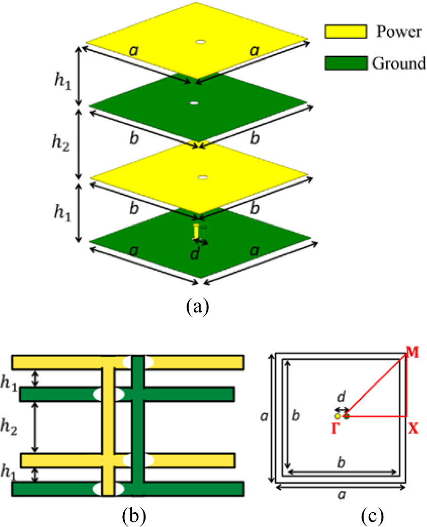
Figure 1: (a) The unit cell of the referenced EBG structure with (b) side view and (c) top view.
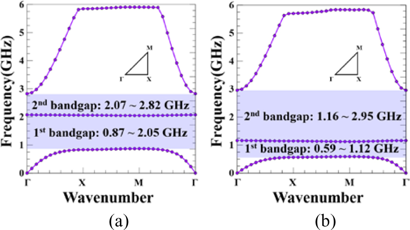
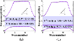
Figure 2: (a) The dispersion diagrams of the EBG cell of reference design and (b) that with thickened dielectric.
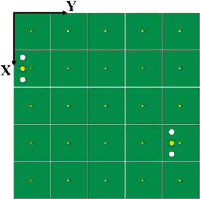
Figure 3: The structure with 5 5 EBG cells.
II. DESIGN CONCEPT AND PROCEDURE
A Suppression of propagation mode by discontinuity of impedance between plane pairs
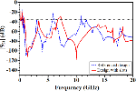
The reference design shown in Figure 1 is based on the EBG cell [7] with geometrical parameters (a, b, d, h, h) = (12 mm, 11.8 mm, 0.8 mm, 0.1 mm, 0.1 mm) for the PCB made of FR-4 material with relative permittivity = 4.4. The interleaved patches are double stacked in a four-layer stack-up. All the thicknesses of dielectric as well as the capacitance between adjacent planes are the same in the reference design. In order to extend the stopband bandwidth to lower frequency, the thickness of the dielectric, h, between the second and the third layers is increased from 0.1 to 0.8 mm. Therefore, the via barrel is lengthened and the inductance of the via is increased accordingly. As the capacitances between the first and second layers and the third and fourth layers remain the same, the increased inductance shifts the resonant frequency to lower frequency for extending the stopband bandwidth. The thickened dielectric between the second and the third layers also decreases the capacitance and results in the impedance discontinuities, so that the isolation for suppression of the noise propagation is enhanced. Figure 2 shows dispersion diagrams of the EBG cells of the reference design and that with thickened dielectric, respectively. For the result of the reference design, the bandgap is over the frequency range from 0.87 to 2.82 GHz except a propagating mode at 2.06 GHz. The bandgap of the design with thickened dielectric is from 0.59 to 2.95 GHz and its propagation mode is moved from 2.06 to 1.14 GHz. A 5 5 cells EBG board shown in Figure 3 is used to further analyze the effectiveness of isolation for the practicality. The cavity noise is excited at (18 mm, 3 mm) and the observation point is at (42 mm, 51 mm). Figure 4 shows that the design with thickened dielectric not only moves the propagation mode from 2.06 to 1.14 GHz but also enhances the isolation for suppression of the noise propagation. The cavity noise is suppressed under35 dB from 0.53 to 5.77 GHz.
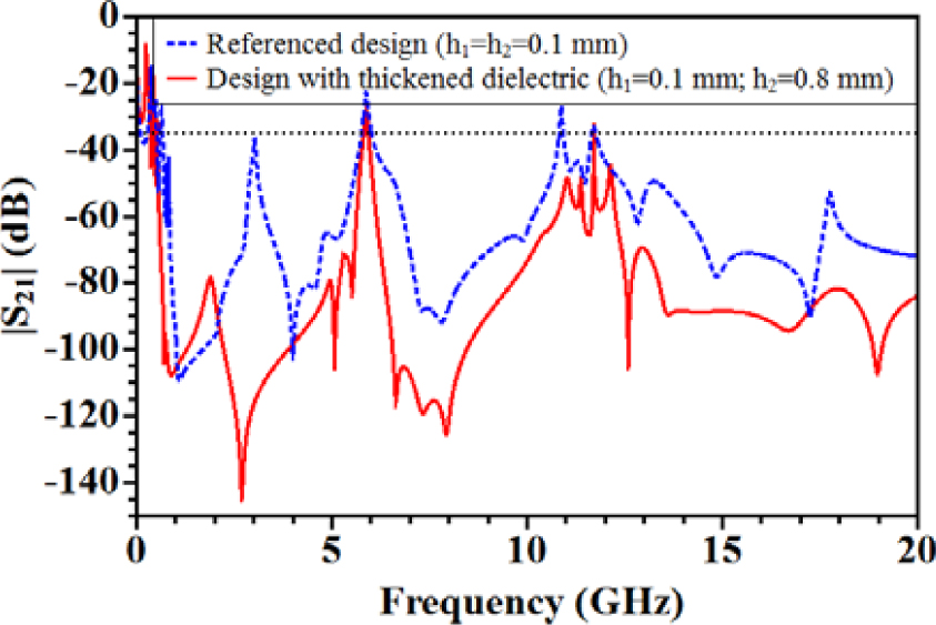
Figure 4: |S|of the structure with 5 5 EBG cells.

Figure 5: Patches of the EBG cell with slots.
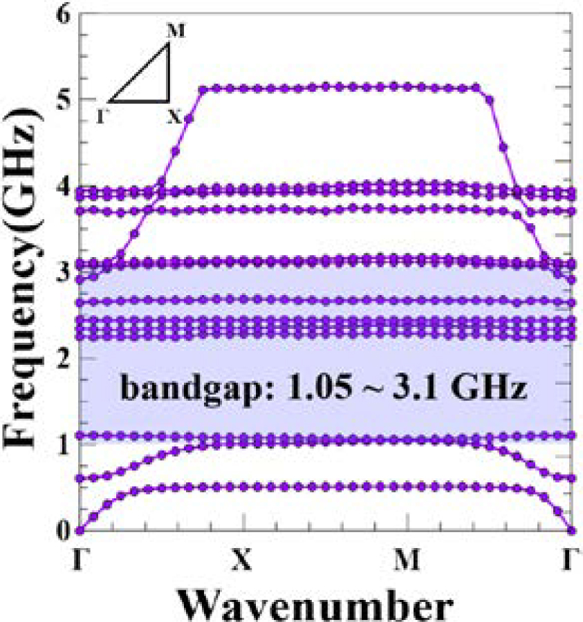
Figure 6: The dispersion diagrams of the EBG cell with slots.
B Suppression of propagation mode by patches with slots
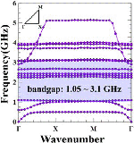
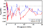
In order to suppress propagation modes for frequencies higher than 5.77 GHz, a novel EBG cell shown in Figure 5 is proposed for extending stopband bandwidth by excited multiple modes. The patches for the design shown in Figure 1 with geometrical parameters (a, b, d, h, h) = (12 mm, 11.8 mm,0.8 mm, 0.1 mm, 0.1 mm) are replaced by the proposed EBG cells with geometrical parameters (g, w) = (0.1 mm, 0.2 mm).The slots need to be located at the edges of the patch as the resonances are created by the inductance of the slot and the capacitance between patches. If the slots are close to the center of the patch, currents on the patch will directly flow through the via and the resonant modes will not be excited. Figure 6 shows the dispersion diagram of the EBG cells with slots. The bandgaps of the design with slots and that of reference design shown in Section II-A are alike, but multiple modes excited between 2 and 4 GHz shift the propagation mode from 5.9 to 7.2 GHz as Figure 7. As the propagation mode at 7.2 GHz still limits the stopband bandwidth, the structure comprises EBG cells with slots and the design of discontinuity of impedance between plane pairs is proposed in Section III.
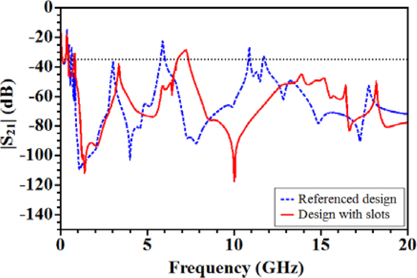
Figure 7: S|of the structure made of 5 5 EBG cells with slots.
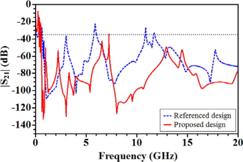
Figure 8: S|of the proposed structure with 5 5 EBG cells.
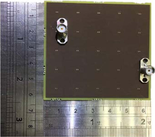
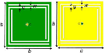
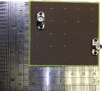
Figure 9: Top side of the experiment board.
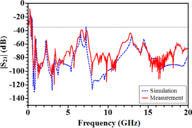
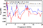
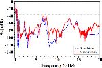
Figure 10: S|correlation between simulation and measurement.
III. SUPPRESSION OF NOISE PROPAGATION BY THE PROPOSED EBG STRUCTURE
The proposed structure is composed of slots on patches with thickened dielectric design for broadband suppression of noise propagation. The thickened dielectric is intended for the enhancement of noise isolation at low frequencies and the slots are responsible for the suppression of high frequency noise by excited multiple modes. Figure 8 shows the proposed structure can effectively suppress the cavity noise under 35 dB over the frequency range from 0.56 to 20 GHz. An experiment board shown in Figure 9 is designed for the validation of the proposed structure. 5 5 EBG cells are placed on a four-layer PCB with 6 cm 6 cm substrate. The cavity noise is injected and picked by two compression-mount SMA connectors, respectively. Figure 10 shows excellent correlation result between simulation and measurement. The measurement result proves the cavity noise can be suppressed under 35 dB from 0.56 GHz to the highest measurement frequency, 20 GHz.
IV. CONCLUSION
The cavity noise propagating between two planes can be picked by layer transition vias passing through the cavity. In this paper, an EBG structure based on interleaved and double stacked patches is proposed to suppress the cavity noise. The increased inductance of the proposed EBG cell shifts the resonant frequency to lower frequency and the multiple modes excited by additional slots shift propagation mode to higher frequency. The stopband bandwidth is then extended for the broadband suppression of the cavity noise. The simulation and measurement results indicate that the cavity noise is suppressed under 35 dB from 0.56 GHz to the highest measurement frequency, 20 GHz.
ACKNOWLEDGMENT
This work was supported in part by the Ministry of Science and Technology of Taiwan, and in part by the Inventec Corporation.
REFERENCES
[1] L. D. Smith and E. Bogatin, “Taming signal integrity problems when signals change return planes,” Principles of Power Integrity for PDN Design, 1st ed., Prentice Hall, Boston, Massachusetts, USA, pp. 363-426, 2017.
[2] K. Koo, L. G. Romo, T. Wang, T. Michalka, and J. Drewniak, “Fast decap assignment algorithm for optimization of power distribution networks,” 2017 IEEE International Symposium on Electromagnetic Compatibility & Signal/Power Integrity (EMCSI), Washington, DC, pp. 573-578, 2017.
[3] T. Wu, Y. Lin, and S. Chen, “A novel power planes with low radiation and broadband suppression of ground bounce noise using photonic bandgap structures,” IEEE Microwave and Wireless Components Letters, vol. 14, no. 7, pp. 337-339, Jul. 2004.
[4] C. Wang, G. Shiue, W. Guo, and R. Wu, “A systematic design to suppress wideband ground bounce noise in high-speed circuits by electromagnetic-bandgap-enhanced split powers,” IEEE Transactions on Microwave Theory and Techniques, vol. 54, no. 12, pp. 4209-4217, Dec. 2006.
[5] F. de Paulis, L. Raimondo, and A. Orlandi, “IR-DROP analysis and thermal assessment of planar electromagnetic bandgap structures for power integrity applications,” IEEE Transactions on Advanced Packaging, vol. 33, no. 3, pp. 617-622, Aug. 2010.
[6] J. Park, A. C. W. Lu, K. M. Chua, L. L. Wai, J. Lee, and J. Kim, “Double-stacked EBG structure for wideband suppression of simultaneous switching noise in LTCC-based SiP applications,” IEEE Microwave and Wireless Components Letters, vol. 16, no. 9, pp. 481-483, Sep. 2006.
[7] C. Wang and T. Wu, “Model and mechanism of miniaturized and stopband-enhanced interleaved EBG structure for power/ground noise suppression,” IEEE Transactions on Electromagnetic Compatibility, vol. 55, no. 1, pp. 159-167, Feb. 2013.
[8] G. Ouyang, X. Ye, and T. Nguyen, “Switching voltage regulator noise coupling to signal lines in a server system,” 2010 IEEE International Symposium on Electromagnetic Compatibility, Fort Lauderdale, FL, pp. 72-78, 2010.
[9] V. S. Pandit, W. H. Ryu, and M. Choi, “Signal/power integrity interactions,” Power Integrity for I/O Interfaces: With Signal Integrity/Power Integrity Co-Design, 1st ed., Prentice Hall, Boston, Massachusetts, USA, pp. 233-284, 2011.
BIOGRAPHIES

Ding-Bing Lin received the M.S. and Ph.D. degrees in electrical engineering from National Taiwan University, Taipei, Taiwan, in 1989 and 1993, respectively.
From 1993 to 2016, he was a Faculty Member with the Department of Electronic Engineering, National Taipei University of Technology, Taipei, Taiwan, where he was an Associate Professor, Professor, and Distinguished Professor in 1993, 2005, and 2014, respectively. Since August 2016, he has been a Professor with the Department of Electronic and Computer Engineering, National Taiwan University of Science and Technology.
Dr. Lin was the Chair of the Taipei Chapter, IEEE Broadcasting Society, from 2010 to 2014, the Technical Program Committee Chair of the 2015 Asia-Pacific International EMC Symposium, and the Chair of the Taipei Chapter, IEEE EMC Society from 2015 to 2018. He has been an Associate Editor for the IEEE Transactions on EMC since 2019 and in the Editorial Board of the International Journal of Antennas and Propagation since 2014. He is currently directing a human resources cultivation program named the Promotion Center for 5G Antennas and Radio Frequency Techniques Consortium. He has authored or coauthored more than 200 papers in international journals and at international conferences, respectively. His research interests include wireless communication, radio multipath fading channel modeling, mobile antennas, high-speed digital transmission, and microwave engineering.

Yen-Hao Chen received the M.S. degree in computer, communication, and control engineering from the National Taipei University of Technology, Taipei, Taiwan, in 2003. He is currently working toward the Ph.D. degree in electronic and computer engineering with the National Taiwan University of Science and Technology, Taipei, Taiwan.
He has been working with Inventec Corporation since 2003 where his responsibilities include the design and analysis of signal and power integrity for products of servers, network switches, and storage equipment. His research interests include SI/PI simulations and noise modeling of switched-mode power supply.

Min-Hung Hsieh received the M.S. degree in electronic and computer engineering from the National Taiwan University of Science and Technology, Taipei, Taiwan, in 2018.
He has been working with Inventec Corporation since 2019 where his responsibilities include the design and analysis of signal integrity for industrial servers. His current interests include SI/PI simulations for PCIe and DDR signals.
ACES JOURNAL, Vol. 37, No. 5, 619–623.
doi: 10.13052/2022.ACES.J.370511
© 2021 River Publishers