A Compact Bandstop Filter Design Using DMS-DGS Technique for Radar Applications
Burak Dokmetas1, Galip Orkun Arican2, Nursel Akcam1, and Erdem Yazgan3
1Department of Electrical and Electronics Engineering, Gazi University, Ankara, Turkey
burakd@gazi.edu.tr, ynursel@gazi.edu.tr
2ASELSAN Inc., Communication and Information Technologies Division, Ankara, Turkey
goarican@aselsan.com.tr
3Department of Electrical and Electronics Engineering, TED University, Ankara, Turkey
erdem.yazgan@tedu.edu.tr
Submitted On: June 7, 2021; Accepted On: October 18, 2021
Abstract
In this study, a novel compact bandstop filter (BSF) by utilizing the defected ground structure (DGS) and defected microstrip structure (DMS) techniques are presented. DGS, DMS, and compensated capacitors are used on both bottom and top layers to obtain sharp transition and wider stopband. The operating frequency bandwidth of the filter can be comfortably regulated by tuning the dimensions of the etched structures. In addition to parametric studies, an equivalent circuit model of the proposed filter is extracted. The BSF has an insertion and return losses better than –1.6 and –17 dB in the passband, respectively. Moreover, the developed filter covers X-band frequency range and has stop bandwidth of 10.8–11.8 GHz with the rejection of better than 20 dB. Furthermore, the measurement and simulation results are in compliance with the suggested method. The proposed BSF has a very small size of 14.28 mm 4 mm 0.508 mm and has the potential to be used for radar applications with its high compactness, low cost, and high harmonic rejection performance.
Index Terms: Bandstop filter (BSF), defected ground structure (DGS), X-band application.
I. INTRODUCTION
In recent years with the advancement of wireless communication and wireless power transfer technology, the requirement to microwave devices with high performances is increased. One of the most significant components of these devices are microwave filters. Microstrip filters are important passive elements for the attenuation of unwanted signals and noise in communication technology [1, 2]. Therefore, the development of compact and low cost microstrip filters with out-of-band rejection feature is getting more attention in modern communication systems. So to accomplish these requirements, many filtering structures have been investigated [3].
In addition, several defected ground structure (DGS) studies for microstrip applications have been reported during these decades. The DGS is realized by adding defected resonator on the ground plane to change the values of the distributed capacitance and inductance of the transmission line [4, 5]. In the previously reported studies, DGS technique was implemented to miniaturize the circuit size. In addition, a miniaturization up to 50% was reported by using DGS technique in the literature [6]. Moreover, a miniaturized dual-band triangle-shaped DGS bandstop filter (BSF) for energy harvesting applications is fabricated [7]. Furthermore, resonant frequency can be controlled by changing the dimension and shapes of the etched slots [8, 9]. This technique is evitable for both periodic and non-periodic structures.
Defected microstrip structure (DMS) is realized by etching specific slots in the transmission line and it exhibits the properties of slow wave [10]. The bandstop response and selectivity behaves are akin to the DGS but without any damage on the ground plane. As opposed to the DGS technique, the frequency response of the DMS structure is almost the same when the microstrip length varies [11]. Moreover, in the literature, it is reported that DMS and DGS techniques are used at the same time for different microwave applications. T-shaped DMS and U-shaped DGS were used to create dual-band BSF [12]. Hexagonal fractal antenna was designed for UWB applications based on DGS-DMS technique [13]. A bandpass filter with narrow bandwidth for WLAN applications was fabricated [14].
In this study, a novel compact microstrip BSF for X-band application is proposed. The prominent features of this study are the usage of DGS-DMS technique to accomplish a much more compact structure with a unique design compared to the studies in the literature and the development of the equivalent circuit model (ECM) to be able to design higher order filters. In addition, a three-stage design procedure is presented to explain the proposed topology. In the first stage, the characteristics of the suggested modified meander DGS shape are analyzed. In the second stage, the effects of the rectangular DMS shapes on frequency response are investigated. In the final stage, the compensated capacitors are added on the strip line. Moreover, an ECM of the final design is extracted based on lumped elements [15] and the values of each circuit component is theoretically calculated. Agilent ADS circuit simulator is used to simulate the ECM results and CST software is used for 3D electromagnetic (EM) analysis. Furthermore, the BSF is modeled and manufactured on a Rogers RT5880 substrate with a dielectric constant of 2.2 and electric loss tangent of 0.0009. Substrate and copper metallization thicknesses are chosen as 0.508 and 0.035 mm, respectively. The proposed filter has a compact size compared to reported works with an area of 57.12 mm.
II. MICROSTRIP FILTER DESIGN
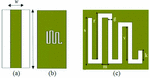
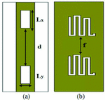
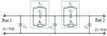
In the first stage, the two layered filter design with meandered DGS slot is presented. On the top layer, there is a transmission line, whose characteristic impedance is 50 with a width of w = 1.6 mm. In addition, on the bottom layer, the proposed meandered DGS slot is etched on the ground plane. Figure 1 shows the detailed layouts of the proposed filter (Step-1).
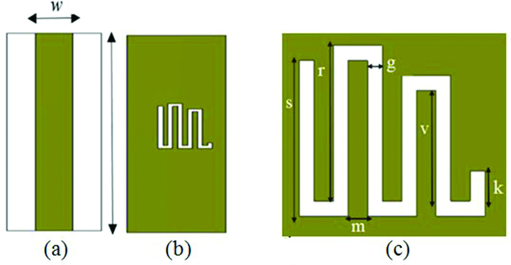
Fig. 1. Geometry of the microstrip filter design (Step-1). (a) Top layer. (b) Bottom layer. (c) Proposed DGS structure.
The 3D-EM simulation of the filter is performed using the CST Microwave Studio [16]. Table 1 shows the optimized values of the BSF (Step-1).
Table 1: Optimized dimensions of the filter
| Parameter | Value (mm) | Parameter | Value (mm) |
| w | 1.60 | d | 6.10 |
| l | 14.50 | f | 1.10 |
| k | 0.20 | L | 0.80 |
| m | 0.20 | L | 2.90 |
| v | 2.54 | W | 0.40 |
| g | 0.20 | W | 1.80 |
| s | 3.10 | p | 0.50 |
| r | 3.10 | p | 7.40 |
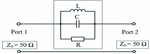
The DGS ensures a cutoff frequency (f) and attenuation pole frequency (f). Cutoff frequency is defined as the frequency where the insertion loss is 3 dB below the passband. Attenuation pole can be achieved with the combination of inductance and capacitance elements. Therefore, the equivalent circuit of the DGS unit can be formulated by an RLC network [15] as shown in Figure 2. In addition, the frequency-independent components are utilized to simplify the ECM to be able to easily design a higher order filters up to Ku-band. However, there would be slight discrepancies at the frequency band that is higher than X-band.
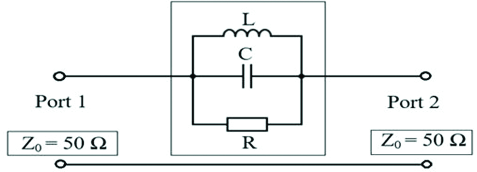
Fig. 2. Circuit model of the proposed DGS shape.
As investigated in [15], the microstrip line exhibits bandstop response by using DGS section and its frequency characteristics can be calculated with effective inductance and capacitance using the following equations:
| (1) |
| (2) |
| (3) |
Z denotes the characteristic impedance of the transmission line in this equation. According to the equations, R, L, and C are calculated as 4.4 k, 0.26 nH, and 0.82 pF, respectively.
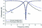
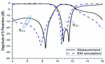
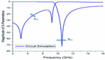
Figure 3 shows the ECM and full wave EM simulation results. As shown in the figure, the ECM results show a unison with the EM simulation results at “f= 10.81 GHz” and “fc = 9.8 GHz.” On the other hand, a slight discrepancy has observed above 11 GHz. These discrepancies can be caused by the frequency-independent components in the ECM.
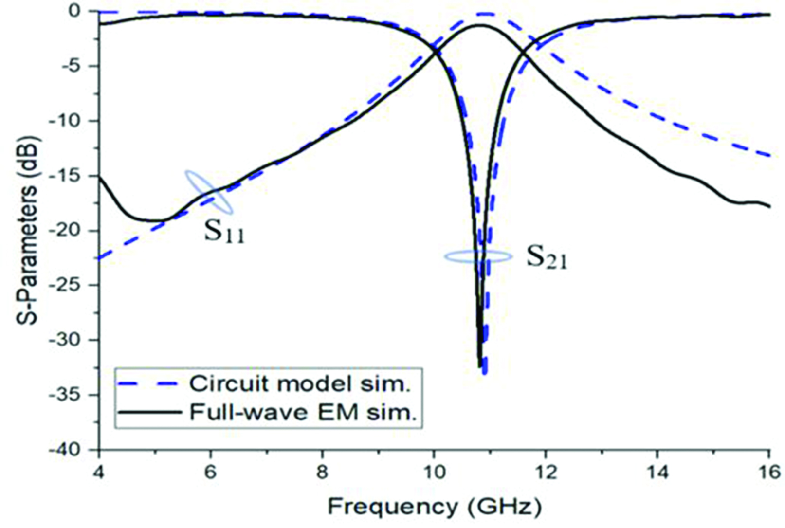
Fig. 3. Comparison between circuit model and EM simulation of the proposed microstrip filter (Step-1).
III. PARAMETRIC STUDY
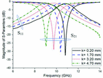
So to investigate the response of different dimensions on the resonator, parametric analysis of the design of Step-1 is carried out. Figure 4 shows the effect of various dimensions of “k” on S-parameters. At this stage, “k” changes while other parameters remain constant. As observed in Figure 4, with the increase of “k,” the insertion loss shifts to the lower frequency band.
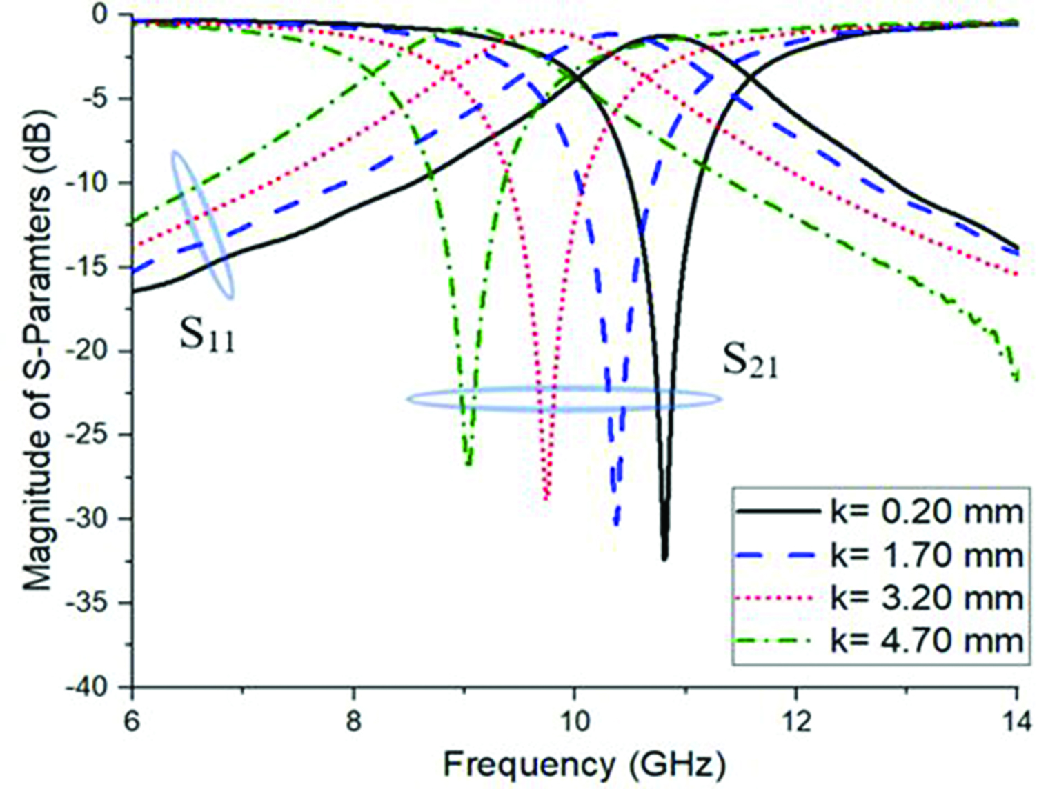
Fig. 4. Simulated S-Parameter results for different k values.
The obtained results for different “k” values are calculated and summarized in Table 2. As observed in Table 2, with the increase of “k,” the maximum point of the insertion loss (S), f, and f decreases. Moreover, the capacitance and resistance decrease with the increase of “k,” while inductance increases. Moreover, the same procedure was similarly done for the other parameters and the obtained results were summarized in Tables 3 and 4.
Table 2: Effect of the proposed DGS shape with different k values (m = 0.2 mm; g = 0.2 mm)
| k (mm) | f (GHz) | f (GHz) | S (dB) |
| 0.20 | 10.81 | 9.88 | –32.79 |
| 1.70 | 10.36 | 9.38 | –30.04 |
| 3.20 | 9.74 | 8.73 | –28.94 |
| 4.70 | 9.03 | 8.06 | –27.12 |
| BW (GHz) | L (nH) | C (pF) | R (k) |
| 0.18 | 0.26 | 0.82 | 4.40 |
| 0.19 | 0.30 | 0.77 | 3.27 |
| 0.18 | 0.35 | 0.74 | 2.85 |
| 0.22 | 0.40 | 0.77 | 2.15 |
According to Table 3, the length of “m” is increased with a period of 0.2 mm and the obtained changes are investigated. The results show that the increase of “m” causes a decrease in f, f, S, and stopband width (BW). In addition, inductance increases from 0.26 to 0.64 nH in this period. Capacitance and resistance values are in downward trend.
According to Table 4, it is interpreted that the increase of “g,” the width of the proposed DGS pattern, causes almost no change on f except the g = 0.1 mm dimension. Further f, resistance, and capacitance values are decreasing with the increase of “g” dimension. However, inductance and BW progressively increase. It is obvious from Table 4 that by tuning the “g” dimension, the desired attenuation pole frequency can be obtained.
Table 3: Effect of the proposed DGS shape with different m values (k = 0.2 mm, g = 0.2 mm)
| m (mm) | f (GHz) | f (GHz) | S (dB) |
| 0.20 | 10.81 | 9.88 | –32.79 |
| 0.40 | 9.54 | 8.18 | –24.58 |
| 0.60 | 7.62 | 6.46 | –12.24 |
| 0.80 | 6.93 | 5.80 | –12.04 |
| BW (GHz) | L (nH) | C (pF) | R (k) |
| 0.18 | 0.26 | 0.82 | 4.40 |
| 0.25 | 0.54 | 0.51 | 1.86 |
| 0 | 0.63 | 0.69 | 0.65 |
| 0 | 0.64 | 0.82 | 0.34 |
Table 4: Effect of the proposed DGS shape with different g values (m = 0.2 mm; k = 0.2 mm)
| g (mm) | f (GHz) | f (GHz) | S (dB) |
| 0.1 | 10.16 | 9.77 | –25.51 |
| 0.2 | 10.81 | 9.88 | –32.79 |
| 0.3 | 10.81 | 9.32 | –32.42 |
| 0.4 | 10.86 | 8.53 | –28.09 |
| BW (GHz) | L (nH) | C (pF) | R (k) |
| 0.04 | 0.12 | 2.00 | 3.95 |
| 0.18 | 0.26 | 0.82 | 4.40 |
| 0.28 | 0.46 | 0.45 | 3.86 |
| 0.44 | 0.70 | 0.30 | 2.73 |
IV. DGS-DMS BANDSTOP FILTER: DESIGN CONCEPT
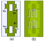
The DGS-DMS BSF configuration is presented in this stage (Step-2). As shown in Figure 5, the filter design consists of two 0.8 mm 2.9 mm identical rectangular DMS shapes which are placed with 6.1 mm distance on the strip line. These resonators are connected to connectors with the transmission line. The rectangular DMS structures behave as a bandstop element. This is an intended response from the filter. With this approach, the desired band stopping feature is achieved in the desired X-band frequency range.
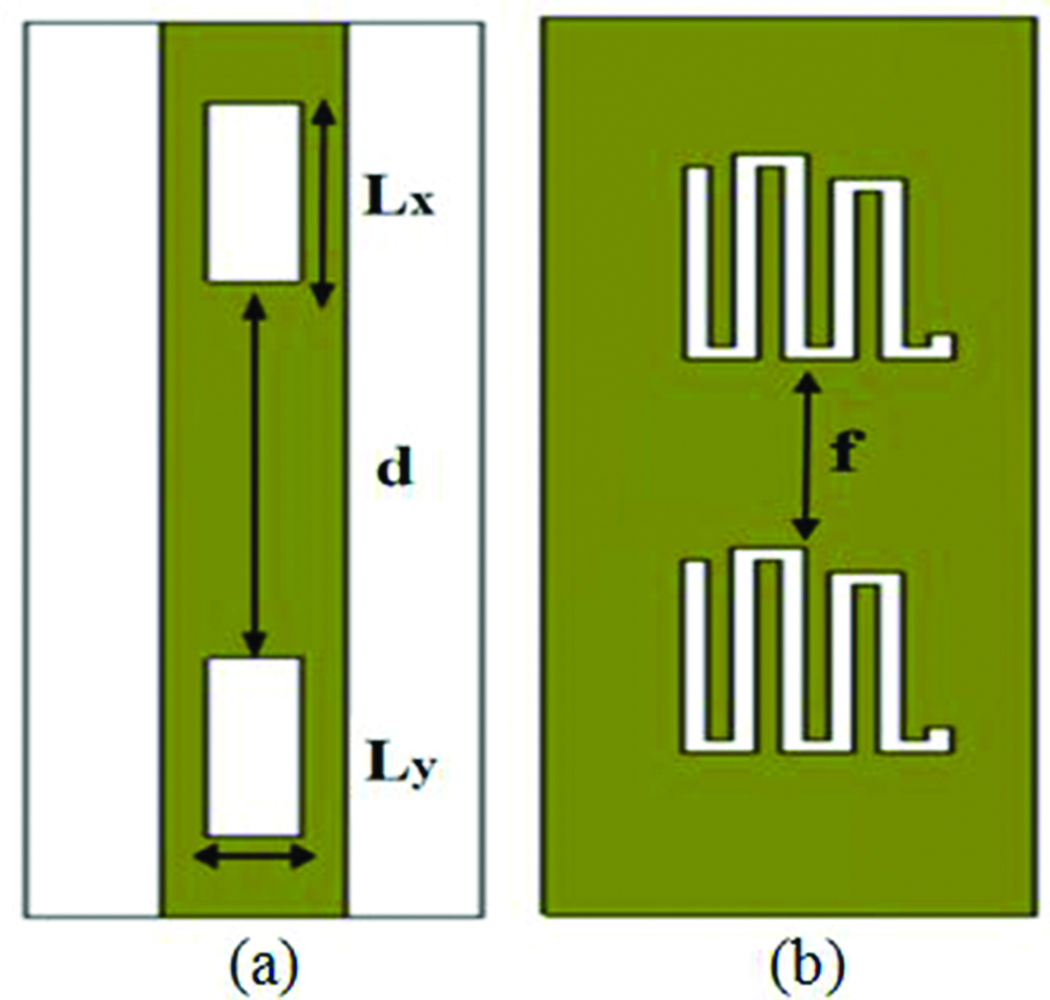
Fig. 5. Layout of the DMS-DGS structure (Step-2): (a) top layer; (b) bottom layer.
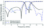
In order to test the accuracy of the proposed model, the EM simulation result and the measurement results were compared. As shown in Figure 6, by using the combination of two rectangular DMS and two identical DGS shapes, there occurs a BSF behavior with 960 MHz stopband width (SBW).
In these results, the situation that can be evaluated as negative is the passband region between 4–8 GHz and 12–16 GHz. This issue will be discussed in the next section.
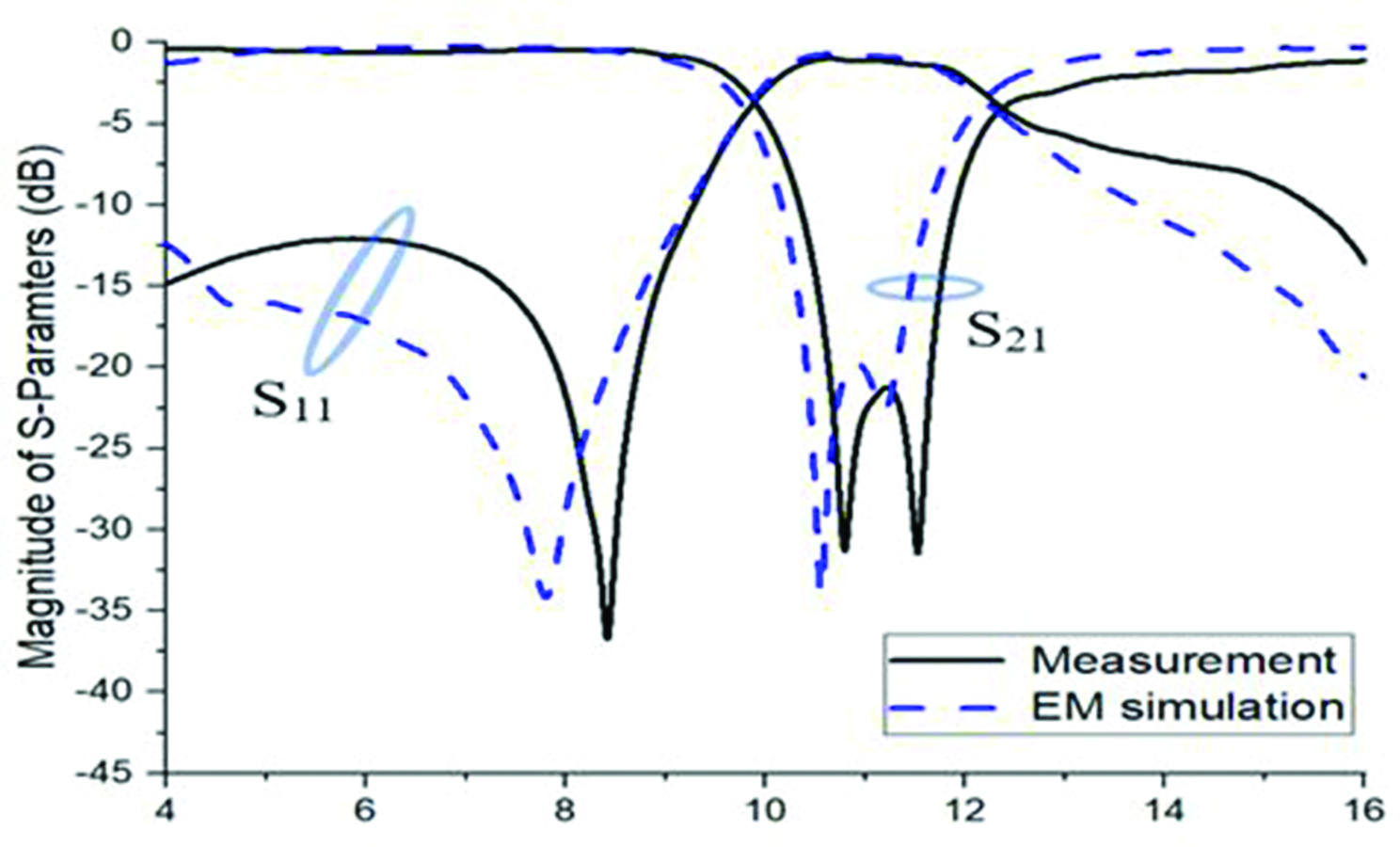
Fig. 6. Comparison of simulated and measured results of DMS-DGS bandstop filter (Step-2).
V. BSF USING COMPENSATED CAPACITORS
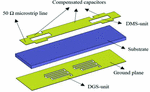
In order to enhance the performance of the passband of the filter Step-2, three compensated capacitors are added as shown in Figure 7. This new final design is called Step-3. The two DMS shapes and the added parallel microstrip capacitors are directly connected with the SMAs. Figure 8 shows the 3D layout of the proposed BSF filter.
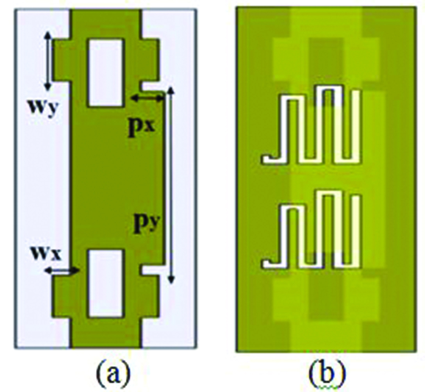
Fig. 7. Layout of the final bandstop filter structure: (a) top layer; (b) bottom layer.
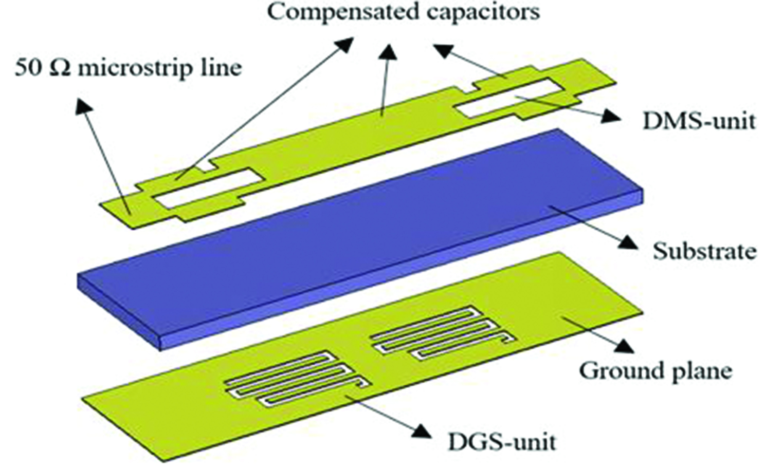
Fig. 8. 3D layout of the proposed bandstop filter.
Figure 9 indicates the comparison of the EM simulation results of the designed filters in Step-2 and Step-3. In the EM simulation results, it is seen that insertion loss characteristics of Step-2 and Step-3 are almost similar to each other. On the other hand, Step-3 has a better bandpass performance in the frequency bandwidths of 4–7.1 GHz and 12.2–16 GHz. The added conductors with the size (w w and p p) on the strip line allows to increase the coupling capacitance between 50 microstrip line and proposed DGS shape [17]. For this reason, the characteristic of the filter is related to the physical dimensions of the added capacitors and DGS shape.
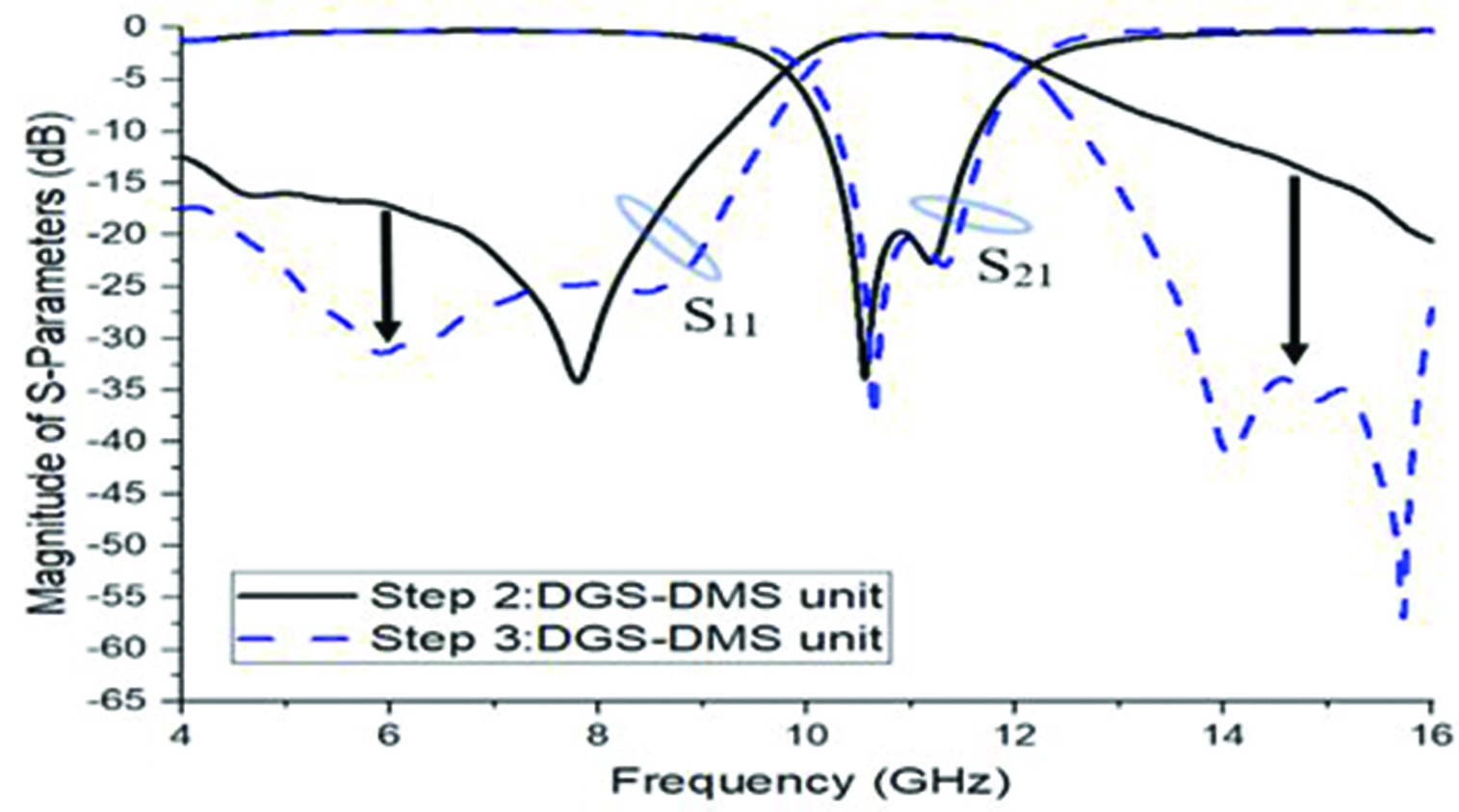
Fig. 9. Comparison of simulated results of the structures presented in Step-2 and Step-3.
According to the proposed theory, the proposed BSF can be modeled as two cascaded DGS shapes along with three shunt capacitors Cand C. Figure 10 represents the equivalent circuit of the proposed BSF. In the design, two identical DGS shapes are used to enhance the stopband rejection attributions of the filter. The values of the L, C, and R parameters were extracted by utilizing eqn (1)–(3), which were explained in Section II. The equivalent capacitance can be obtained from [18] as
| (4) |
In this equation, Z, l, l, w, , and correspond to characteristic impedance, physical length of the added capacitor, physical width of the series reactance, width of the added capacitance, and guided wavelengths, respectively. From this equation, the values of Cand C were calculated as 0.04 and 0.3 pF, respectively. Figure 11 shows the S-parameter results of the extracted ECM. The circuit model simulation results are unison with the EM results in the 4–12 GHz frequency bandwidth. However, there is a difference in the higher frequency (12 GHz). The difference between the equivalent model and measurement results in the higher frequencies can be caused by the frequency-independent components that are utilized in the ECM.
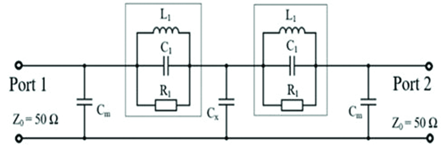
Fig. 10. Equivalent circuit model of the BSF.
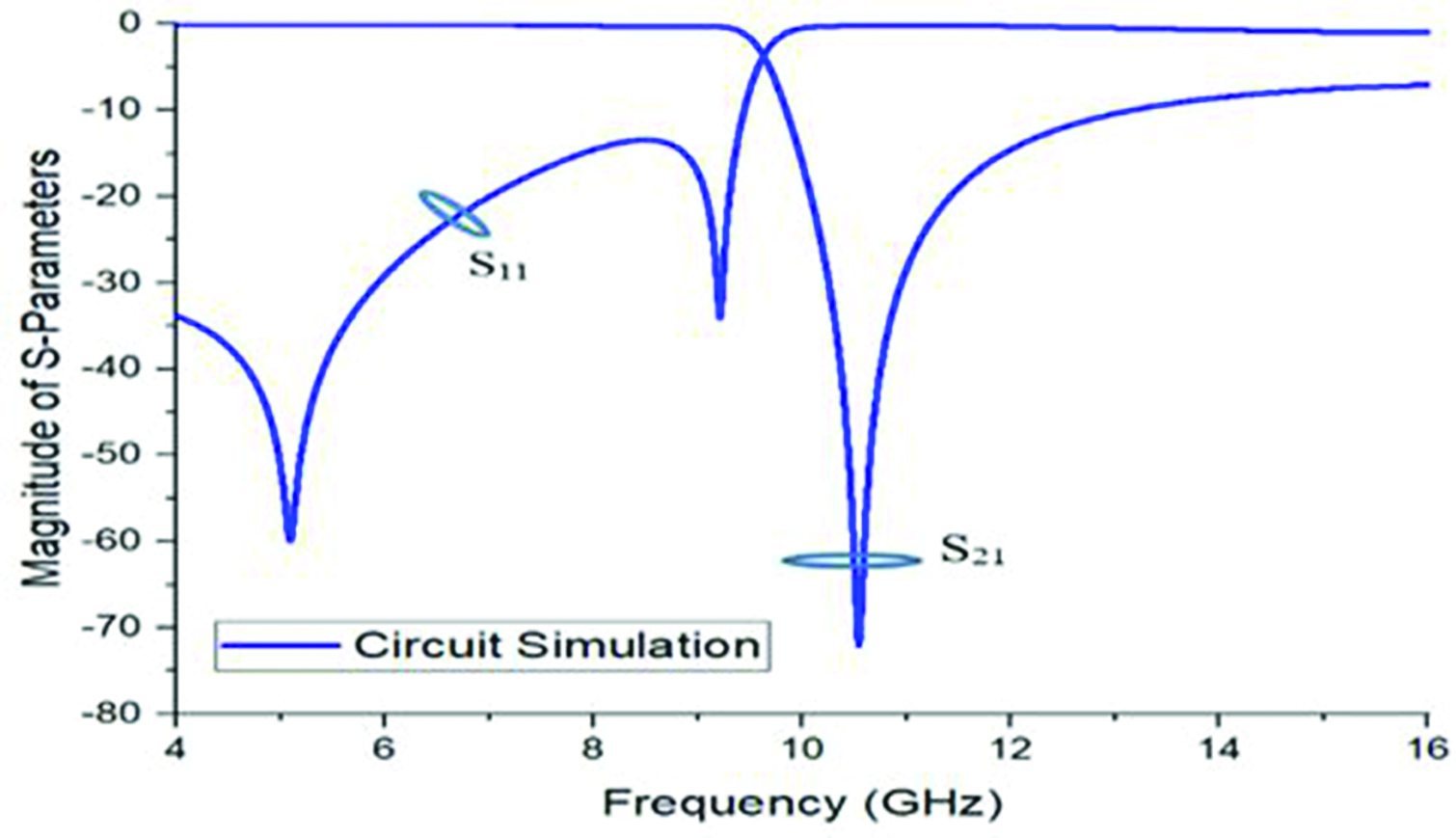
Fig. 11. S-parameter results of the circuit model.
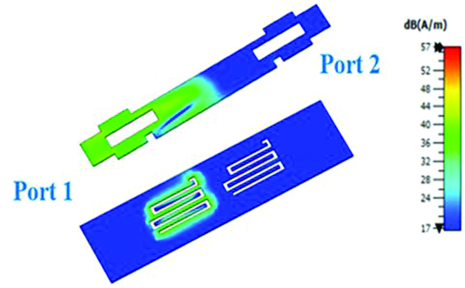
Fig. 12. EM field distribution results at 11 GHz (stopband).
The magnetic field distribution of the proposed filter was investigated for the passband frequency of 6 GHz and stopband frequency of 11 GHz. As noticed from Figure 12, the current is mainly concentrated along the edges of the modified meander DGS pattern. The green color illustrates large values, whereas the blue color illustrates the small values of the magnetic field. The signal is blocked in Port 1 (the input feed port) on the stopband region at 11 GHz, with no energy flow around port 2. The field was mainly focused over one DGS element as two identical electric and magnetic energies [19]. On the other hand, in passband region at 6 GHz, the RF power was transmitted from port 1 to port 2 as shown in Figure 13. The magnetic-field patterns declare compatible coupling between the feeds and the DGS structures.
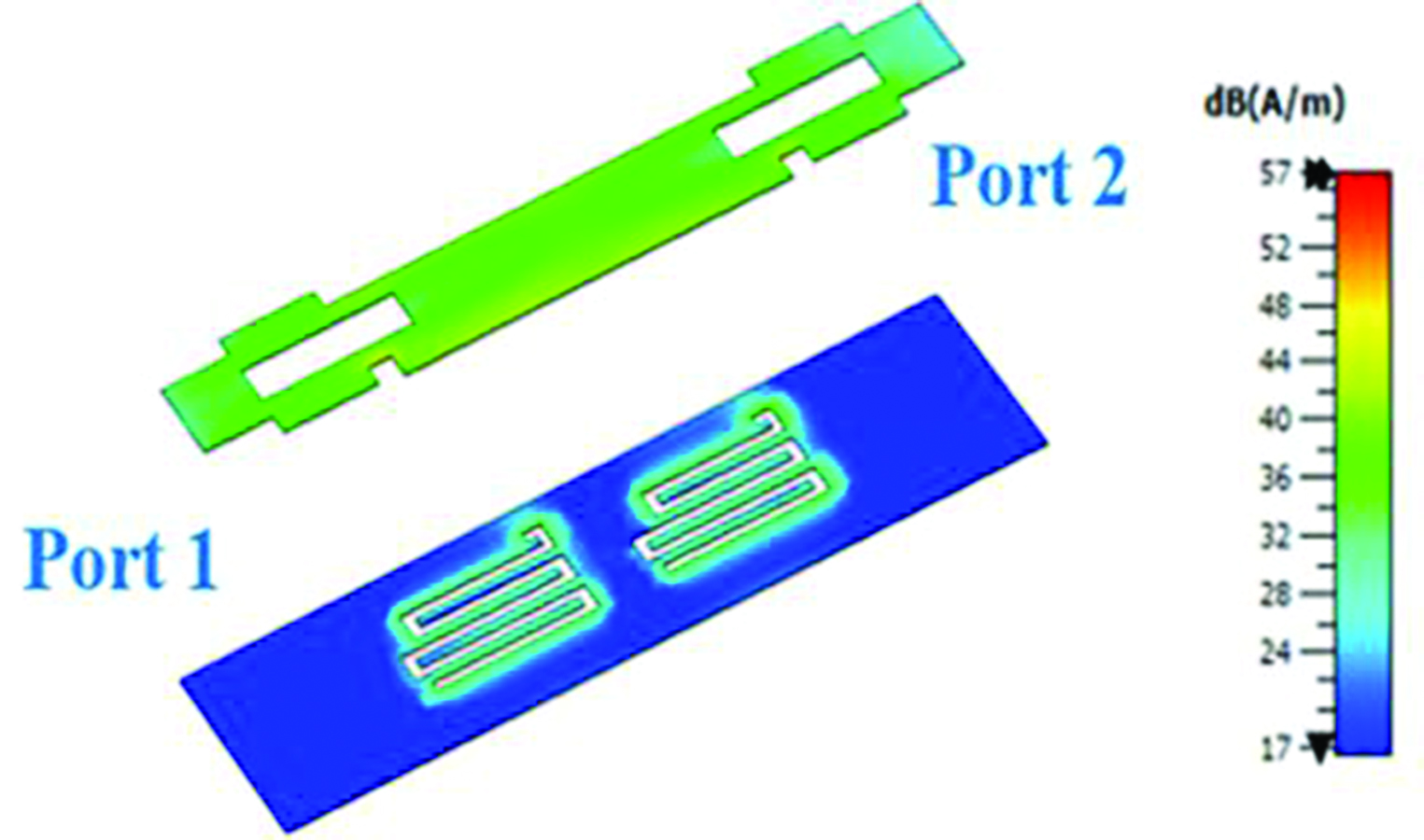
Fig. 13. EM field distribution results at 6 GHz (passband).
VI. FABRICATION AND MEASUREMENT
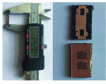
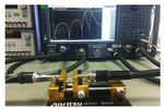
Figure 14 presents the photograph of the manufactured compact BSF. The S-parameter measurements were performed by utilizing Anritsu 3680K universal test fixture and Keysight N5224B Network Analyzer as shown in Figure 15.
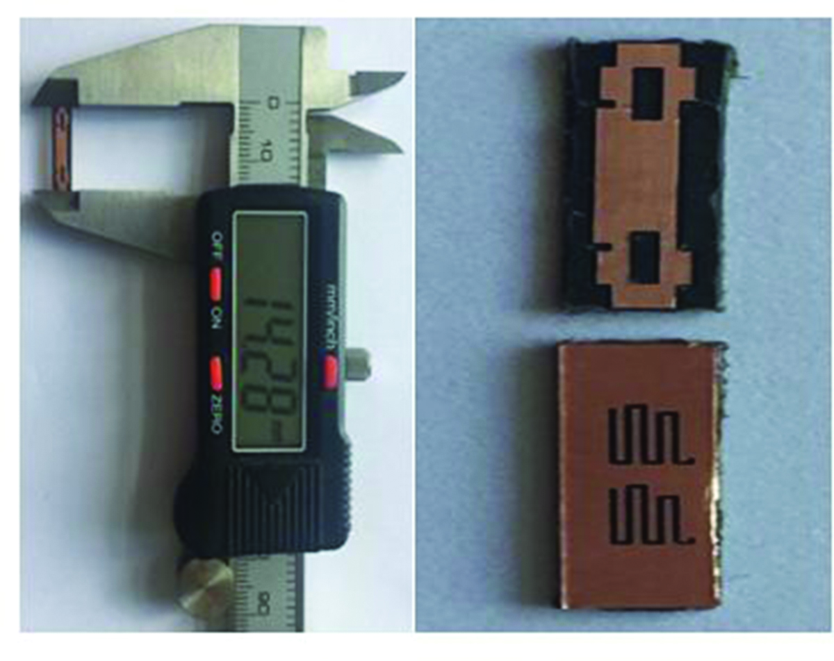
Fig. 14. Photograph of the manufactured DMS-DGS BSF.
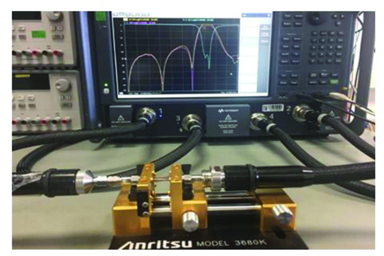
Fig. 15. Photograph of the measurement setup.
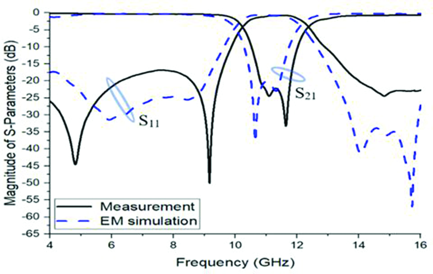
Fig. 16. Measured and simulated S-parameters of the proposed BSF (Step-3).
Table 5: Comparison of the designed BSF with the reported works
| Ref. | Area | SBW | RB | S | S | |
| no. | (mm) | (GHz) | (GHz) | (dB) | (dB) | E.C. |
| [20] | 210 | 0.5 | 1.1 | –20 | –24 | X |
| [21] | 150 | 3.3 | 4 | –10 | –19 | X |
| [22] | 150 | 2.6 | 5.3 | N/A | –27 | X |
| [23] | 90.11 | 2.55 | 4 | –15 | –52 | X |
| This work | 57.12 | 1 | 2 | –17 | –23 | X |
As shown in Figure 16, in the measurement, the suppression level of the proposed BSF filter (Step-3) was better than 20 dB in the frequency bandwidth of 10.8–11.8 GHz as given in Figure 16. The return loss (S) was less than –17 dB in the passbands. The measured S-parameter results were shifted approximately 250 MHz to higher frequencies with respect to the EM simulation results.
The detailed summary of different BSFs suggested for the same frequency range is listed in Table 5. N/A denotes “not available” and E.C denotes “equivalent circuit.”
The proposed filter has a very compact size of 57.12 mm with respect to other reported works. This work has the best |S| value except [20]. The insertion loss in stopband was compared and good results were achieved except [23]. The values in [23] include the simulation results. Rejection bandwidth (RB) is the bandwidth of insertion loss |S| at –3 dB and stopband bandwidth (SBW) is defined as the bandwidth of insertion loss |S| at –20 dB. The obtained SBW and RB values were suitable for X-band applications with its compact size. This work also focuses on circuit analysis in addition to the production and simulation of design.
VII. CONCLUSION
A novel design of bandstop microstrip filter has been presented. The gradual DMS-DGS technique in combination with added compensated capacitors was utilized to achieve the desired stopband characteristic. The results were shown that the proposed filter has a bandstop effect that includes from 10.3 to 12.3 GHz. A prototype of the proposed BSF was manufactured, and it was observed that EM simulation results are in compliance with the measurement results. Due its compactness, low cost, and high suppression performance, the proposed filter is a good candidate for radar applications.
ACKNOWLEDGMENT
The authors would like to thank ASELSAN Inc. for the support provided in the fabrication and measurement of the data used in this work.
REFERENCES
[1] D. Lu, M. Yu, N. S. Barker, Z. Li, W. Li, and X. Tang, “Advanced synthesis of wide-tuning-range frequency-adaptive bandpass filter with constant absolute bandwidth,” IEEE Trans. Microw. Theory Techn., vol. 67, no. 11, pp. 4362-4375, Nov. 2019.
[2] D. Psychogiou and R. Gomez-Garcia, “Multi-mode-cavity-resonator-based bandpass filters with multiple levels of transfer-function adaptivity,” IEEE Access, vol. 7, pp. 24759-24765, 2019.
[3] X. Cao, Z. X. Tang, and F. Wang, “A method of designing dual-band bandpass filter using the hexagon CRLH resonators and cascaded defected ground structure,” Microw. Opt. Technol. Lett., vol. 57, no. 8, pp. 1876-1879, Aug. 2015.
[4] Y. Han, Z. Liu, C. Zhang, C. Mei, Q. Chen, K. Hu, and S. Yuan, “A flexible microstrip low-pass filter design using asymmetric pi-shaped DGS,” IEEE Access, vol. 7, pp. 49999-50006, 2019.
[5] F.-C. Chen, H.-T. Hu, J.-M. Qiu, and Q.-X. Chu, “High-selectivity low-pass filters with ultrawide stopband based on defected ground structures,” IEEE Trans. Compon., Packag., Manuf. Technol., vol. 5, no. 9, pp. 1313-1319, Sep. 2015.
[6] H. Elftouh, N. A. Touhami, M. Aghoutane, S. E. Amrani, A. Tazon, and M. Boussouis, “Miniaturized microstrip patch antenna with defected ground structure,” Progress in Electromagnetics Research C, vol. 55, pp. 25-33, 2014.
[7] S. Verma, E. Sareen, and M. S. Hashmi, “A miniaturized dual-band right triangle defected ground structure band stop filter for energy harvesting applications,” in Proc. IEEE MTT-S Int. Microwave and RF Conf., Kolkata, India, pp. 1-3, 2018.
[8] A. Kumar and M. V. Kartikeyan, “Design and realization of microstrip filters with new defected ground structure (DGS),” Engineering Science and Technology, an International Journal., vol. 20, pp. 679-686, Apr. 2017.
[9] M. K. Khandelwal, B. K. Kanaujia, and S. Kumar “Defected ground structure: fundamentals, analysis, and applications in modern wireless trends,” International Journal of Antennas and Propagation, pp. 1-22, 2017.
[10] D. S. La, Y. H. Lu, S. Y. Sun, N. Liu, and J. L. Zhang, “A novel compact band stop filter using defected microstrip structure,” Microw. Opt. Technol. Lett., vol. 53, pp. 433-435, Feb. 2011.
[11] J. A. Tirado-mendez and H. Jardon-aguilar, “Comparison of defected ground structure (DGS) and defected microstrip structure (DMS) behavior at high frequencies,” Electrical and Electronics Engineering, 2004. (ICEEE). 1st International Conference, pp. 7-10, 2004.
[12] T. Praludi, Y. Y. Maulana, E. R. Yuliasih, D. P. Kurniadi, and Y. Taryana “Dual-band bandstop filter microstrip using T-DMS and U-DGS,” 2019 International Conference on Radar, Antenna, Microwave, Electronics, and Telecommunications (ICRAMET), 2019.
[13] D. Upadhyay, I. Acharya, and A. K. Gupta, “DGS & DMS based hexagonal fractal antenna for UWB applications,” 2015 International Conference on Communications and Signal Processing (ICCSP), pp. 0176-0179, 2-4 Apr. 2015.
[14] A. Kumar and M. V. Kartikeyan, “A design of microstrip bandpass filter with narrow bandwidth using DGS/DMS for WLAN,” IEEE Conference Publications, 2013.
[15] X. Chen, L. Wang, L. Weng, and X. Shi, “Compact low pass filter using novel elliptic shape DGS,” Microwave Opt Technol Lett., vol. 51, pp. 1088-1091, 2009.
[16] CST Microwave Studio, ver. 2008, Computer Simulation Technology, Framingham, MA, 2008.
[17] A. Boutejdar, A. A. Ibrahim, and E. P. Burte, “Design of a novel ultrawide stopband lowpass filter using a DMS-DGS technique for radar applications,” International Journal of Microwave Science and Technology., Article ID 101602, Hindawi Publishing Corporation, 2015.
[18] J. S. Hong and M. J. Lancaster, Microstrip Filters for RF/Microwave Applications. John Wiley & Sons, Inc., New York, 2001.
[19] M. Challal, A. Boutejdar, and A. Azrar, “Design of compact low-pass filter with large reject band using open circuit stubs and two cascaded DGS quasitriangular resonator,” Microwave Opt Technol Lett., vol. 55, pp. 122-127, 2013.
[20] B. Shrestha and N.-Y. Kim, “Compact and miniaturized bandstop filter developed using slot spurline technique,” Microwave and Optical Technology Letters, vol. 56, no. 5, pp. 1029-1031, Mar. 2014.
[21] H. Keivani, N. Adlband, and Y. Ojaroudi, “Compact band-stop X-band filter using triple meander-line-ring defected ground structures,” Applied Computational Electromagnetics Society (ACES) Journal, vol. 30, no. 8, Aug. 2015.
[22] M. Pourbagher, N. Ojaroudi, C. Ghobadi, and J. Nourinia, “Compact band-stop filter for X-band transceiver in radar applications,” Applied Computational Electromagnetics Society (ACES) Journal, vol. 30, no. 4, Apr. 2015.
[23] A. O. Ertay, and S. Simsek, “A compact bandstop filter design for X-band applications,” International Symposium on Fundamentals of Electrical Engineering (ISFEE), IEEE, June 30-July 2, 2016.
BIOGRAPHIES

Burak Dokmetas received the B.S. degree in electrical and electronic engineering from Inonu University, Malatya, Turkey, in 2010, and the M.S. degree in electrical and electronic engineering from Gazi University, Ankara, Turkey, in 2016. He is currently working toward the Ph.D. degree in electrical and electronic engineering with the Gazi University.
His main interests are microwave antennas, microwave filters, electromagnetic theory, and radar systems.

Galip Orkun Arican received the B.S. degree from Bilkent University, Ankara, Turkey, in 2010, the M.S. degree from Middle East Technical University, Ankara, Turkey, in 2014, and the Ph.D. degree from Gazi University, Ankara, Turkey, in 2021.
From 2010 to 2015, he worked as a MMIC Design Engineer with Nanotechnology Research Center, Bilkent University. Since 2015, he has been working as a RF/Microwave Design Engineer with ASELSAN Inc. His research interests include high frequency applications, GaN/GaAs MMICs, satellite communication, microwave antennas, filters, and electromagnetic theory.
Nursel Akcam received the M.S. and Ph.D. degrees in electrical and electronics engineering from the University of Gazi, Ankara, Turkey, in 1993 and 2001, respectively.
She has been a Professor of Electrical and Electronics Engineering with University of Gazi. Her research interests include asymptotic high-frequency methods, numerical methods in electromagnetic theory, blocking aperture in reflector antennas, communication theory, radar systems, microwave antennas, and microwave filters.

Erdem Yazgan received the B.S. and M.S. degrees from the Middle East Technical University, Ankara, Turkey, and the Ph.D. degree from Hacettepe University, Ankara, Turkey, in 1980, all in electrical and electronics engineering.
In 1989, she was a Visiting Professor with Essex University, Essex, U.K. From 1994 to 1995, she was with the Electroscience Laboratory, The Ohio State University, Columbus, OH, USA. Between 1990 and 2015, she was a Professor with the Department of Electrical and Electronics Engineering, Hacettepe University. She joined the Engineering faculty of TED University as Chair for Electrical-Electronics Engineering in 2015. She was a Fulbright Researcher. Her research interests include HF propagation, low altitude radar systems, mobile communications, antennas, MICs, reflector and microstrip antennas, Gaussian beam solutions, conformal mapping, satellite communication, and medical electronics.
ACES JOURNAL, Vol. 36, No. 11, 1460–1467.
doi: 10.13052/2021.ACES.J.361110
© 2021 River Publishers