Design of a Wideband CPW Fed Fractal Antenna for Satellite Communication
Varnikha Nanthagopal and Jothilakshmi Paramasivam
Department of Electronics and Communication Engineering, Sri Venkateswara College of Engineering, Sriperambudur, 602105, India
varnikavidesh@gmail.com, jothi@svce.ac.in
Submitted On: November 8, 2021; Accepted On: October 5, 2022
Abstract
A novel ‘T’ square wideband fractal antenna is proposed for satellite communication. The Wideband is achieved through the ‘T’ square fractal design and CPW feed. At first, a conventional square-shaped patch antenna is designed. Then the square-shaped patch is replaced by a Type-I fractal to achieve wideband. Finally, a Type-II fractal with an L-Shaped boundary is used to enhance the bandwidth to a greater extent. The gain of the proposed antenna ranges from 4 dB to 6.3 dB for the entire frequency range of 6.2 GHz to 14 GHz. The radiation efficiency of the antenna is noticed up to 84%. The fractal antenna resonates well throughout the entire frequency range with a VSWR of less than 2. The antenna having such a wide band characteristic can be found suitable for a wide range of applications like earth exploration satellites, fixed satellites, radiolocation, maritime radio navigation, and aeronautical radio navigation. A metal reflector is also introduced at the bottom of the antenna to produce a unidirectional radiation pattern. This increases the gain up to 9.8 dBi and a front-to-back ratio is noticed above 20 dB. The design is fabricated and the measurement results are found to be in good agreement with the simulation results.
Index Terms: CPW fed antenna, fractal antenna, reflector, satellite application, ‘T’ Square fractal, wideband.
I. INTRODUCTION
Satellite communication carries an important aspect of the global telecommunication system. A satellite device consists of an antenna, transponders to receive and retransmit signals, a propulsion unit, and a power grid. The cost of launching the satellite is very high and it depends on its weight. Hence, lightweight satellites are preferable nowadays. Due to this reason, low-profile and lightweight microstrip patch antennas are the best candidates for the purpose. These conformal antennas have the ability to operate in more than one band to be selected for a wide range of satellite communications. Narrow bandwidth is the major concern in conventional microstrip antennas. Many methods are available in the literature for improving the impedance bandwidth of microstrip patch antennas so that a single antenna can be used for many applications. These methods include using a thick dielectric material with low dielectric constants, coupling the feed instead of connecting it directly to the patch, etching different shaped slots in the patch, using a single layer metamaterial superstrate, using a defected ground structure, etc. The bandwidth of Microstrip patch antennas can be enhanced by increasing substrate thickness [1]. The increase in the thickness of the substrate results in the excitation of the surface waves which affects the performance of the antenna. By decreasing the dielectric constant of the substrate [2] also wider bandwidth can be achieved, but it increases the overall size of the antenna. In [3], an inverted U-shaped slot was implemented on the radiating patch to improve the impedance bandwidth to 17.8%. In [4], although the microstrip antenna with a stacked structure provides a very wider bandwidth, it is having a very complex structure. Similarly, wideband is achieved with U-shaped parasitic elements in [5]. Using the metamaterial-based technique, a wider fractional bandwidth of 30% is achieved in [6]. But again, it cannot fulfill the requirement of a wider range of satellite communications. Most of the prevailing methods can increase the impedance bandwidth to some extent, however, it is necessary to further enhance the bandwidth to meet the needs of broadband wireless communication systems. In [7], the narrow band property of the conventional microstrip antenna is improved by adding a gap between the substrate and ground, which further decreases the effective permittivity of the substrate. This results in achieving improved bandwidth of up to 58% along with the use of defected ground structure. In [8], a simple structure of singly-fed wideband dielectric resonator antenna (DRA) is designed. This DRA has one rectangular and two half-split cylindrical dielectric resonators with excitation via a stair-shaped slot. The multiple orthogonal mode pairs are excited and an impedance bandwidth of 49.67% is achieved by tuning and merging the orthogonal mode pairs.
Along with the other methods, wider bandwidth can also be achieved by the use of fractal antennas. Fractals are self-similar geometry at different scales used in patch antennas to achieve miniaturization, multi-band, and wideband due to their self-similar and space-filling nature. Complex shapes of fractals generate many electric current modes or distinct current distributions which further give rise to radiation. Hence, fractal antennas can have a wider bandwidth than conventional antennas. There are many deterministic fractals available such as Minkowski, Sierpinski, Koch, cantor set, etc., which can be used to achieve wideband, multiband, and miniaturized antennas. In [9], a printed Cantor monopole multiband antenna with a reduced size covering multiple applications has been proposed. In [10], the Fractal concept based on a square ring structure using circular ring elements is developed for multiband applications. Three iterations of the antenna have been designed and investigated. The last iteration shows better results in terms of antenna bandwidth. This improvement along with multiband characteristics for the fractal antenna makes it a suitable candidate for different wireless applications. In [11], a rectangular dielectric resonator antenna with Minkowski and Sierpinski fractals is used for wideband applications. The fractal antenna offers a wide bandwidth of 66%. In [12], for bandwidth improvement of a fractal monopole antenna, a compact Grounded CPW feeding method is proposed. This feeding technique changes the multiband behavior of fractal elements to the wideband property. But a comparatively lesser gain is noticed in the designed antenna. In [13], a wideband antenna is designed using Sierpinski fractal geometry. Even though it could achieve an impedance bandwidth of 120%, the gain was only 3.35 dB and the radiation pattern was also not unidirectional. Microstrip-line-fed printed wide-slot antenna is proposed in [14] to increase the bandwidth with a fractal structured slot. After etching the fractal slot, it can be observed that the impedance bandwidth is improved significantly. In [15], a wideband fractal slot antenna is proposed and fabricated. The broadband characteristic is achieved by implementing a Sierpinski fractal into a square slot without increasing the overall size of the antenna. It is also observed that the number of resonances increases with the increase in fractal iterations in the slot. In [16], fractal Minkowski curves are used to design a compact dual-band microstrip ring antenna. The sides of the ring have been replaced with the first and second iterations of the fractal geometry to design the compact antenna with dual-band operations. Although the use of fractals in the above-discussed articles enhances the bandwidth to some extent, other performance parameters of the antenna are not up to mark for their use in satellite communication. Hence, a novel method is proposed here combining two different fractal types to achieve a bandwidth of up to 76% with balanced performance parameters.
In this article, a novel ‘T’ square wideband fractal antenna is proposed for satellite communication. CPW feed is used here to have an impedance matching over the entire bandwidth. At first, a conventional square-shaped patch antenna is designed. Then the square-shaped patch is replaced by a Type-I fractal to achieve wideband. Finally, a Type-II fractal with an L-Shaped boundary is used to enhance the bandwidth to a greater extent.
II. ANTENNA DESIGN AND ANALYSIS
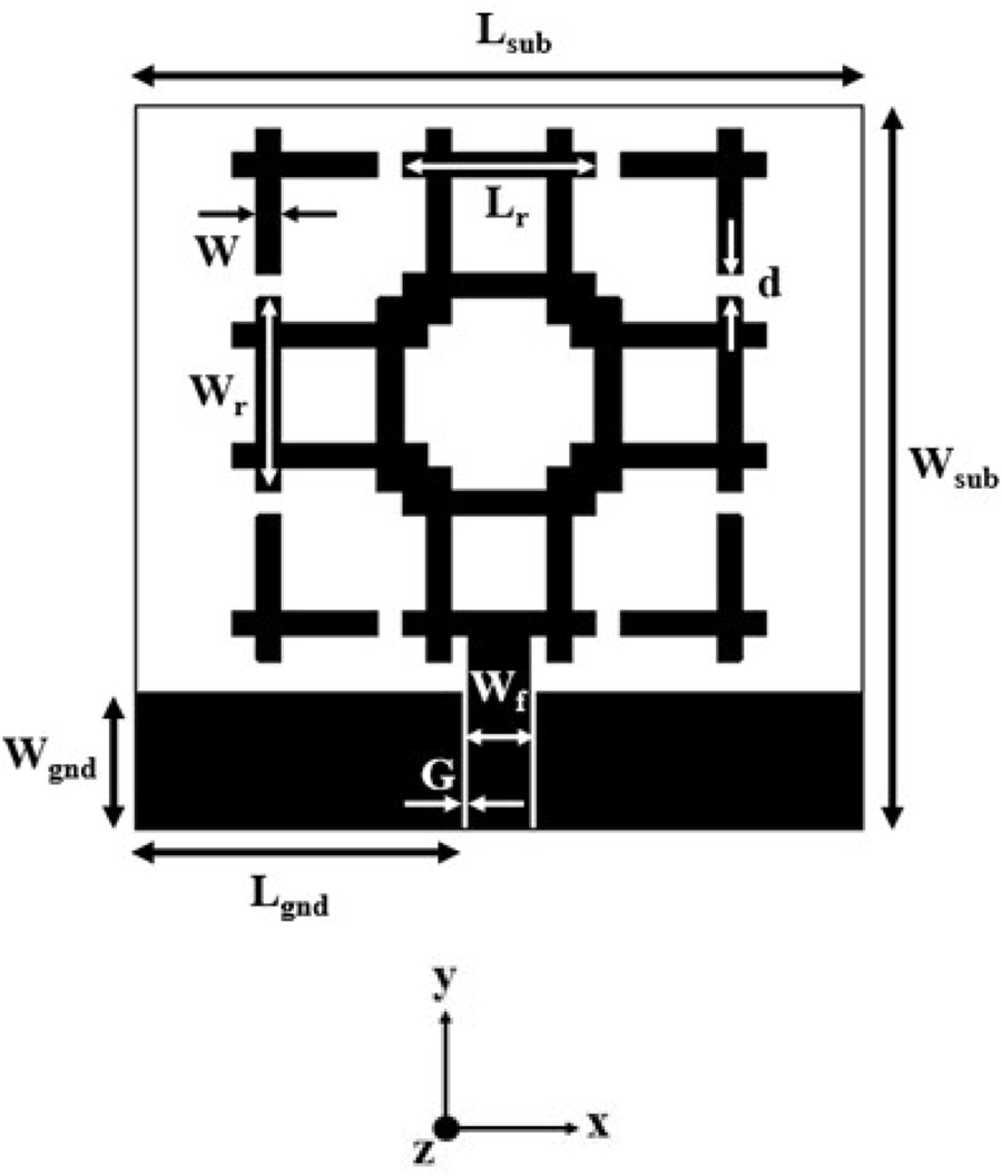
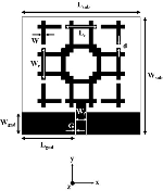
Fig. 1: Geometry of the proposed fractal antenna.
A. Antenna geometry
The design procedure of a microstrip antenna starts with selecting the proper substrate and feeding technique to achieve the required specifications. Here, in particular, the design goal is to improve the bandwidth of the antenna. To achieve wider bandwidth in our case, a CPW feed is used [17]. The feed, radiating patch, and ground plane are positioned on the same side of the substrate. FR4 with dielectric constant 4.3 is used as the substrate with a height of 1.6 mm. The dimension of the substrate is kept at 35 mm x 30 mm to accommodate the radiating patch and the ground plane. Figure 1 shows the proposed CPW-fed wideband fractal antenna. The dimensions of the same antenna are tabulated in Table 1.
Table 1: Dimensions of the proposed antenna
| Parameters | Description | Value (mm) |
|---|---|---|
| Lr | Length of the radiating square | 8 |
| Wr | Width of the radiating square | 8 |
| W | Width of rectangle strip | 1 |
| Wf | Width of CPW feedline |
2.4 |
| G | Gap of CPW line | 0.4 |
| Lsub | Length of Substrate | 30 |
| Wsub | Width of Substrate | 35 |
| Lgnd | Length of the Ground | 13.4 |
| Wgnd | Width of the Ground | 5.7 |
| -d | Gap between radiating elements |
1 |
The proposed antenna geometry consists of a T- square fractal geometry and is designed in two different stages. In the first stage, a plus-shaped radiator is generated from a conventional square patch antenna. The conventional square patch antenna is considered here as Design 1 and the antenna with a plus-shaped radiator is named Design 2. In the next stage, each square of the plus-shaped patch is replaced with a wired structure having a strip width of 1 mm and length of 8 mm for Design 3. Then following the space-filling property of fractal two L-shaped strips are added at the top corners and named Design 4. Finally, two more L-shaped strips are added to the structure at the bottom corners for the final Design 5. Two finite ground planes of the same dimensions are positioned symmetrically on both sides of the CPW feed. The dimension of the ground plane of the coplanar waveguide is 6.5 mm x 13.4 mm. The length of the feed is taken as 8 mm with a width of 2.4 mm. A gap of 0.4 mm is maintained between the coplanar ground plane and the signal strip used to feed the radiating patch. The detailed design procedure of the proposed fractal antenna along with the generator and initiator descriptions are given in the next section.
B. Design procedure
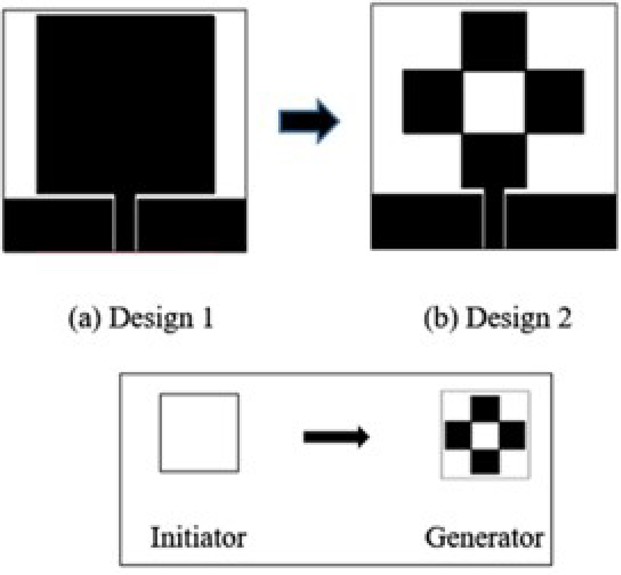
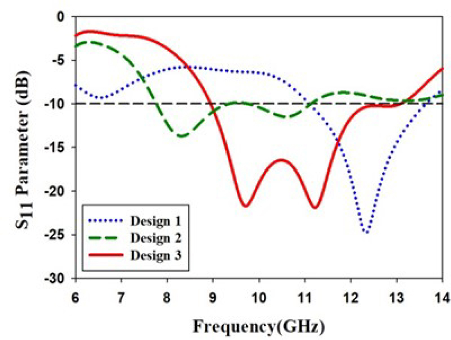
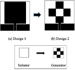
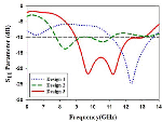
In this section, the complete design procedure for the proposed fractal antenna is described in five different design stages. In the first stage, a conventional square-shaped radiator is designed with dimensions of 22 mm x 22 mm, as shown in Fig. 2 (a). This square-shaped patch antenna is designated as Design 1 and yields a simulated bandwidth of 2.7 GHz from 11 GHz to 13.7 GHz. In the next stage, Design 2 is generated from Design 1 by replacing the initiator with the generator structure as shown in Fig. 2. Here, the square patch is considered as the initiator whereas, four square slots in the four corners with a center square slot is etched out as the Type-I generator structure for Design 2. This modified antenna gives a wider bandwidth from 7.8 GHz to 11 GHz compared to Design 1. The simulated S vs. frequency graph is plotted in Fig. 4.
Fig. 2: Construction of Design 2 from Design 1 with initiator and generator structure.
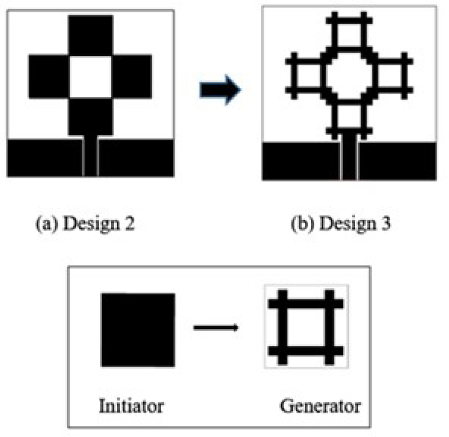
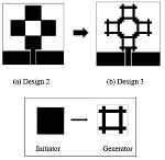
From Fig. 4, it can be seen that the s curve of Design 2 is not perfectly matched. The resonating frequency is shifted towards the left due to the increase in the current path length. Hence, to improve the impedance matching, a ‘T’ square fractal is introduced in Design 3 as the third stage. Again, in Design 3 all the square shapes of the plus-shaped initiator are replaced with a Type-II generator structure as shown in Fig. 3. The Type-II generator structure consists of four rectangular strips with a width of 1 mm and a length of 8 mm.
Fig. 3: Construction of Design 3 from Design 2 with initiator and generator structure.
The scaling dimension relation is used here to determine the dimension of the fractal design. The first iteration of the fractal is three times wide and three times taller than the generator. So, it is said to be scaled by a factor of 3. To construct iteration 1, four copies of the original generator are required. Design 3 is formed by combining four copies of the generator.
Fig. 4: S vs. frequency graphs of Design 1, 2, and 3.
Using scaling dimension relation [18],
The dimension of the above-designed fractal antenna is 1.26. After introducing the ‘T’ square fractal in Design 3, the antenna resonates from 9 GHz to 12 GHz. The s value has also improved up to 21 dB which can also be observed from Fig. 4. In Design 2, the two resonances are wide apart but in Design 3 both the resonances came closer to behaving as a single wide band. The Fractals with self-similar properties help in achieving this wider bandwidth in Design 3.
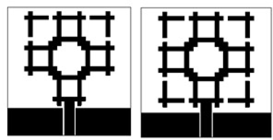
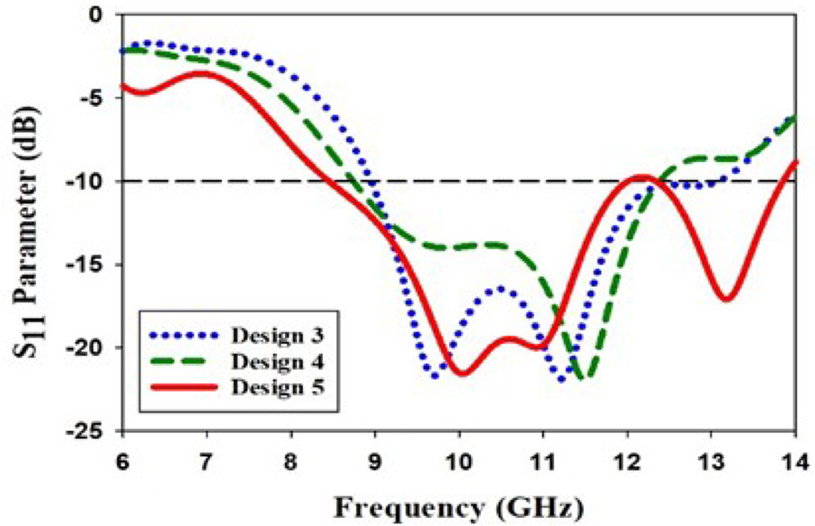
Although we have achieved a wider bandwidth of 3 GHz in Design 3, to improve the impedance bandwidth further, two L-shaped elements are introduced in the fourth stage at the top corners in Design 4 as shown in Fig. 5 (a). These L-shaped elements maintain a coupling gap with the radiator which results in improved impedance bandwidth. The coupling gap gives the capacitive effect and the inductive effect is compensated by this capacitive effect to get a wideband impedance matching characteristic from 8.7 GHz to 12 GHz in Design 4. The bandwidth of this antenna can be improved further if the antenna utilizes efficiently the available area, with its geometrical configuration. This is known as the space-filling property of fractal. Hence, to satisfy this property of fractal, in the last stage, two more L-shaped elements are added at the bottom corners of the radiator in Design 5 which is shown in Fig. 5 (b). This further increases the bandwidth from 8.4 GHz to 14 GHz. However, the s curve degrades and touches the 10 dB line at 12 GHz. The comparison among S curves of Design 3, 4, and 5 is shown in Fig. 6 over the wide range of frequency. To get a perfect impedance matching in Design 5, the parametric optimization method is adopted. Detailed procedure of the parametric optimization and its results are discussed in the coming section.
Fig. 5: (a) Design 4, (b) Design 5.
Fig. 6: S vs. frequency graphs for Design 3, 4, and 5.
C. Parametric analysis
A parametric analysis method is adopted here, for the optimization of the proposed antenna. At first, the sensitivity of the design parameters is examined over the resonance properties of the antenna. Then two design parameters, d and Wgnd are selected for the optimization process due to their impact on the antenna performance over other design parameters.
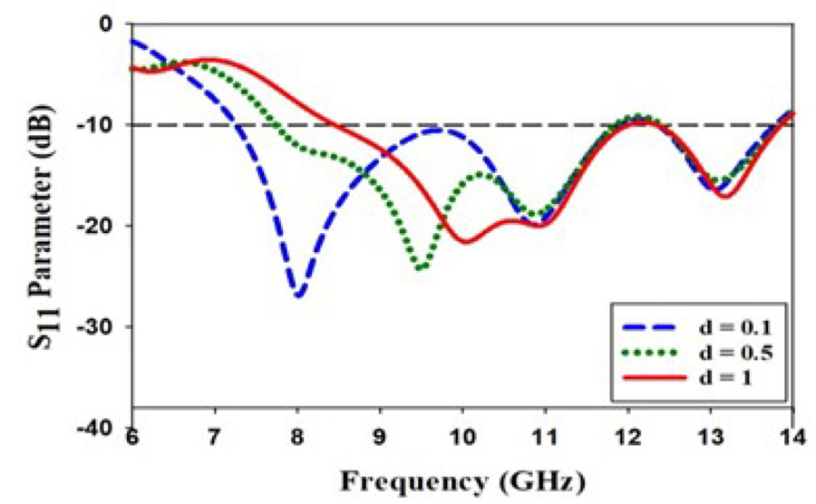
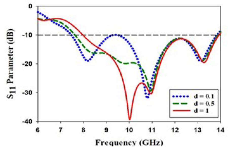
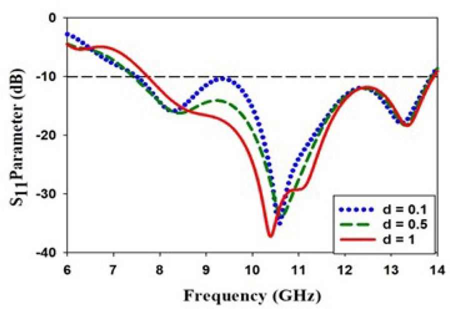
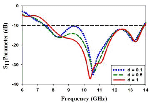
Here d is the gap between the L-shaped element and the ‘T’ square fractal and Wgnd is the width of the CPW ground. At first, the gap between the L-shaped element and the radiator, d is varied from 0.1 to 1 with a gap of 0.5 mm by keeping the width of the ground Wgnd, constant. The same process is repeated for 3 different values of Wgnd, 6.3 mm, 6 mm, and 5.7 mm.
Fig. 7: S vs. frequency graphs for the variation of ‘d’ for Wgnd = 6.3 mm.
Fig. 8: S vs. frequency graphs for the variation of ‘d’ for Wgnd = 6 mm.
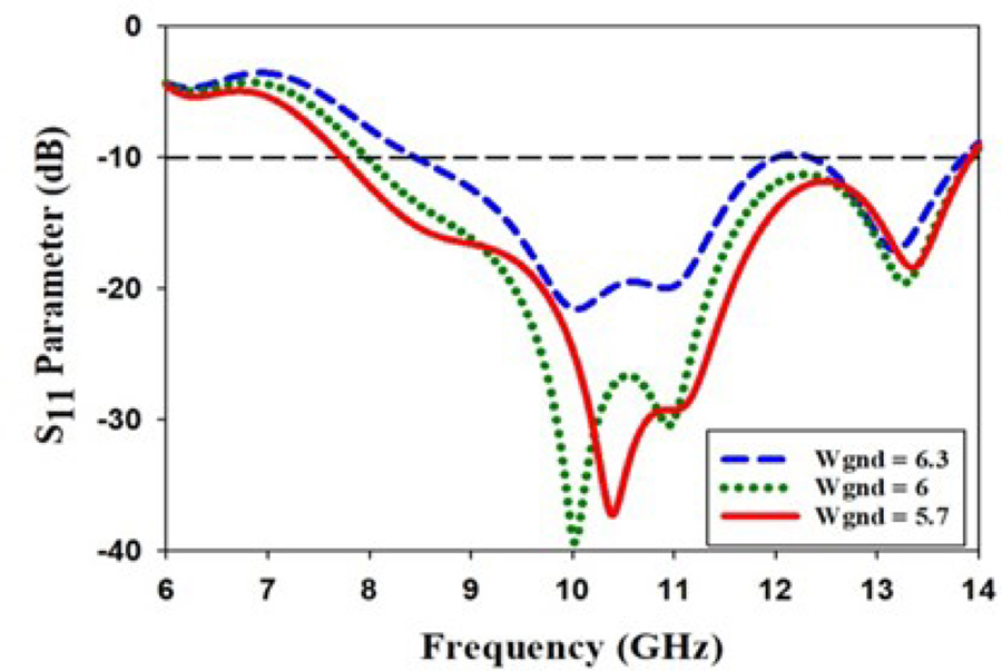
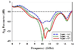
The variations of S for different values of ‘d’ are plotted in Fig. 7 for Wgnd of 6.3 mm. The same variations of S are plotted in Figs. 8 and 9, for the values of Wgnd 6 mm and 5.7 mm, respectively. It can be clearly observed from all these three figures that the bandwidth is increasing with good impedance matching when the gap d is increased from 0.1 mm to 1 mm for a constant value of Wgnd. Variation in d doesn’t have any effect on the upper resonant frequency. However, it helps in increasing the bandwidth by dropping the lower resonant frequency of the proposed fractal antenna. So, from here one can conclude that the S graph for the proposed antenna performs well for the maximum value of d i.e., 1 mm, for a constant value of Wgnd. Hence, in the next step of parametric analysis, S graphs are compared in Fig. 10 for different values of Wgnd by keeping d constant as 1 mm. The values of ground plane width Wgnd, is varied by 6.3 mm, 6 mm, and 5.7 mm for this comparison.
Fig. 9: S vs. frequency graphs for the variation of ‘d’ for Wgnd = 5.7 mm.
Fig. 10: S vs. frequency graphs for the variation of ‘Wgnd’ for d = 1 mm.
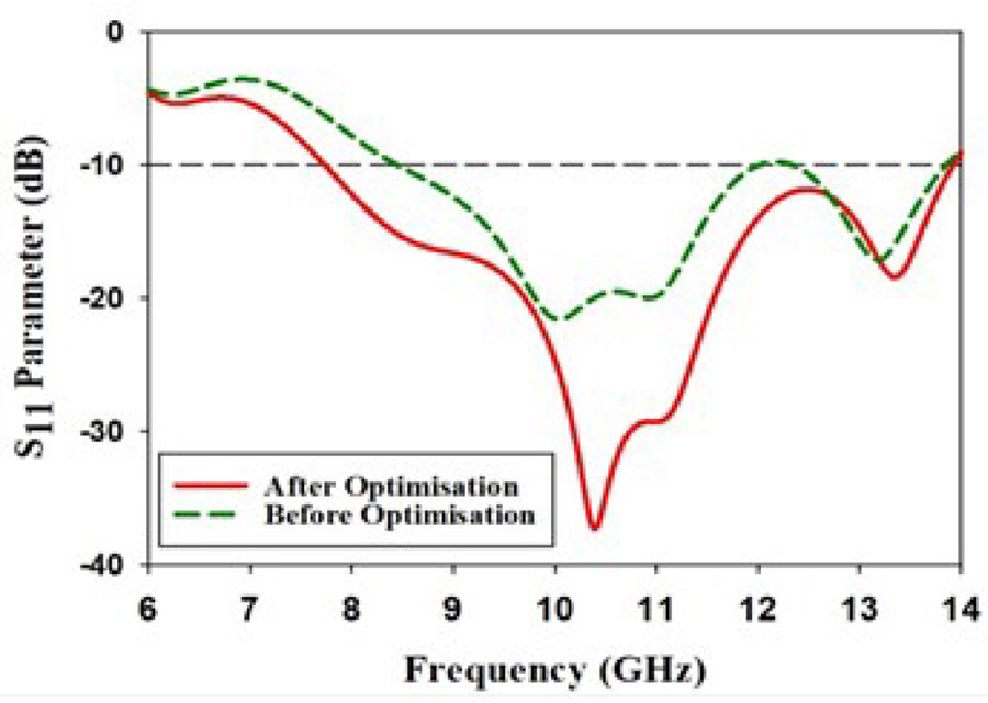
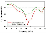
From Fig. 10, it can be seen that all the s curves are well below the 10 dB line and the impedance bandwidth is also improved compared to the last parametric analysis. The bandwidth is increasing here while decreasing the width of the ground plane from 6.3 mm to 5.7 mm. Hence, we can conclude that Wgnd = 5.7 mm and g = 1 mm gives the optimum result with a wider bandwidth from 7.7 GHz to 14 GHz and a good matching throughout this wide range of resonating frequencies. Figure 11 shows the S comparison plot for the proposed antenna before and after its optimization. An improvement in bandwidth and impedance matching can be observed in the optimized result compared to the unoptimized one.
Fig. 11: S vs. frequency graphs for the proposed design before and after optimization.
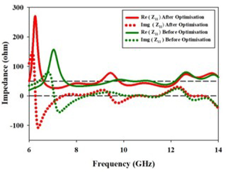
Impedance also plays a vital role in verifying the reflection characteristics and their matching for the antenna. The characteristic impedance has two components, the real part, and the imaginary part. The real part includes the resistance, whereas, the imaginary part is the reactance. To have a better insight into the reflection characteristics of the antenna, both the real and imaginary parts of the impedance are plotted in Fig. 12. It includes the impedance plots of the design before and after optimization. The simulated Z characteristics of the design in Fig. 12 elucidate that, for the whole range of the operating band, the impedance graphs are maintaining their values near the 50-ohm impedance line for the real part and 0 reactance line for the imaginary part in both before and after optimization. However, compared to the unoptimized one, a wider bandwidth is found in the design after optimizing the design parameters d and Wgnd for the antenna.
Fig. 12: Re, Img (Z) vs. frequency plot of the proposed antenna before and after optimization.
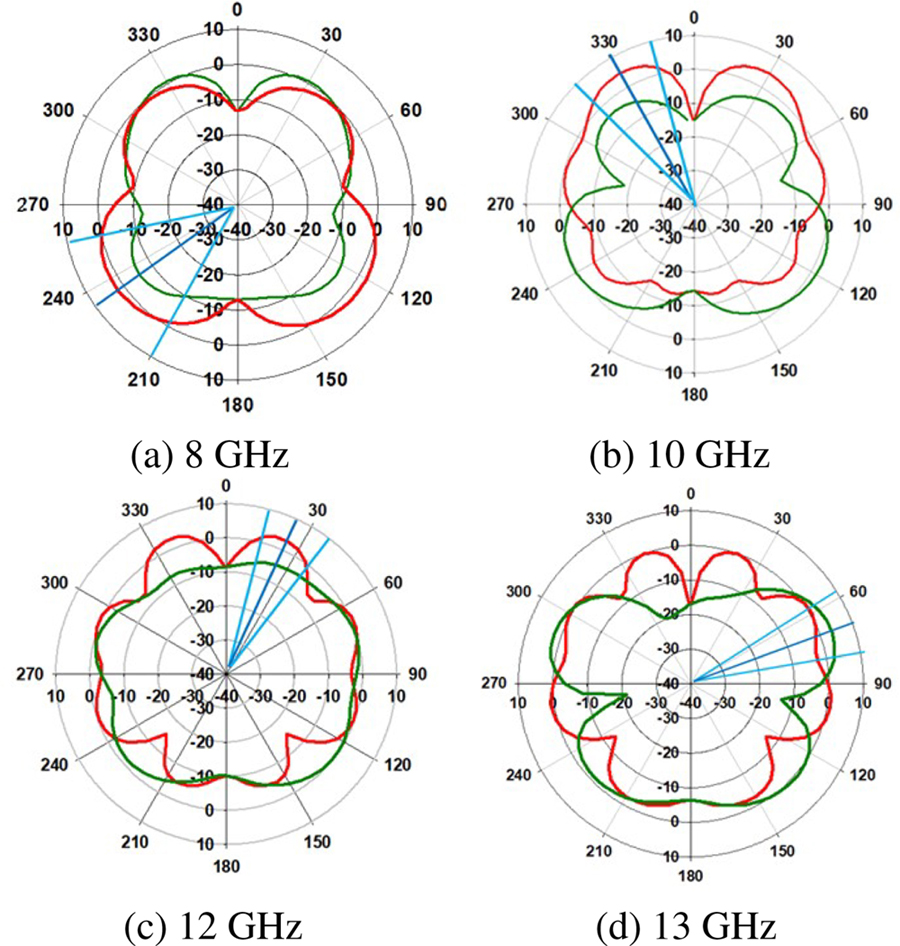
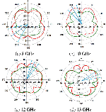
Although the proposed optimized antenna shows good reflection characteristics throughout a whole range of frequencies, the radiation patterns of the proposed wideband antenna need to be examined at different resonant frequencies. The radiation patterns for the optimized design at different frequencies are plotted in Fig. 13.
Fig. 13: Radiation pattern at (a) 8 GHz, (b) 10 GHz, (c) 12 GHz, and (d) 13 GHz without a reflector.
The XZ and YZ-plane radiation patterns are plotted at 4 different frequencies, 8 GHz, 10 GHz, 12 GHz, and 13 GHz for the optimized wideband antenna. From Fig. 13, it can be observed that the radiation patterns at all the frequencies have adequate gain values. However, from the application point of view, satellite antennas need to be unidirectional to radiate in a particular direction. But it can be seen from Fig. 13, the radiation patterns of the wideband antenna are not unidirectional. Hence, to fulfill this criterion of satellite communication, a reflector is introduced at the back of the radiator to change its radiation pattern to unidirectional. This will also improve the gain and front-to-back ratio of the proposed antenna.
III. ANTENNA WITH REFLECTOR
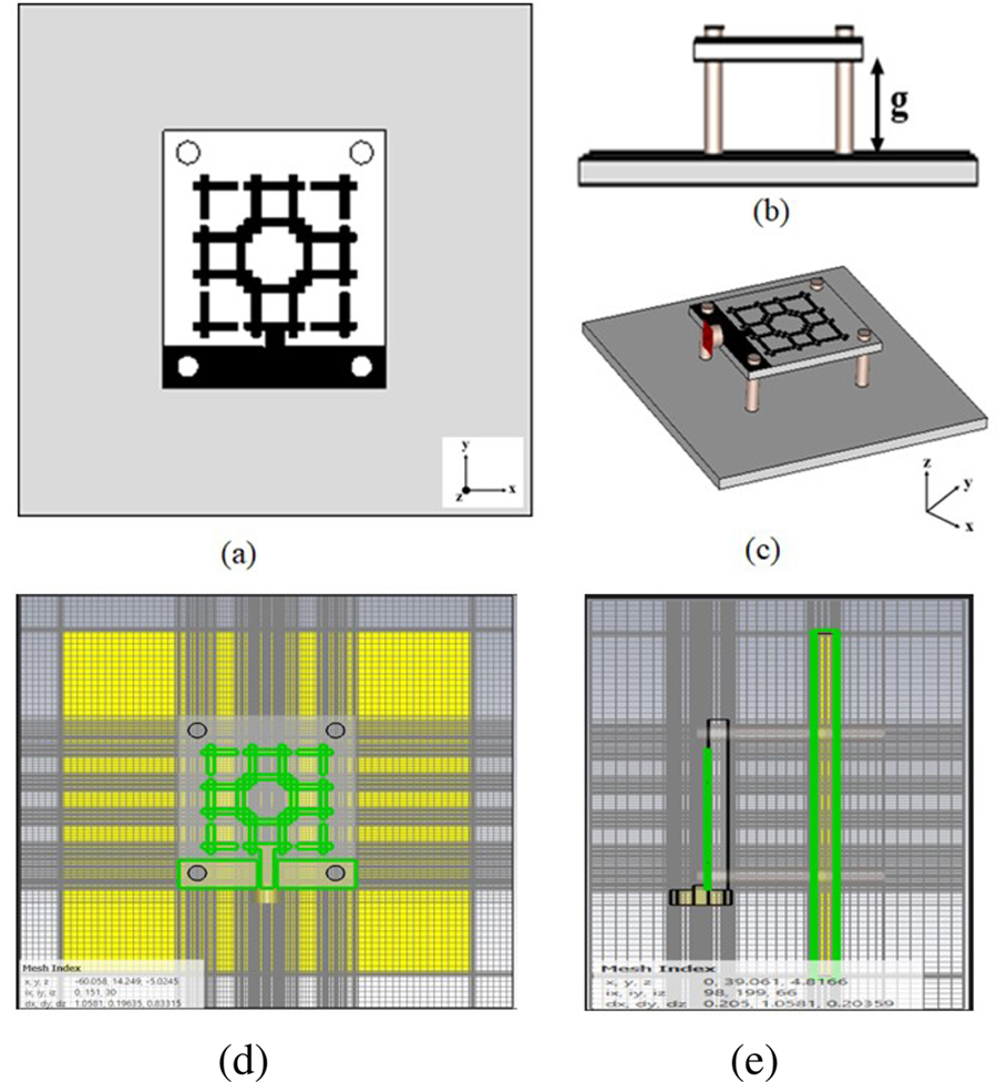
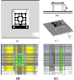
The antenna proposed here is designed with the help of the time domain (transient) solver of CST Microwave Studio. This solver makes use of Finite Integration Technique (FIT) as a computational method to solve extremely large, complex, and detailed simulations. It uses a hexahedral mesh type to analyze the designed antenna. Method on-demand approach of CST to allocate suitable solver and mesh to best fit the problem, make it more efficient and accurate for the design and analysis. Perfect boundary approximation further simplifies the analysis process. Adaptive mesh refinement, parallelization of time domain solver, automatic parametric studies, and inbuilt optimization methods can be availed in CST Microwave Studio to successfully design the 3D model and analyze the reflection and radiation properties of the antenna. For simplification of the design procedure, CST also allows us to define the properties of the background material. Pre-loaded structure templates, and excitation settings help us in the easy realization of the simulation. The hexahedral mesh view for the proposed antenna is shown in Fig. 14 for the reference of the reader. Figure 14 shows the top and side view of the proposed fractal antenna with a metal reflector below the substrate along with its mesh view for xy-and yz-planes. The reflector is used here below the substrate to reduce the back radiation. The distance between the antenna and the reflector plays an important role in creating a 180 phase shift in the back radiations, which ultimately produces a unidirectional pattern. To achieve this, the gap between the antenna and reflector (g) should be . Since the proposed antenna is resonating over a wideband ranging from 6.2 to 14 GHz, the center frequency of 10 GHz is considered for calculating the gap .
| (2) |
The size (length and width) of the reflector is taken as two times lambda.
For Centre frequency 10 GHz, . Hence, .
Fig. 14: (a) Top view, (b) Side view, and (c) trimetric view of the proposed fractal antenna with reflector. (d) Mesh view of the proposed antenna in xy-plane and (e) Mesh view of the proposed antenna in yz-plane.
The above-designed reflector acts as an infinite ground plane and reflects back the radiations to the frontal lobe for the whole wide range of frequencies. This results in a unidirectional pattern for the proposed antenna at all operating frequencies.
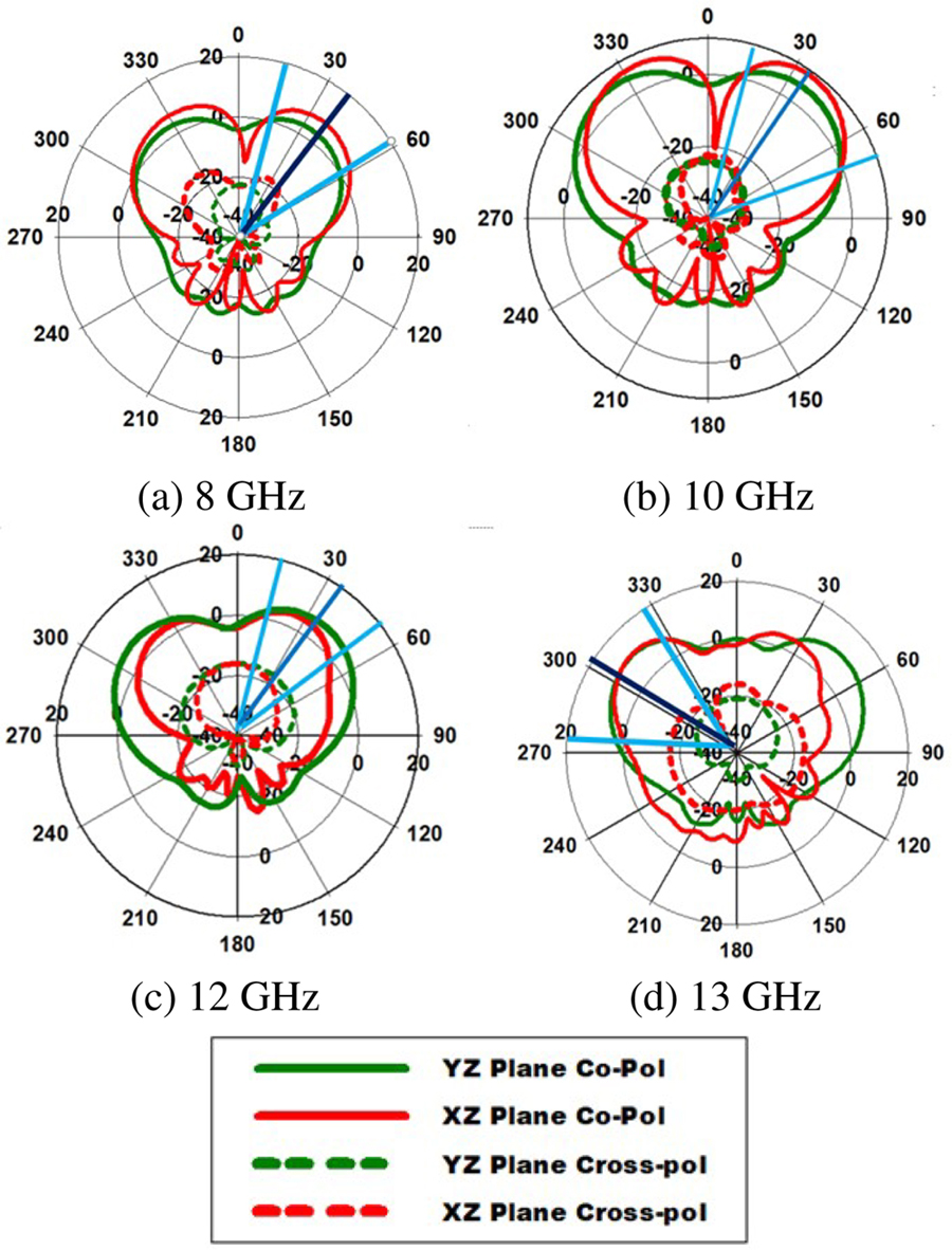
Figure 15 shows the radiation pattern for the proposed antenna after the addition of the reflector. From this figure, a clear indication can be noticed in the change in back lobes after adding the reflector at the back of the antenna. This further produces a unidirectional radiation pattern in the proposed antenna by diverting the back lobes toward the front of the radiator, which helps in increasing the overall gain of the antenna.
Fig. 15: Radiation pattern at (a) 8 GHz, (b) 10 GHz, (c) 12 GHz, and (d) 13 GHz, with reflector.
The antenna proposed here is linearly polarized. The axial ratio of the proposed antenna is found to be 40 dB, which confirms the linear polarization. Linear polarization can offer significant advantages over circular polarization. At high-frequency bands, linear polarized antennas perform well with respect to atmospheric effects such as rain attenuation. Hence, for the frequency bands where atmospheric effects are dominant and when maximum frequency re-use is needed, the advantages of linear polarization can be utilized [19]. Further, in linear polarization, co-polar side-lobe suppression and cross-polar discrimination can also be achieved in the receiving antenna.
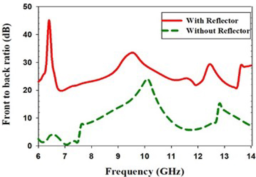
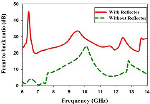
FBR has a huge impact on the directivity of the antenna. It is the ratio of the magnitude of directional radiation in a single direction divided by the radiation wasted by the antenna in other unwanted directions. Antennas with a higher front-to-back ratio can improve the signal to noise plus interference ratio efficiently which increases the overall performance of the antenna. The higher the ratio, the antenna is more directional. A directional antenna should have a front-to-back ratio of a minimum 15 dBi to accommodate itself in high-range communications [20]. Always a high front-to-back ratio is preferred as in this case less energy radiates behind the antenna in unwanted directions. The proposed antenna proves to be more efficient with a front-to-back ratio of more than 20 dB having a unidirectional pattern and a signal-to-noise plus interference ratio. As it can be seen from Fig. 16, the FBR of the antenna without a reflector is below 20 dB and when the reflector is added to the design, it increases up to 40 dB with an average FBR of 30 dB.
Fig. 16: FBR of the proposed antenna with and without a reflector.
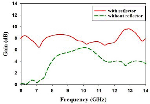
Fig. 17: Gain of the proposed antenna with and without a reflector.
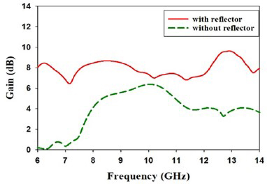
Figure 17 shows the gain of the fractal antenna with and without the reflector. The reflector helps in improving the gain of the antenna from 6.3 dBi to 10 dBi. The average gain of the antenna was found to be 3.5 dBi higher after the addition of the reflector.
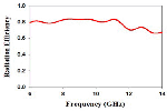
Fig. 18: Radiation efficiency of the proposed antenna.
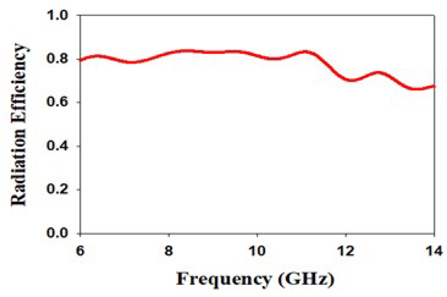
The radiation efficiency of antennas is the ratio of total power radiated by an antenna to the total input power received from the generator. In the case of an antenna with low radiation efficiency, the input power mostly dissipated because of internal losses such as metal conduction, dielectric, and magnetic losses within the antenna. Figure 18 shows the Radiation efficiency plot of the proposed antenna. The fractal antenna is radiating well with a maximum Radiation efficiency of 84% and average Radiation efficiency of 80% throughout the operating band. From CST Microwave Studio, an accepted power of 0.498 W and radiated power of 0.404 W is found for our proposed antenna at 10 GHz. Hence, the radiation efficiency is found to be 0.81 at 10 GHz for the proposed antenna. The remaining 0.094 W is dissipated in terms of Dielectric loss, metal loss, and magnetic losses.
The comparison of FBR, gain, sidelobe level, and Radiation efficiency of the antenna with and without a reflector is presented in Table 2. It is seen from the comparison table that the sidelobe level is also decreased while using a reflector.
Table 2: Comparison of antenna performance parameters with and without the reflector
| Performance Parameters |
Without Reflector |
With Reflector |
|---|---|---|
| FBR (dB) | 22 | 45 |
| GAIN (dBi) | 6.3 | 9.8 |
| SLL (dB) | 11.6 | 21.8 |
| Radiation efficiency (%) | 82 | 84 |
IV. EXPERIMENTAL RESULTS AND DISCUSSION
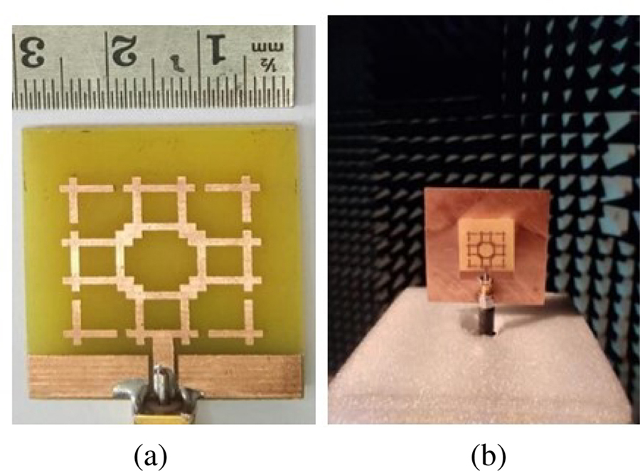
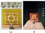
The Antenna is fabricated on an FR4 dielectric substrate with the reflector. At first, the reflection characteristics of the proposed antenna are measured in VNA. Then the radiation pattern of the fabricated antenna prototype is measured in an anechoic chamber. A horn antenna having an operating frequency range of 1-20 GHz is taken as a reference at the transmitter side, whereas the proposed T-shaped fractal antenna is placed at the receiver end as an antenna under test (AUT) for the radiation pattern measurement. A minimum distance of 2D/ is maintained to accommodate the far-field distance between the transmitter and the receiver. The radiation patterns of the fabricated antenna are measured for both XZ- and YZ-planes.
Fig. 19: (a) Fabricated antenna prototype. (b) Antenna with reflector in an anechoic chamber.
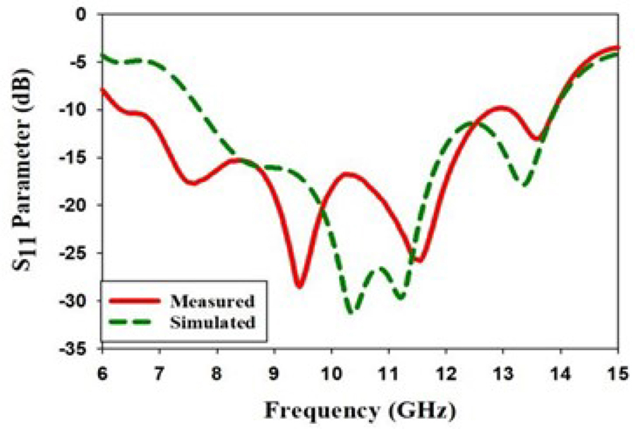
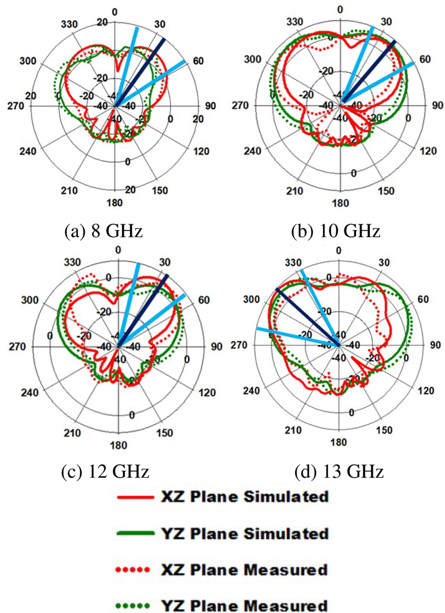
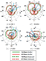
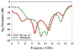
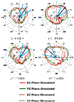
The measured results need to be verified with the simulated results. The magnitude of S parameters measured using the VNA is presented in Fig. 20. A good agreement is found between the simulated and measured results. The simulated and measured radiation patterns of the proposed antenna are plotted at 8 GHz, 10 GHz, 12 GHz, and 13 GHz frequencies for both = 0 and = 90 and shown in Figs. 21 (a), (b), (c), and (d) respectively. It can be observed from the figure, that the measured radiation patterns follow the simulated trend and a slight mismatch can be found due to minor fabrication errors.
Fig. 20: Simulated and measured S Vs. frequency for the proposed antenna.
Table 3: Comparison of antenna performance parameters with other literature
| Design | Res. Freq (GHz) | Fractional Bandwidth (%) | Dimension (mm) | Bandwidth (MHz) | Gain (dBi) |
| [7] | 11.75 | 58.7 | 60601.6 | 6900 | 6.5 |
| [13] | 6.25 | 27281.6 | 7500 | 3.35 | |
| [21] | 8.12 | 64 | 50501.6 | 5200 | 4.9 |
| [22] | 8.6 | 37.2 | 24220.25 | 3200 | 4 |
| [23] | 11 | 32 | 5050 | 3280 | 4.7 |
| [24] | 9.4 | 37.5 | 25309.8 | 3600 | 6 |
| [25] | 11 | 29 | 35354.5 | 3200 | 4.78 |
| [26] | 4.65 | 71 | 26471 | 3300 | 5 |
Antenna |
Fig. 21: Simulated and measured radiation pattern at (a) 8 GHz, (b) 10 GHz, (c) 12 GHz, and (d) 13 GHz.
A performance comparison is carried out for the proposed antenna with other antennas from various literature in Table 3. All the antennas are compared according to three important performance parameters, bandwidth, antenna gain and size of the antenna. After the application of the fractal technique, the proposed antenna exhibits a high gain of 6.3 dBi with a bandwidth of 7550 MHz. Dwivedi et al have designed an antenna in [13], having the highest fractional bandwidth of 120% than other designs. However, the same antenna has a low gain of 3.35 dBi compared to our antenna gain of 6.3 dBi. The antenna reported by Boualem et al. in [22], has a very small size but again the gain and bandwidth of this antenna are low compared to our design. After going through all the parameters of the comparison table, it is inferred that the proposed fractal antenna reported here is superior among all, in terms of its size, gain, and other performances. The proposed fractal antenna miniaturization technique is one of the simplest methods to achieve size reduction and other improved performance parameters. The antenna having such a wide band characteristic can be found suitable for a wide range of applications like earth exploration satellite, fixed satellite, radiolocation, maritime radio navigation, and aeronautical radio navigation.
V. CONCLUSION
A CPW fed ‘T’ square fractal antenna is designed for C, X, and Ku Band applications using CST Microwave Studio Software. The antenna is resonating from 6.2 GHz to 14 GHz with VSWR less than 2. Such wideband is achieved here by the use of a ‘T’ square fractal patch in combination with CPW feed. Due to the application of fractal, miniaturization is also achieved and the antenna performs well throughout the wideband with moderate gain from 6.3 to 10 dBi. A metallic reflector is incorporated in the design to make its radiation pattern unidirectional, thereby enhancing the Front-to-back ratio and the gain by minimizing backward radiations. The fractal antenna can be found suitable for many satellite applications with its balanced performance characteristics.
REFERENCES
[1] M. Kara, “The resonant frequency of rectangular microstrip antenna elements with various substrate thicknesses,” Microwave and Optical Technology Letters, vol. 11, no. 2, pp. 55-59, 1996.
[2] M. Hasan and A. Suman, “Substrate height and dielectric constant dependent performance analysis of circular microstrip patch array antennas for broadband wireless access,” American Academic and Scholarly Research Journal, vol. 4, no. 6, pp. 43-49, 2012.
[3] A. Singh and S. Singh, “Miniaturized wideband aperture coupled microstrip patch antenna by using inverted U-slot,” International Journal of Antennas and Propagation, vol. 2014, Article ID 306942, pp. 7, 2014.
[4] S. D. Targonski, R. B. Waterhouse, and D. M. Pozar, “Design of wideband aperture-stacked patch microstrip antennas,” IEEE Trans. Antennas Propag., vol. 46, pp. 1245-1251, Sep. 1998.
[5] S. H. Wi, Y. S. Lee, and J. G. Yook, “Wideband microstrip patch antenna with U-shaped parasitic elements,” IEEE Trans. Antennas Propag., vol. 55, no. 4, pp. 1196-1199, Apr. 2007.
[6] W. Liu, Z. Chen, X. Qing, J. Shi, and F. Lin, “Miniaturized wideband metasurface antennas,” IEEE Transactions on Antennas and Propagation, vol. 65 no. 12, pp. 7345-7349, 2017.
[7] T. Sarkar, A. Ghosh, l. L. K. Singh, S. Chattopadhyay and C. Sim, “DGS-integrated air-loaded wideband microstrip antenna for X- and Ku-band,” IEEE Antennas and Wireless Propagation Letters, vol. 19, no. 1, pp. 114-118, Jan. 2020.
[8] G. Varshney, V. S. Pandey, R. S. Yaduvanshi, and L. Kumar, “Wide band circularly polarized dielectric resonator antenna with stair-shaped slot excitation,” IEEE Transactions on Antennas and Propagation, vol. 65, no. 3, pp.1380-1383, Mar. 2017.
[9] B. Manimegalai, S. Raju, and V. Abhaikumar, “A multifractal cantor antenna for multiband wireless applications,” IEEE Antennas and Wireless Propagation Letters, vol. 8, pp. 359-362, 2009.
[10] G. Bharti and J. Singh, “A design of multiband nested square shaped ring fractal antenna with circular ring elements for wireless applications,” Progress in Electromagnetics Research C, vol. 108, pp. 115-125, 2021.
[11] D. V. Kiran, D. Sankaranarayanan, and B. Mukherjee, “Compact embedded dual-element rectangular dielectric resonator antenna combining sierpinski and minkowski fractals,” IEEE Transactions on Components, Packaging and Manufacturing Technology, vol. 7, no. 5, pp. 786-791, 2017.
[12] M. N. Jahromi, A. Falahati, and R. M. Edwards, “Bandwidth and impedance-matching enhancement of fractal monopole antennas using compact grounded coplanar waveguide,” IEEE Transactions on Antennas and Propagation, vol. 59, no. 7, pp. 2480-2487, Jul. 2011.
[13] R. P. Dwivedi and U. K. Kommuri, “Compact high gain UWB antenna using fractal geometry and UWB-AMC,” Microwave Optical Technology Letters, vol. 61, pp. 787-793, 2019.
[14] W. Chen, G. Wang, and C. Zhang, “Bandwidth enhancement of a microstrip-line-fed printed wide-slot antenna with a fractal-shaped slot,” IEEE Transactions on Antennas and Propagation, vol. 57, no. 7, pp. 2176-2179, Jul. 2009.
[15] Y. J. Sung, “Bandwidth enhancement of a wide slot using fractal-shaped sierpinski,” IEEE Transactions on Antennas and Propagation, vol. 59, no. 8, pp. 3076-3079, Aug. 2011.
[16] K. Vinoy and A. Pal, “Dual-frequency characteristics of Minkowski-square ring antennas,” Microwaves, Antennas & Propagation, IET, vol. 4, no. 2, pp. 219-224, Feb. 2010.
[17] R. Garg, P. Bhartia, I. J. Bahl, and A. Ittipiboon, Microstrip Antena Design Handbook, Artech House, Norwood, MA, USA, 2001.
[18] C. Balanis, Antenna Theory: Analysis and Design, Wiley, Hoboken, NJ, USA, 2005.
[19] Recommendation ITU-R BO.791, Choice of polarization for the broadcasting-satellite service.
[20] B. Wen, L. Peng, X. Li, K. Mo, X. Jiang, and S. Li, “A low-profile and wideband unidirectional antenna using bandwidth enhanced resonance-based reflector for fifth generation (5G) systems applications,” IEEE Access, vol. 7, pp. 27352-27361, 2019.
[21] S. Dhar, R. Ghatak, B. Gupta, and D. R. Poddar, “A wideband minkowski fractal dielectric resonator antenna,” IEEE Transactions on Antennas and Propagation, vol. 61, no. 6, pp. 2895-2903, Jun. 2013.
[22] B. Mekimah, T. Djerafi, A. Messai, and A. Belhedri, “Broadband circularly polarized CPW-fed asymmetrically-shaped slot patch antenna for X band applications,” Progress in Electromagnetics Research Letters, vol. 91, pp. 137-143, Jan. 2020.
[23] E. Vinodha and S. Raghavan, “A Low-profile wide band “S” shaped rectangular dielectric resonator antenna for “X” band application,” IETE Journal of Research, vol. 67, no. 4, pp. 485-490, 2021.
[24] A. Majeed, A. Abdullah, F. Elmegri, K. Sayidmarie, R. Abd-Alhameed, and J. Noras, “Dual-segment s-shaped aperture-coupled cylindrical dielectric resonator antenna for X-band applications,” IET Microwave Antennas & Propagation, vol. 9, no. 15, pp. 1673-1682, 2015.
[25] J. M. Lee, S.-J. Kim, G. Kwon, C. M. Song, Y. Yang, K.-Y. Lee, and K. C. Hwang, “Circularly polarized semi-eccentric annular dielectric resonator antenna for X-Band applications,” IEEE Antennas and Wireless Propagation Letters, vol. 14, pp. 1810-1813, 2015.
[26] A. Bhattacharya, B. Roy, S. Chowdhury, and A. Bhattacharjee, “Design and analysis of a koch snowflake fractal monopole antenna for wideband communication,” Applied Computational Electromagnetics Society (ACES) Journal, vol. 32, no. 6, pp. 548-554, 2017.
BIOGRAPHIES

Varnikha Nanthagopal received her BE from Satyabhama University in 2013, and ME from Anna University in 2016. She is pursuing a Ph.D. from Anna University, Chennai, India. Her research articles are published in many International conferences and journals. Her research interests include fractal antennas, RF, and microwave and communication.

P. Jothilakshmi completed her B.E. degree in Electronics and Communication Engineering from the University of Madras, in 1996 and her M.E. degree in Communication Systems from Madurai Kamaraj University, in 2000. She completed her Ph.D. Degree from Anna University, Chennai, India. She is serving as a lecturer from 1996 onwards. She is currently serving as a Professor in ECE at Sri Venkateswara College of Engineering, Chennai, India. She is an active fellow in professional societies ISTE, IETE, and IAENG. She led several numbers of B.E., M.E., and Ph.D.-level projects. Shehas published several SCI indexed; Scopus indexed international journal papers. She presented and published papers at international and national conferences. Her research area is Microwave antenna design and wireless communication.
ACES JOURNAL, Vol. 37, No. 9, 959–969.
doi: 10.13052/2022.ACES.J.370905
© 2022 River Publishers
