Stacked Metamaterial Patch Antenna Made of Low Permittivity Dielectrics
Bei Zhang1, Xiaofei Xu1,2,*, Xiao Deng1, Yefang Wang1, and Juzheng Wei1
1School of Communication and Information Engineering, Shanghai University, Shanghai 200444, China
2Key Laboratory of Specialty Fiber Optics and Optical Access Networks, Shanghai Institute for Advanced Communication and Data Science, Shanghai University, Shanghai 200444, China
*xfxu@shu.edu.cn
Submitted On: November 20, 2021; Accepted On: July 27, 2022
Abstract
A new concept of “meta-lo” architecture is contributed to build compact and broadband stacked metamaterial patch antennas (SMPAs). The new antennas are featured with planar mushroom metamaterials that are all made of low permittivity dielectrics. These metamaterials work as good alternatives to conventional high permittivity dielectrics, enabling the new antenna to resonate at a much lower frequency. To examine the antenna performances, one SMPA is experimentally demonstrated. The new antenna is observed to have a broad bandwidth of 27% in a volume of 0.260.260.107. The average antenna gain is 7.1 dBi in the operating bandwidth. The compact and broadband SMPA inspired by the meta-lo architecture is promising to be used in the high-speed mobile communications.
Index Terms: Broadband, compact, metamaterials, stacked patch antenna.
I. INTRODUCTION
For a long time (over 10 years), it has been deemed necessary to use material combinations of high and low (hi-lo) index dielectrics [1–3] to design a high-performance compact stacked patch antenna, which can be used in the handset high-speed communications. These stacked antennas based on the hi-lo architecture [1–3] were demonstrated with smaller parasitic and driven patches than the original stacked antennas made of a low index dielectric and air/foam [4–8]. A main limitation for these hi-lo stacked antennas is that high permittivity dielectrics are indispensable [1].
In this effort, a new “meta-lo” architecture is contributed to address the problem without utilization of any high permittivity dielectrics. In the meta-lo architecture, the lower substrate is now filled with metamaterials [9–12] as good alternatives to the high permittivity dielectrics, while the upper substrate is still a low index dielectric. It is hence named “meta-lo” after such material combinations of metamaterials and low index dielectrics. Metamaterials are composed of subwavelength functional structures that are designed included in a host natural material [9–12]. This host natural material itself might be with a low permittivity. However due to the functional inclusions, the metamaterials may exhibit an increasingly higher effective permittivity and/or permeability than the host. This idea provides a new method to make patch antennas smaller [13–20], in which only low permittivity dielectrics are utilized. Inspired by the metamaterial technology, mushroom metamaterials [20] are chosen in this contribution as the lower substrate. A particular advantage for these mushroom metamaterial structures is their planar prototype that can be well integrated into a low profile patch antenna and easily manufactured with the current printed circuit board (PCB) process.
The stacked metamaterial patch antennas (SMPAs) based on the meta-lo architecture are numerically studied in the Ansys HFSS solver. One particular SMPA is further experimentally demonstrated. It is observed to have a broad impedance bandwidth (BW) from 3.371 to 4.427 GHz (27.1%). The SMPA occupies a much smaller size than its counterpart built from a low index dielectric and air [4–8]. If we use the free space wavelength at the center frequency f (3.899 GHz) in the broad BW to measure the SMPA, we have = 76.9 mm. The parasitic patch size is 20 mm20 mm (0.260.26). The driven square patch is even smaller with side length of 0.21. The total thickness for the SMPA is 8.2 mm (0.107) in low profile. It is a particularly amazing result that such a compact SMPA is made of dielectrics all with low dielectric constant of 3. In addition, the meta-lo architecture does not sacrifice the antenna gain. The measured average antenna gain of the SMPA is 7.1 dBi in the entire BW. The radiation patterns are all observed with suppressed back lobes and cross polarizations, which benefits the directive radiation to the upper half space. We remark that a preliminarily numerical design for the SMPA was shortly reported in a conference [21]. However, new great advances are made in this work, including the introduction and discussion of new meta-lo architecture, numerical optimizations, and particularly, experimental demonstration.
II. CONCEPT OF THE META-LO ARCHITECTURE
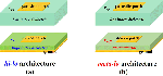
To design a compact stacked patch antenna, the traditional method is to use a hi-lo architecture [1–3], which is shown in Fig. 1 (a). It includes a parasitic patch mounted on an upper low index dielectric with dielectric constant , and a driven patch on a lower high index dielectric with . These two patches are loosely coupled to form an equivalent multi-resonant circuit and make a broad BW. Note that in the hi-lo architecture, a high permittivity dielectric is indispensable. To address the problem, an alternative meta-lo architecture is proposed in Fig. 1 (b), in which a metamaterial substrate is used to replace the high index substrate in the previous hi-lo architecture. The metamaterial substrate is made of low permittivity dielectrics, but exhibit an increased effective permittivity .
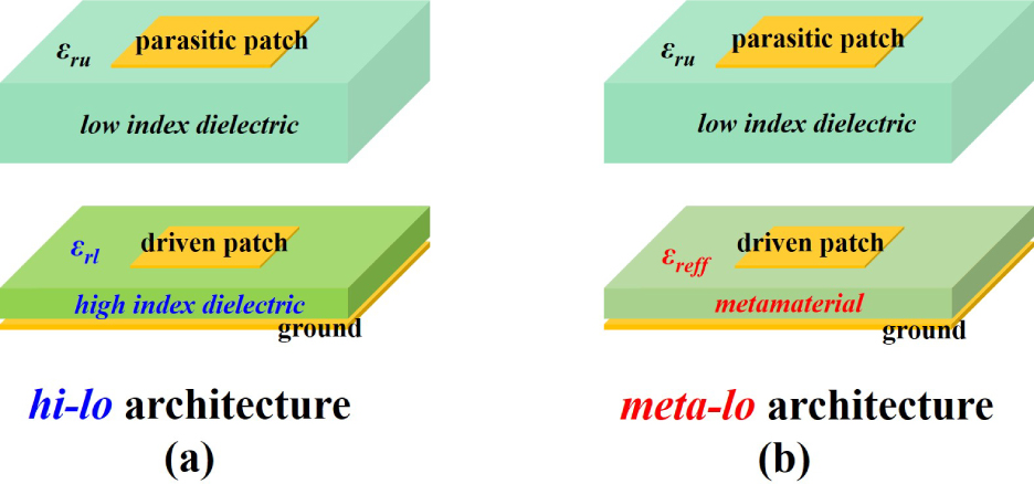
Figure 1: Comparison of (a) hi-lo architecture, and (b) meta-lo architecture to build a compact stacked patch antenna.
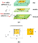
Following the meta-lo architecture, a practical SMPA is designed with planar mushroom metamaterials [20] as the effective lower substrate, while the upper substrate is still made of a natural dielectric. The metamaterial substrate is physically built from two PCB layers. As a multilayered antenna, the conceptual SMPA now includes three (top, middle, and bottom) laminate layers shown in Fig. 2 (a). The top layer works as the upper layer in the conventional hi-lo architecture. One rectangular parasitic patch with length L and width W is mounted on the top of a low index dielectric substrate with thickness h, dielectric constant , and loss tangent tan. The middle and bottom layers work together as the lower metamaterial substrate. For the middle layer, a driven patch is adhering to another dielectric with h, , and tan. It has a different patch size of LW. The bottom layer is however more complex. As shown in Fig. 2 (b), it is embedded with numerous composite mushroom structures. These composite structures are periodically distributed beneath the drive patch. The period is p along the x axis, and p along the y axis. The total number of these structures is mn (L=mp and W =np). Each mushroom element consists of a rectangular metallic “cap” mounted on the bottom dielectric, and a cylindrical conducting via perforated in the bottom substrate. The cap is connected to the ground plane by via. The mushroom cap is supposed with size of aa. And the perforated via is with an outer radius of r. The ground plane is a square with side length of G. The bottom dielectric is with h, , and tan. All of the metal layers are very thin with a small thickness of t. And all of the substrate layers are made of low permittivity dielectrics.
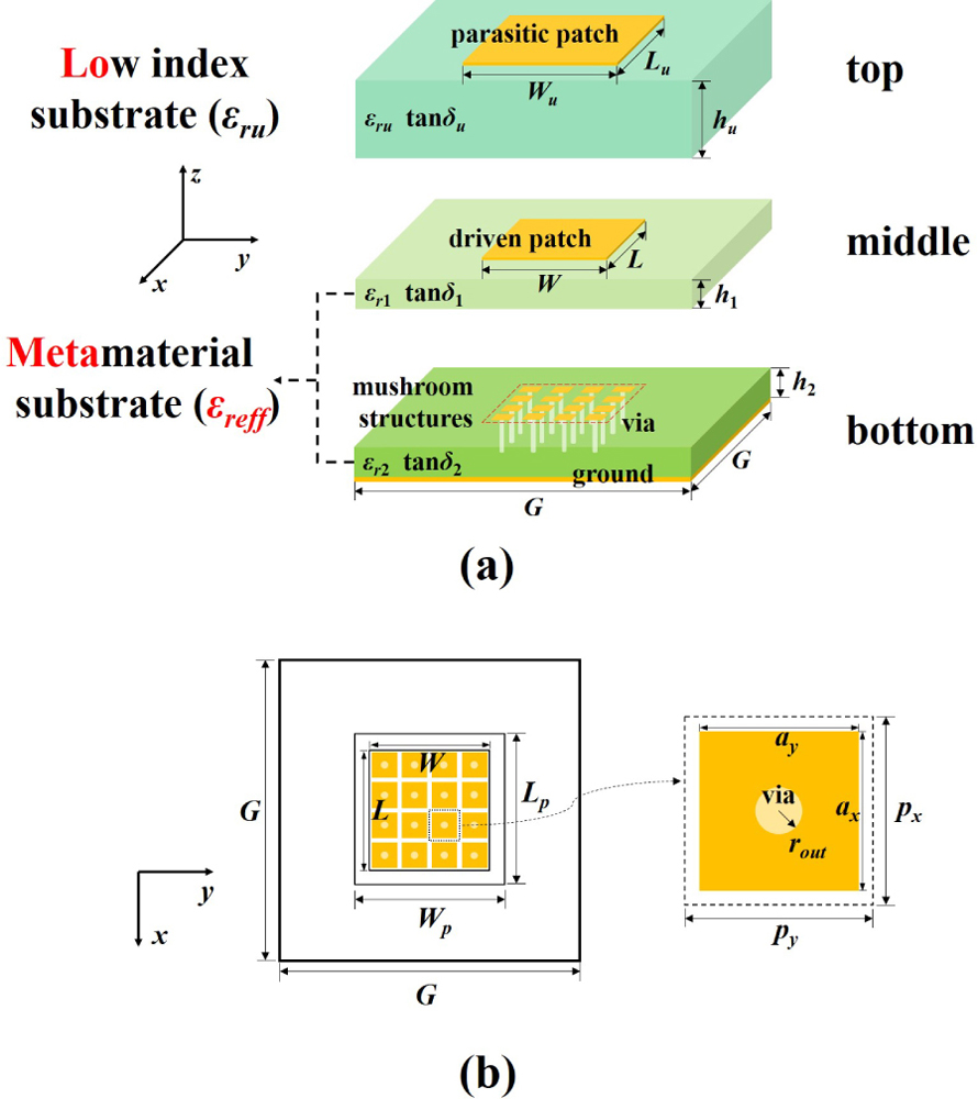
Figure 2: The configuration of the conceptual SMPA in the (a) overview, and (b) top view.
The SMPA in Fig. 2 can be viewed from two perspectives. The first perspective is that the SMPA is physically made of three layers of low permittivity dielectrics with , , and , respectively. And the second view is from the equivalent metamaterial perspective. The SMPA is built up from one low permittivity dielectric (equivalent to the top layer) with , and another metamaterial substrate (equivalent to the middle and bottom layers) with , following the meta-lo architecture.
We now discuss the of the metamaterial substrate. As seen in Fig. 2, the metamaterial substrate is loaded with periodic mushroom structures in the middle and bottom layers. These composite structures can be well treated as homogenous metamaterials on condition that p and p are much smaller than wavelength (generally less than 0.1). A simple formula can be used to describe the as [20]:
| (1) |
when , and .
Eqn (1) shows how to realize high effective permittivity metamaterials from natural low index dielectrics. The underlying mechanism is attributed to the enhanced capacitive effects in the metamaterial substrate than the original host dielectric [20]. The enhancing ratio is nearly (h+h)/h. This functionality of mushroom structures is quite different from the previous high impedance surface (HIS) in [22], despite of their similar configurations. Note that the HIS requires the p and p to be close to half wavelength (usually 0.3 to 0.5). The SMPA can be fed using various methods [4], e.g., a coaxial probe, or coupling from an aperture on the ground plane etc. To validate the concept, a practical probe-fed SMPA is designed in the following section. Its compact and broadband characteristics are demonstrated in both full wave simulations and experiments.
III. DESIGN AND RESULTS
One SMPA based on the meta-lo architecture is considered operating in the Sub-6GHz band for the broadband 5G communications. The parameters are initialized by designing a narrowband metamaterial antenna [20], which is relatively simple. The middle and bottom layers are made of SCGA-500 GF300 by Shengyi Technology Co., Ltd. (SYTECH) with = = 3, and tan = tan= 0.0023. Their thickness values are h = h = 1.52 mm. The driven patch is a square with L = W = 16 mm. The ground length is G = 50 mm. The mushroom structures are with p = p = 4 mm, a = a = 3.4 mm, and r = 0.4 mm. Using the L and in eqn (1), this narrowband antenna is predicted to resonate at nearly 3.83 GHz.
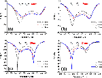
Next, we attempt to broaden the BW by adding a parasitic patch fabricated on an additional top substrate. The top substrate is chosen to be F4BM220 provided by Taizhou Wangling insulating materials factory, with = 2.2 and tan = 0.001. Its thickness is h = 5 mm, inspired by the recommended ratio of h over (h+h) in [23]. After that, we will design the parasitic patch. The parasitic patch is still a square but with length slightly larger than the driven patch. Four typical parasitic patch sizes are chosen as L = W = 18, 19, 20 and 21 mm. In addition, all of the metal layers are made of copper with thickness t = 0.035 mm. The antenna is fed by a 50 coaxial probe between the drive patch and ground plane [4, 23]. The SMPAs are numerically studied in the HFSS solver based on the finite-element method. The full-wave simulated reflection coefficients (S11s) for the cases of L = W = 18, 19, 20, and 21 mm are shown in Figs. 3 (a)–(d), respectively, which are optimized by tuning the feeding position x. The x is measured from the center of driven patch to the probe position, in the range from0 to L/2.
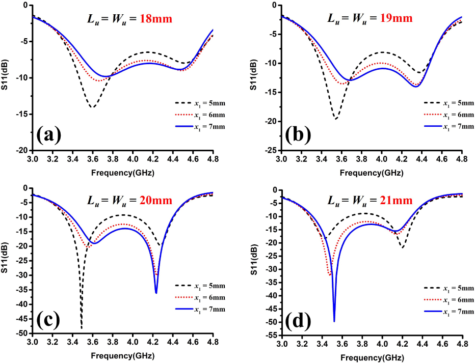
Figure 3: The full-wave calculated S11s for the SMPAs with L = W = (a) 18 mm, (b) 19 mm, (c) 20 mm, and (d) 21 mm, optimized by tuning the feeding position x.
Table 1: Simulated BW for some stacked antennas
| L = W (mm) |
x(mm) | -10 dB BW | Protuberance point |
|---|---|---|---|
| 19 | 7 | 3.52–4.46 GHz 23.6% |
-10.9 dB |
| 20 | 6 | 3.36–4.4 GHz 26.8% |
-12.4 dB |
| 20 | 7 | 3.394–4.4 GHz 25.8% |
-13.9 dB |
| 21 | 6 | 3.28–4.28 GHz 26.5% |
-11.9 dB |
| 21 | 7 | 3.32–4.28 GHz 25.3% |
-12.9 dB |
It is observed in Fig. 3 that the all of these SMPAs have dual resonant frequencies, originated from the couplings between the parasitic and driven patches [1–8]. It makes it possible to broaden the BW. However the “protuberance point” (the locally highest point between the dual resonant frequencies in the S11 curve) levels for some antennas are higher than 10 dB. Therefore, they cannot be regarded as broadband antennas, but work as “dual-band” antennas. By removing these dual-band antennas away, we finally have five potential broadband SMPAs in Table 1. Their 10 dB BWs are all very close at the order of 25%. In theory, all of these five antennas can work. However, the “protuberance point” levels are different. Considering the practical S11 may get worse than prediction, we conservatively choose the case of L = W = 20 mm and x = 7 mm, since it is with the lowest “protuberance point” of nearly 13.9 dB.
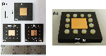
A particular SMPA is further fabricated following the optimal parameters. The SMPA in the experimental demonstration is assembled from three laminate layers. They are independently fabricated and then manually assembled together. The three different layers are shown in Fig. 4 (a). We remark that in addition to the fabrication precision (e.g., the patch size, radius of vias, dielectric constant of materials, etc.), the accuracy in the assembling work will influence the antenna performances as well. Hence one needs to be very careful when assembling the antenna. To install the coaxial probe, the middle and bottom layers should be tightly compressed with nylon screws, in order to remove the potential air layer between the dielectrics. To allow the inner pin of the feeding probe to pass through the substrates without contacting mushroom caps, some mushroom structures are deliberately designed defected around the feeding point, as shown in Fig. 4 (a). After fixing the probe, the nylon screws which were used before to attach the middle and bottom layers, are temporarily detached. The top thick substrate layer is now added and made together with the lower two layers, still with the help of nylon screws. Fig. 4 (b) shows the finally assembled SMPA.
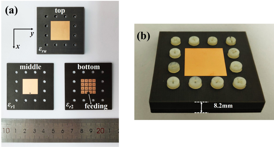
Figure 4: Photograph of (a) the three different layers, and (b) the assembled SMPA.
The SMPA in the demonstration is made by manually compacting laminate layers. It requires the laminates to be with flat surfaces, even after the PCB fabrication. Therefore, it is not recommended to use those “soft” materials (such as pure Teflon etc.) as the candidate laminates since they are very likely to be wrapped, which is harmful to the antenna assembling. A better fabrication method is to use a multilayer PCB process, without the need of trivially packaging the laminate layers by hand.
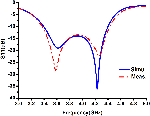
The simulated and measured S11s of the SMPA are shown in Fig. 5. Results are in good agreement. It seems to resonate at dual frequencies of about 3.6 GHz and 4.25 GHz. The simulated BW is 1.006 GHz (25.8%) from 3.394 to 4.4 GHz, while the measured result is slightly wider as 1.056 GHz (27.1%), from 3.371 to 4.427 GHz. The “protuberance point” is 13.9 dB in simulation and deteriorates to 13.5 dB in measurement, both at near 3.9 GHz. Note that the measured “protuberance point” is 3.5 dB lower than the 10 dB line, it is a relatively conservative level. In order to further broaden the BW, the “protuberance point” can be designed higher near the 10 dB line, as shown in some casesin Table 1.
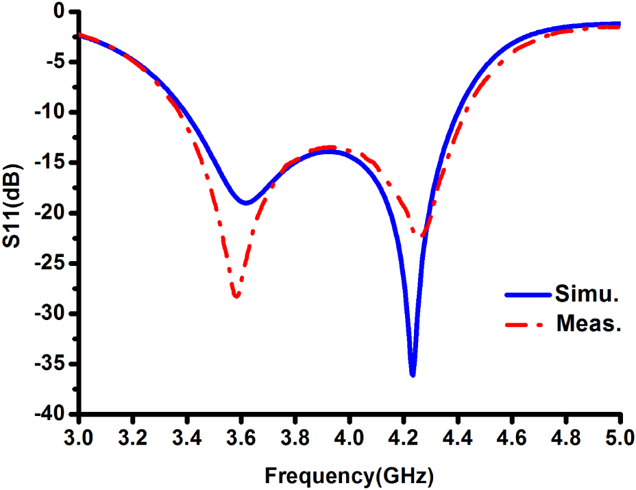
Figure 5: The simulated and measured S11s of the SMPA.
In Fig. 5, the measured f in the BW is 3.899 GHz that corresponds to = 76.9 mm. By normalizing the antenna size to , the driven patch is featured with an electrically small area of 0.210.21. The parasitic patch is larger that is 0.260.26. The total thickness of the SMPA is 8.2 mm or electrically 0.107, including all dielectric and metal layers. After these estimations, we conclude that the SMPA in the demonstration occupies a volume of 0.260.260.107, which is much more compact than the air-filled stacked patch antennas [7, 8] with a patch length of nearly 0.5 or longer.
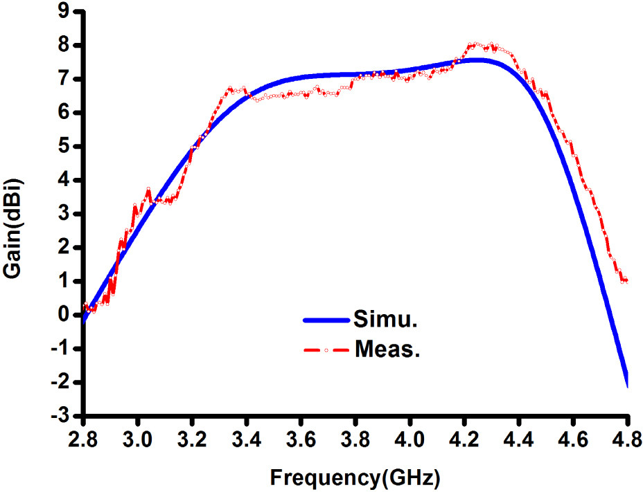
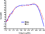
Figure 6: The antenna gain.
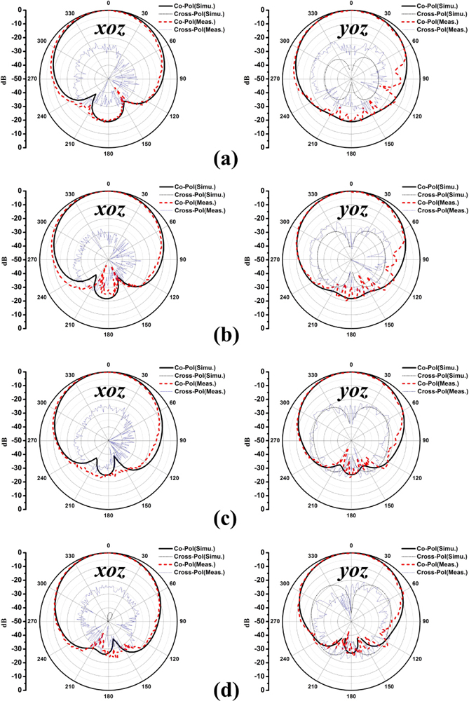
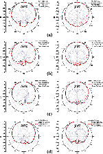
Figure 7: The radiation patterns at (a) 3.44 GHz, (b) 3.72 GHz, (c) 4.04 GHz, and (d) 4.32 GHz.
The broadband characteristics of the conceptual SMPA are also studied by measuring the antenna gain using a gain-comparison method [24]. Results are given in Fig. 6. The antenna gain curve, either from simulation or measurement, is seen very flat around 7 dBi in the operating BW. However, it descends dramatically when frequencies are out of band, resulted from the reflection loss. The simulated peak gain predicted from HFSS is about 7.6 dBi occurring at near 4.25 GHz and above 6.4 dBi in the entire BW. The measured gain curve seems less smooth. The peak antenna gain is about 8.1 dBi, still at near 4.25 GHz. In the BW, the measured antenna gain is all over 6.35 dBi. To better evaluate the broadband characteristics, a more significant statistical phrase “average gain” is used which is defined by algebraically averaging all gain values in the BW. The simulated average gain for the SMPA is about 7.2 dBi, in agreement with the measured 7.1 dBi.
The radiation patterns of the SMPA are numerically calculated and measured at four typical frequencies (3.44, 3.72, 4.04, and 4.32 GHz) so as to cover the BW as possible. Results are given in Figs. 7 (a)–(d) respectively. For each frequency, the left patterns are obtained on the xoy plane (E plane) and the right ones are on the yoz plane (H plane). The simulated co-polarized radiation patterns are quite similar with the measured ones. The back lobes are much lower than the main lobes at the broadside. An interesting trend is seen that the back lobe is becoming more suppressed when the frequency is higher. It is 19 dB at 3.44 GHz, and reduced to 27 dB at 4.32 GHz in the simulation.
The cross-polarizations are also revealed in Fig. 7. We first discuss the cases on the E plane. From the left column in Fig. 7, it is observed that the calculated cross-polarized fields on the E plane are at the order of or lower than 50 dB. They are too low to be seen. However, the measured cross-polarizations are about 23 dB. The difference might be due to the imperfection of the antenna sample. Another reason might be attributed to the measuring environment that the 50 dB level in simulation is actually too low to be detected in measurement. Now we look at the H plane patterns along the right column of Fig. 7. The simulated cross-polarizations on the H plane are seen much higher than the E plane. They are about 30 dB at 3.44 GHz, and increase to 18.3 dB at 4.32 GHz. The measured cross-polarizations are all at the order of 20 dB in the broadband. They are below 19.7 dB at 3.44 GHz and 17.7 dB at 4.32 GHz. The measured cross-polarization levels on the H plane are in consistence with the simulated levels, especially for high frequency cases. In brief, the cross-polarizations for the SMPA can be all controlled less than 17 dB in the broad band.
Table 2: Comparison of different stacked antennas
| Design | Small | Broad-band | High permittivity dielectrics | Ref. |
| lo-lo | No | Yes | Not need | [6–8] |
| hi-lo | Yes | Yes | Need | [1–3] |
| meta-lo | Yes | Yes | Not need | This |
The performances for three different stacked patch antenna architectures are summarized in Table 2. In the first design, both of the upper and lower dielectrics are made of low permittivity dielectrics [6–8] that this design is named as the lo-lo architecture as proposed in [1]. The upper dielectric is usually the air or foam that . The lo-lo architecture exhibits broadband characteristics but associated with large antenna patches. For the second hi-lo architecture, the antenna sizes can be made smaller. The limitation is that high permittivity dielectrics are necessary. In the third meta-lo architecture, the stacked antennas can be designed compact and simultaneously, broadband, which take advantage of all low permittivity dielectrics. The high permittivity dielectrics are not necessary in the new design.
IV. CONCLUSION
A new meta-lo architecture is proposed to design a compact and broad SMPA. The conceptual SMPA is all made of low dielectric constant materials. One particular probe-fed SMPA is experimentally demonstrated. It is shown with a broad impedance BW of 27%. The lateral patch dimension is 0.260.26. And the vertical profile is 0.107. The measured average antenna gain is about 7.1 dBi in the broad BW. These characteristics make the SMPA a promising component in applications of portable broadband communications.
ACKNOWLEDGMENT
This work is supported by the National Natural Science Foundation of China (No. 11904222) and the Natural Science Foundation of Shanghai (No. 16ZR1446100).
REFERENCES
[1] R. B. Waterhouse, “Stacked patches using high and low dielectric constant material combinations,” IEEE Trans. Antennas Propagat., vol. 47, pp. 1767-1771, 1999.
[2] M. A. Saed, “Reconfigurable broadband microstrip antenna fed by a coplanar waveguide,” Prog. Electromagn. Res., vol. 55, pp. 227-239, 2005.
[3] N. Nasimuddin and Z. N. Chen, “Wideband microstrip antennas with sandwich substrate,” IET Microw. Antennas Propag., vol. 2, pp. 538-546, 2008.
[4] R. Garg, P. Bhartia, I. Bahl, and A. Ittipiboon, Microstrip Antenna Design Handbook. Norwood, MA: Artech House, 2001.
[5] L. Shafai, “Wideband microstrip antennas,” in Antenna Engineering Handbook, J. L. Volakis, Ed. New York, NY: McGraw Hill, Ch. 16, 2007.
[6] R. Q. Lee, K. F. Lee, and J. Bobinchak, “Characteristics of a two-layer electromagnetically coupled rectangular patch antenna,” Electron. Lett., vol. 23, pp. 1070-1072, 1987.
[7] S. D. Targonski, R. B. Waterhouse, and D. M. Pozar, “Design of wideband aperture-stacked patch microstrip antennas,” IEEE Trans. Antennas Propag., vol. 46, pp. 1245-1251, 1998.
[8] M. A. Matin, B. S. Sharif, and C. C. Tsimenidis, “Probe fed stacked patch antenna for wideband applications,” IEEE Trans. Antennas Propag., vol. 55, pp. 2385-2388, 2007.
[9] J. B. Pendry, A. J. Holden, D. J. Robbins, and W. J. Stewart, “Magnetism from conductors and enhanced nonlinear phenomena,” IEEE Trans. Microw. Theory Tech., vol. 47, pp. 2075-2084, 1999.
[10] Y. Liu and X. Zhang, “Metamaterials: A new frontier of science and technology,” Chem. Soc. Rev., vol. 40, pp. 2494-2507, 2011.
[11] C. L. Holloway, E. F. Kuester, J. A. Gordon, J. O’Hara, J. Booth, and D. R. Smith, “An overview of the theory and applications of metasurfaces: The two-dimensional equivalents of metamaterials,” IEEE Antennas Propag. Mag., vol. 54, pp. 10-35, 2012.
[12] N. I. Zheludev and Y. S. Kivshar, “From metamaterials to metadevices,” Nat. Mater., vol. 11, pp. 917-924, 2012.
[13] R. C. Hansen and M. Burke, “Antenna with magneto-dielectrics,” Microw. Opt. Technol. Lett., vol. 26, pp. 75-78, 2000.
[14] J. Wang, Y. Li, Z. H. Jiang, T. Shi, M.-C. Tang, Z. Zhou, Z. N. Chen, and C.-W. Qiu, “Metantenna: When metasurface meets antenna again,” IEEE Trans. Antennas Propag., vol. 68, pp. 1332-1347, 2020.
[15] E. J. Rothwell and R. O. Ouedraogo, “Antenna miniaturization: Definitions, concepts, and a review with emphasis on metamaterials,” J. Electromag. Waves Appl., vol. 28, pp. 2089-2123, 2014.
[16] R. O. Ouedraogo, E. J. Rothwell, A. R. Diaz, K. Fuchi, and A. Temme, “Miniaturization of patch antennas using a metamaterial-inspired technique,” IEEE Trans. Antennas Propag., vol. 60, pp. 2175-2182, 2012.
[17] Y. Dong, H. Toyao, and T. Itoh, “Design and characterization of miniaturized patch antennas loadedwith complimentary split ring resonator,” IEEE Trans. Antennas Propag., vol. 60, pp. 772-785, 2012.
[18] M. Yang, Z. N. Chen, P. Y. Lau, X. M. Qing, and X. X. Yin, “Miniaturized patch antenna with grounded strips,” IEEE Trans. Antennas Propag., vol. 63, pp. 843-848, 2015.
[19] J. Zaid, M. Farahani, and T. A. Denidni, “Magneto-dielectric substrate-based microstrip antenna for RFID applications,” IET Microw. Antennas Propag., vol. 11, pp. 1389-1392, 2017.
[20] X. Xu and J. Wei, “Miniaturisation design of patch antenna using a low-profile mushroom type meta-substrate tailored with high permittivity,” IET Microw. Antennas Propag., vol. 12, pp. 1216-1221, 2018.
[21] X. Xu, X. Deng, and Y. Wang, “Compact and broadband stacked patch antenna loaded with mushroom metamaterials,” in Proc. Asia-Pacific Conf. Antennas Propag., pp. 1-2, 2020.
[22] D. Sievenpiper, L. Zhang, R. F. J. Broas, N. G. Alexopoulos, and E. Yablonovitch, “High-impedance electromagnetic surfaces with a forbidden frequency band,” IEEE Trans. Microw. Theory Tech., vol. 47, pp. 2059-2074, 1999.
[23] R. B. Waterhouse, “Design of probe-fed stacked patches,” IEEE Trans. Antennas Propagat., vol. 47, pp. 1780-1784, 1999.
[24] C. A. Balanis, Antenna Theory: Analysis and Design. Hoboken, NJ: Wiley, 2005.
BIOGRAPHIES

Bei Zhang was born in Henan, China, in 1997. She received the M. S. degree from Shanghai University, Shanghai, China, in 2022. Her research interest includes antenna miniaturization technology.

Xiaofei Xu received the B. S. degree in 2007 and the Ph. D degree in 2011, both from Nanjing University, Nanjing China. He is currently with the School of Communication and Information Engineering in Shanghai University, Shanghai, China.
Dr. Xu’s research areas include electromagnetics, antennas and microwave technology. He has authored over 50 papers published in peer-reviewed journals and conference proceedings. He also serves a number of journals and society workshops as the reviewer or organizer.

Xiao Deng was born in Jiangxi, China, in 1995. He received the M. S. degree from Shanghai University, Shanghai, China, in 2020. His research interest includes antenna miniaturization technology.

Yefang Wang was born in Yangzhou, China, in 1994. She received the M. S. degree from Shanghai University, Shanghai, China, in 2019. Her research interest includes electromagnetic metamaterials and antenna miniaturization technology.

Juzheng Wei was born in Gansu, China, in 1993. He received the M. S. degree from Shanghai University, Shanghai, China, in 2018. His research interest includes antenna miniaturization technology and electromagnetic metamaterials.
ACES JOURNAL, Vol. 37, No. 6, 743–749.
doi: 10.13052/2022.ACES.J.370610
© 2021 River Publishers