A Parasitic Hat for Microstrip Antenna Design Based on Defected Structures for Multiband Applications
Faten F. Ismail, Mostafa A. El-Aasser, and Nasr H. Gad
Physics Department, Faculty of Science
Ain Shams University, Cairo11566, Egypt
fatenfouad_p@sci.asu.edu.eg, elaasser@gmail.com, ngad@sci.asu.edu.eg
Submitted On: December 10, 2021; Accepted On: June 18, 2022
Abstract
In this article, a novel design of a quad-band parasitic hat microstrip antenna is proposed for multiband applications. The proposed antenna consists of a rectangular patch of dimensions 30 mm11 mm cut with four L-shaped slots connected with a rectangular slot in the middle of the front side of the antenna to form a parasitic hat based upon defected microstrip structure. On the other side of the antenna, a defected ground structure is integrated as five rectangular slots embedded in the ground plane with the same width but with various lengths. The suggested antenna is designed and fabricated on a substrate material with an area of 45 40 mm with a thickness of 1.52 mm to generate four frequency bands. The proposed antenna is fed by a microstrip transmission line. The simulated radiation patterns, return losses, maximum gains, and efficiencies of the antenna are carried out by using electromagnetic simulation software based on the finite element method. The measured return loss results validate that the suggested antenna can be designed to cover the frequency ranges from (3.8464 to 4.1456) GHz for sub-7GHz 5G applications, (6.7 to 7.162) GHz for ultra-wideband applications, (9.1616 to 9.5187) GHz for maritime radio-navigation positioning systems, and (11.5421 to 16.4085) GHz for radio-navigation satellite standards. The suggested antenna is based upon defected ground structure and defected microstrip structure techniques to improve the antennaperformance.
Index Terms: Defected ground structure, Defected microstrip structure, Microstrip antenna, Multiband, Parasitic hat, Slot antenna.
I. INTRODUCTION
In the last two decades, the microstrip patch antenna has been widely used in multiband applications [1, 2], because of its small and compact size, low profile, lightweight, low volume, and low cost. Different techniques have been used to increase the bandwidth of the microstrip antenna, such as the defected structures technique, which consists of two types; the first one is the defected ground structure (DGS). The second type is the defected microstrip structure (DMS). The DGS is a periodic or non-periodic cascading defect configuration embedded through the ground plane. The main structure used to create DGS is the electromagnetic band gap (EBG) [3]. The DGS is synthesized based on a single or many defects with periodic or aperiodic structures comparable to EBG. The DMS follows the DGS behavior but without any cutting inside the groundplane.
To enhance the microstrip antenna performance in multi-band applications either the DMS [4], or the DGS is used at the ground plane [5] or a combination of them [6]. In addition, other different techniques have been suggested to obtain multiband applications to enhance the bandwidth of the conventional patch antenna such as parasitic elements [7, 8]. With the increase of many different wireless communication systems, it is desirable to integrate a single wireless device to cover multiple wireless applications such as dual-band [9, 10], the triple band [11, 12], quad-band [13], and penta-band applications [14]. In reference [15], a dipole antenna and three microstrip slot antennas have been designed operating at 10 GHz in the X-band. In reference [16], a dual-slot radiating patch and a combination of L and U shape DGS were proposed to form a split ring structure and to get a tri-band DGS antenna for multiband applications resonating at (1.57, 2.47, and 0.926) GHz. In reference [17], two groups of five rectangular slots connected with each other by a small strip were etched in the ground plane acting as DGS to form a microstrip-fed printed slot antenna to generate five operating frequencies for multibandapplications.
In this article, the main aim of the work is to use a parasitic element, which is a non-radiating element to be placed in front of the radiating patch to direct the EM wave towards its direction. The design of aquad-band microstrip antenna with a parasitic hat element with a microstrip line feed for multiband applications is introduced. The designed antenna has an overall dimension of (45 40 1.52) mm. The suggested antenna consists of four L-shaped slots connected with a rectangular slot cut from a rectangular shaped patch of dimensions (30 11) mm. The first two L-shaped slots on the right side of the patch are connected with the other two L-shaped slots on the left side of the patch with a rectangular slot in the middle with a dimension (8 1) mm to form a parasitic hat element in the front side of the antenna acting as DMS. On the backside of the antenna, there is a defected ground plane structure in the shape of five rectangular slots of lengths of (6, 18, 30, 18, and 6) mm respectively. All five rectangular slots have the same width of 3 mm to enhance the bandwidth. The proposed antenna radiates with four bandwidths for (S 10 dB) and seven operating frequencies (4, 6.94, 9.39, 12, 12.93, 14, and 15.5) GHz suitable for multi-band applications to cover sub-7GHz 5G applications, ultra-wideband (UWB) applications, maritime radio-navigation positioning systems, and radio-navigation satellitestandards.
II. ANTENNA DESIGN AND ANALYSIS
A Antenna geometry
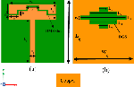
The geometry layout of the suggested parasitic hat antenna with DGS and DMS is shown in Fig. 1. The antenna uses RO4350B as a substrate material having a dielectric constant ( = 3.66), a loss tangent ( = 0.004), a dielectric thickness (h = 1.52 mm), and copper thickness (t = 0.035 mm).
As illustrated in Fig. 1, The overall area of the proposed antenna is (45 40) mm. The proposed parasitic hat antenna is composed of four L-shaped slots etched from a radiating rectangular shaped patch of a dimension (30 11) mm. Two L-shaped slots are on the right side of the patch, and the other two slots are on the left side of the patch. Four L-shaped slots are connected with a rectangular slot in the middle of a dimension (8 1) mm. The dimensions of the four L-shaped slots are the same, (6 3) mm. The parasitic hat patch antenna is located on the top of the substrate, while the DGS five rectangular slots are etched at the bottom. The width of the five rectangular slots is the same, (w=3mm) but their lengths are different; the lengths of the first, second, third, fourth, and fifth rectangular slots are (6, 18, 30, 18, and 6) mm, respectively. The proposed antenna has a linearly polarized characteristic at all operating frequencies. The proposed parasitic hat microstrip antenna is investigated by electromagnetic simulator software (high-frequency structure simulator (HFSS)) based on the finite element method (FEM) [18].
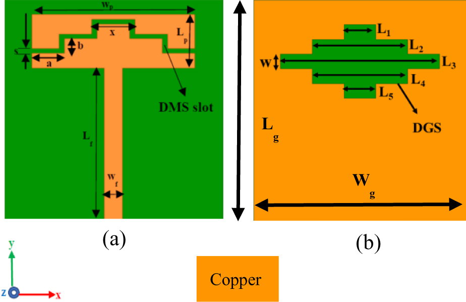
Figure 1: The geometry of the proposed parasitic hat antenna (a) front view (patch) and (b) back view (ground).
All the parameters for the suggested antenna are given in Table 1.
Table 1: Optimized parameters of the proposed parasitic hat microstrip antenna
| Para-meter | Value (mm) | Para-meter | Value (mm) | Para-meter | Value (mm) |
| W | 40 | b | 3 | L | 18 |
| L | 45 | x | 8 | L | 30 |
| h | 1.52 | L | 11 | L | 18 |
| W | 3.35 | W | 30 | L | 6 |
| L | 31 | s | 1 | w | 3 |
| a | 6 | L | 6 | - | - |
B Design procedure
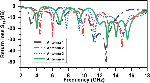
DGS and DMS have an essential role in broadening the bandwidth of the microstrip antennas. In this section, they will be employed to choose the most suitable antenna structure to obtain a multiband antenna; four design configurations were carried out. Fig. 2 shows the design procedure of the ground plane, and patch by using the four configurations. Fig. 3 shows the return loss (S) for the different configurations (from antenna 1 to antenna 4).
As illustrated in Fig. 2 (a), in the first configuration (antenna 1), five rectangular slots of the same width but having different lengths are embedded in the ground plane with a transmission line of length 36 mm. The resonance frequencies (3.2, 6.1, 11.2, 12.7, and 16.8) GHz were obtained. Fig. 2 (b), in the second configuration (antenna 2), (4.4, 6, 9.8, 11, 13.2, and 14.8) GHz resonance frequencies are obtained by adding a rectangular radiating patch of a dimension (30 11) mm in the front side of the antenna. On the other side of the antenna 2, the five rectangular slots are etched in the ground plane. The length of the rectangular patch (L) is chosen as approximately equal to half of the wavelength at the resonant frequency and can be calculated using the equations below [19]:
| (1) | ||
| (2) |
where C is the speed of light in a vacuum, is the relative permittivity, is the effective relative permittivity, L is the length of the rectangular patch, and f is the fundamental resonant frequency.
To achieve multiband operation for the proposed antenna, the lengths of DGS and DMS slots must be around g/2 for all operating frequencies (f) based on the following equation:
| (3) |
where is the guide wavelength [20].
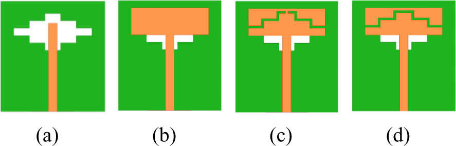
Figure 2: DGS, DMS evolution configurations (a) antenna 1, (b) antenna 2, (c) antenna 3, and (d) antenna 4.
The third configuration (antenna 3) of Fig. 2 (c) provides a wider bandwidth by employing a parasitic hat-shaped embedded in the radiating patch by etching four L-shaped slots of dimension (6 3) mm. Two rectangular slots, with the dimension (3.5 1) mm, are removed from the rectangular patch. There is an only individual rectangular strip with the dimension (1 1) mm that connects between the upper and lower parts of the radiating patch and acts as an inductively coupling. The obtained antenna provides the resonance frequencies (7.7, 9.4, 11.3, 15) GHz.
Finally, as shown in Fig. 2 (d) in the fourth configuration (antenna 4), the desired parasitic hat multiband antenna is obtained by cutting a rectangular strip of a dimension (1 1) mm that connects the upper and lower parts of the antenna to form the proposed parasitic hat antenna. It acts as a capacitively coupling to obtain seven operating frequencies (4, 6.94, 9.39, 12, 12.93, 14, and 15.5) GHz with return losses ( 21, 17, 15, 16, 40, 22, and 43) dB, respectively for multiband applications.
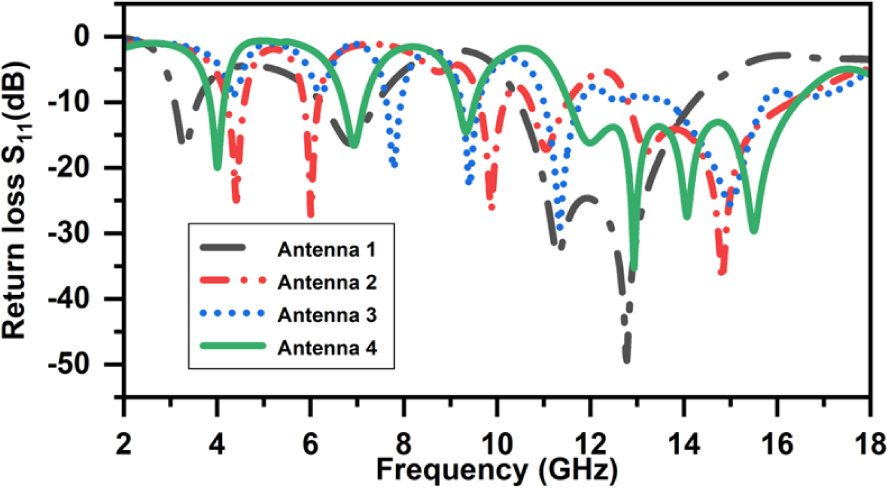
Figure 3: Simulated return loss (S) for different configurations (antenna 1 to antenna 4).
All the operating frequencies with the antenna configurations (antenna 1 to antenna 4) are given inTable 2.
Table 2: Antenna configurations (antenna 1 to antenna 4) with their operating frequencies
| Antenna configurations | Frequency (GHz) |
|---|---|
| Antenna 1 | 3.2, 6.8, 11.3, 12.7 |
| Antenna 2 | 4.4, 6, 9.8, 11, 13.2, 14.8 |
| Antenna 3 | 7.7, 9.4, 11.3, 15 |
| Antenna 4 (proposed) | 4, 6.94, 9.39, 12, 12.93, 14, 15.5 |
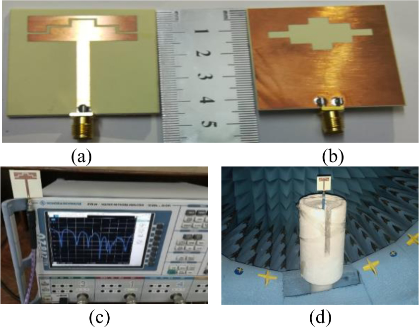
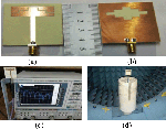
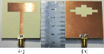
Figure 4: Fabricated proposed parasitic hat antenna (a) front side (b) backside (c) return loss S observed in VNA (d) the antenna in the Anechoic Chamber.
III. RESULTS AND DISCUSSION
A Return loss (S)
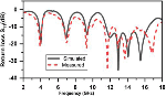
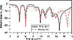
The return loss is measured with Rohde and Schwarz ZVB20 vector network analyzer (VNA), which has a frequency range limited to 20 GHz. Fig. 4 displays the fabricated antenna frontside, backside, return loss S observed in VNA, and the antenna in the Anechoic Chamber. Fig. 5 shows the simulated and measured return loss S of the proposed multiband antenna. The simulated result shows a bandwidth from (3.8 to 16.4) GHz, whereas the obtained measured bandwidth is from (3.6 to 17.4) GHz.
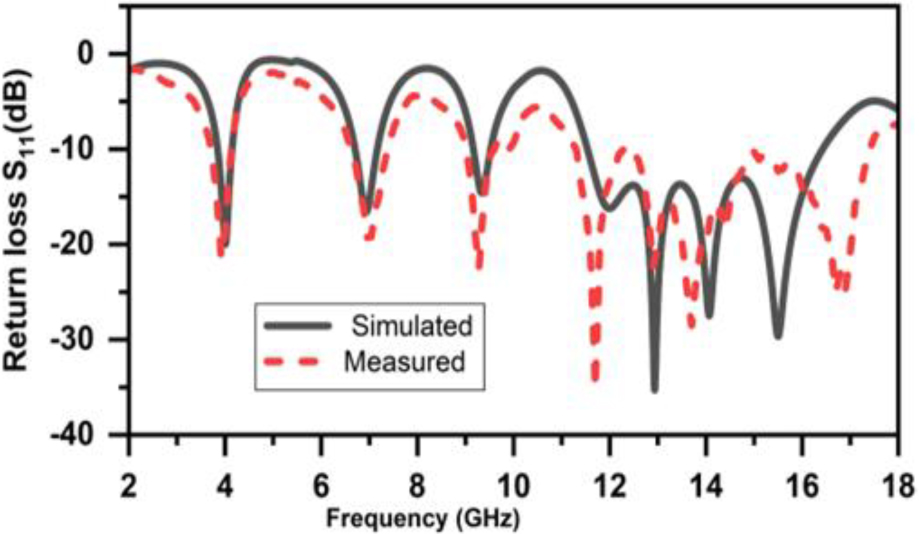
Figure 5: The simulated and measured return loss S of the proposed parasitic hat antenna.

Figure 6: Fabricated full rectangular patch antenna with DGS (a) top view(b) bottom view.
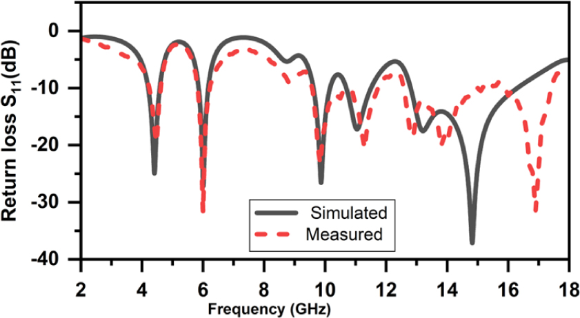
Figure 7: The simulated and measured return loss S of the rectangular patch antenna with DGS.
For verifying the full rectangular radiating patch antenna of dimension (30 11) mm with five rectangular slots as DGS is fabricated and shown in Fig. 6. The return loss results (measured and simulated) for the fabricated rectangular patch antenna are illustrated in Fig. 7.
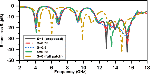
B Parametric study for the effect of parasitic spacing
In this section, a parametric study for five different values for the spacing (s) between the patch and the parasitic hat element is shown. Fig. 8 displays the simulated return loss S for different values for the spacing (s) between the patch and the parasitic hatelement.
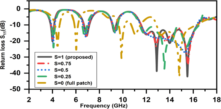
Figure 8: The return loss Sfor five different values for spacing (s) between the patch and the parasitic hat.
All five different values of the spacing (s) with the resonating frequencies and their return losses are given in Table 3.
Table 3: Five different values of the spacing (s) with their resonating frequencies, and return losses
| Spacing (s)(mm) | Resonatingfrequency (GHz) | Return loss S(dB) |
|---|---|---|
| 1(Proposed) | 4, 6.94, 9.39, 12,12.93, 14, 15.5 | 21, 17, 15,16, 40, 22, 43 |
| 0.75 | 4,6.8,9.2,12,12.8,13.6,15.5 | 19, 17, 14,15, 23, 20, 34 |
| 0.5 | 4,6.8,9.3,15.3 | 24, 18, 16,15, 37, 23 |
| 0.25 | 4,6.7,9.3,11.8,13.5, 15.4 | 24, 18, 16,15, 37, 23 |
| 0(Full patch) | 4.4,6,9.8,11,13.2,14.8 | 25, 26, 31,16, 16, 42 |
Table 3 shows that the proposed parasitic hat antenna (s = 1) is the best result.
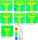
C Surface current distribution (J)
The current density distribution across the proposed antenna lattice at multiple resonant frequencies is shown in Fig. 9 (a)-(g).

Figure 9: Simulated surface current density distribution of the proposed antenna at (a) 4GHz, (b) 6.94 GHz, (c) 9.39 GHz, (d)12 GHz, (e) 12.93 GHz, (f) 14 GHz, and (g) 15.5 GHz.
D Antenna radiation patterns, gain, and efficiency
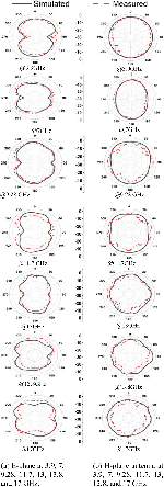
The radiation patterns of the proposed omnidirectional antenna at different bands in E-plane (Y-Z plane) and H-plane (X-Z plane) areas at different resonance frequencies are simulated, measured, and illustrated in Fig. 10.
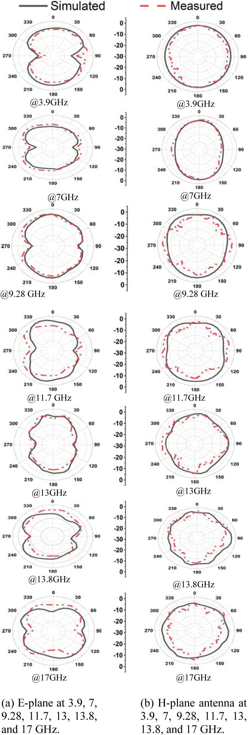
Figure 10: Simulated and measured radiation pattern (E-plane and H-plane) of the proposed antenna at (3.9, 7, 9.28, 11.7, 13, 13.8, and 17) GHz.
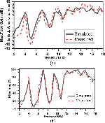
Figures 11 (a), and (b) illustrate the simulated and measured maximum gain and radiation efficiency versus frequency (freq.) for the proposed multiband antenna, respectively.
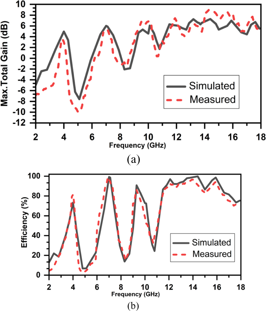
Figure 11: (a) Simulated and measured maximum gain vs frequency, and (b) Simulated and measured radiation efficiency vs frequency for the proposed antenna.
All simulated and measured values of maximum gain and efficiency of the proposed antenna are shown in Table 4.
Table 4: The simulated and measured maximum gain, and efficiency of the proposed parasitic hat antenna
| Resonant freq. (GHz) | MaximumGain (dB) | Efficiency(%) | |||
| Sim. | Meas. | Sim. | Meas. | Sim. | Meas. |
| 4 | 3.9 | 4.9 | 3.6 | 73.32 | 79.29 |
| 6.49 | 7 | 6 | 5.5 | 95.2 | 86.11 |
| 9.39 | 9.28 | 4.7 | 5.4 | 89.88 | 87.48 |
| 12 | 11.7 | 6 | 6 | 94.94 | 91.75 |
| 12.39 | 13 | 6.53 | 6 | 93.61 | 93.61 |
| 14 | 13.8 | 6.57 | 4.9 | 98.97 | 95.43 |
| 15.5 | 17 | 6 | 5.9 | 94.28 | 75.11 |
A comparison of the obtained results of the proposed antenna with recently published work is given inTable 5.
Table 5: Comparison of the proposed parasitic hat antenna with recently published work
| Ref. No. | Antenna size (mm), Material | Resonance freq. (GHz) | Techniques |
|---|---|---|---|
| [21] | 45451.6, FR4 epoxy | 5,6.8,7.5,8.5 | Parasitic element |
| [22] | 20 301.6, FR4 epoxy | 2.26,3.6,5.3 | DGS, monopole |
| [23] | 27.5201.5, FR4 epoxy | 2.44,3.55,5.6 | DMS, monopole |
| [24] | 58 480.8, FR4 epoxy | 2.2,2.3,2.5 | DGS, Parasitic |
| This work | 45 401.52, RO4350 | 4, 6.94, 9.39, 12, 12.93, 14, 15.5 | DGS, DMS, Parasitic element |
IV. CONCLUSION
In this article, a novel design of a microstrip patch antenna with a parasitic hat has been proposed for multiband applications such as sub-7GHz 5G applications, ultra-wideband (UWB) applications, maritime radio-navigation positioning systems, and radio-navigation satellite standards. The presented antenna has multiple bandwidths starting from 3.8 to 16.4 GHz with less than 10 dB return loss (S) within the region. Three methods of enhancing the performance of the rectangular microstrip patch antenna were employed. The measured operating frequencies are (3.9, 7, 9.28, 11.7, 13, 13.8, and 17) GHz with return losses (21.4, 19.2, 22.5, 35.2, 25.2, 29.1, and 26.8) dB, respectively. In conclusion, the antenna achieves stable radiation patterns, higher radiation on efficiency, and broad bandwidth around the operating frequencies 0.29 GHz with (7.48%) at 4 GHz, 0.462 GHz with (6.66 %) at 6.94 GHz, 0.3571 GHz with (3.823 %) at 9.39 GHz, 0.96 GHz with (7.99 %) at 12 GHz, 0.97GHz with (7.4 %) at 12.93GHz, 1.28GHz with (9.07 %) at 14 GHz, and 1.66 GHz with (10.66 %) at 15.5 GHz. The simulated results show that the DGS, DMS, and parasitic elements are critical factors for improving the bandwidth of the proposedantenna.
REFERENCES
[1] A. J. Khalilabadi and A. Zadehgol, “Multiband antenna for wireless applications including GSM/UMTS/LTE and 5G bands,” Applied Computational Electromagnetic Society (ACES) Journal, vol. 34, no. 2, pp. 270-271, Feb. 2019.
[2] A. Ahmad, F. Arshad, S. I. Naqvi, Y. Amin, and H. Tenhunen, “Design, fabrication, and measurements of extended l-shaped multiband antenna for wireless applications,” Applied Computational Electromagnetic Society (ACES) Journal, vol. 33, no. 4, pp. 388-393, Apr. 2018.
[3] Md. Sh. Alam, N. Misran, B. Yatim, and M. T. Islam, “Development of electromagnetic band gap structures in the perspective of microstrip antenna design,” International Journal of Antennas and Propagation, 2013.
[4] K. Hossain, T. Sabapathy, M. Jusoh, P. J. Soh, R. B. Ahmad, M. I. Jais, and Q. H. Abbasi, “A frequency-reconfigurable microstrip antenna with constant dipole-like radiation patterns using single bias, triple varactor tuning with reduced complexity,” Wireless Personal Communications, pp. 1-22, 2021.
[5] M. A. Gaber, F. F. Ismail, A. Yahia, M. A. El-Aasser, and N. H. Gad, “A printed antenna design with defected ground structure for multiband applications,” European Journal of Science and Technology, no. 28, pp. 1528-1533, Nov. 2021.
[6] F. F. Ismail, M. A. Gaber, M. A. El-Aasser, and N. H. Gad, “Design of a mirror dtairs multiband microstrip antenna using defected structures,” In 38th National Radio Science Conference (NRSC), vol. 1, pp. 47-55. IEEE, 2021.
[7] M. El-Sayed, A. Yossry, A. Yahia, M. A. El-Easser, and N. H. Gad, “Printed monopole antenna design with parasitic element for multi-band applications,” In 2021 International Conference on Electronic Engineering (ICEEM), pp. 1-4. IEEE, 2021.
[8] Y. Deng, X. F. Li, and J. S. Hong, “A compact tri-band miniaturized antenna with parasitic elements loading,” Applied Computational Electromagnetic Society (ACES) Journal, vol. 35, no. 7, pp. 829-836, Jul. 2020.
[9] O. Amjad, S. W. Munir, S. T. Imeci, and A. O. Ercan, “Design and implementation of dual band microstrip patch antenna for WLAN energy harvesting system,” Applied Computational Electromagnetic Society (ACES) Journal, vol. 33, no. 7, pp. 746-751, Jul. 2018.
[10] A. E. Farahat and K. F. A. Hussein, “Dualband (28/38 GHz) MIMO antenna system for 5G mobile communications with efficient DoA estimation algorithm in noisy channels,” Applied Computational Electromagnetics Society (ACES) Journal, vol. 36, no. 3, Mar. 2021.
[11] K. Fertas, H.Kimouche, M. Challal, H.Aksas, R. Aksas, and A. Azrar “ Design and optimization of a CPW-Fed tri-band patch antenna using genetic algorithms,” Applied Computational Electromagnetic Society (ACES) Journal, vol. 30, no. 7, Jul. 2015.
[12] M. H. B. Ucar and Y. E. Erdemli, “Triple-band microstrip line-fed printed wide-slot antenna for WiMAX/WLAN operations,” Applied Computational Electromagnetic Society (ACES) Journal, vol. 29, no. 10, pp. 793-800, Oct. 2014.
[13] E. W. Coetzee, J. W. Odendaal, and J. Joubert, “A quad-band antenna with AMC reflector for WLAN and WiMAX applications,” Applied Computational Electromagnetic Society (ACES) Journal, vol. 33, no. 10, pp. 1123-1128, Oct. 2018.
[14] C. H. Chang and K. L. Wong, “Printed /8-PIFA for penta-band WWAN operation in the mobile phone,” IEEE Trans. Antennas Propag., vol. 57, no. 5, pp. 1373-1381, May 2009.
[15] A. A. Eldek, A. Z. Elsherbeni, C. E. Smith, and K. Lee, “Wideband planar slot antennas,” Applied Computational Electromagnetic Society (ACES) Journal, vol. 9, no. 1, 2004.
[16] R. Patel, A. Desai, and T. K. Upadhyaya, “An electrically small antenna using defected ground structure for RFID, GPS and IEEE 802.11 a/b/g/s applications,” Progress In Electromagnetics Research Letters, vol. 75, pp. 75-81, 2018.
[17] N. H. Gad and M. Vidmar, “Design of a microstrip fed printed-slot antenna using defected ground structures for multiband applications,” Applied Computational Electromagnetic Society (ACES) Journal, vol. 33, no. 8, pp. 854-860, Aug. 2018.
[18] ANSYS® Electromagnetics Student, ver. 2.2.1. Online: Ansys | Engineering Simulation Software.
[19] C. A. Balanis, Antenna Theory: Analysis and Design. John Wiley & Sons, 2016.
[20] R. Garg, P. Bhartia, I. Bahl, and A. Ittipiboon, Microstrip Antenna Design Handbook, Artech House, Norwood, MA, 2001.
[21] V. Sharma, N. Lakwar, N. Kumar, and T. Garg, “Multiband low-cost fractal antenna based on parasitic split ring resonators.” IET Microwaves, Antennas & Propagation,” IET Microwaves, Antennas & Propagation, vol. 12, no. 6, pp. 913-919, 2018.
[22] Wen-Ch. Liu, Chao-M. Wu, and Y. Dai, “Design of triple-frequency microstrip-fed monopole antenna using defected ground structure,” IEEE Transactions on Antennas and Propagation, vol. 59, no. 7, pp. 2457-2463, 2011.
[23] M. Karthikeyan, R. Sitharthan, T. Ali, S. Pathan, J. Anguera, and D. Sh. Sundar, “Stacked T-shaped strips compact antenna for WLAN and WiMAX applications,” Wireless Personal Communications, pp. 1-14, 2021.
[24] M. Sahal, V. Tiwari, and D. Bhatnagar. “Wideband CPW fed circularly polarized antenna using planar transmission line DGS,” In 2020 7th International Conference on Signal Processing and Integrated Networks (SPIN), pp. 1100-1104. IEEE, 2020.
BIOGRAPHIES

Faten Fouad received her B.Sc. degree in Electronics physics from Faculty of Science Ain Shams University, Cairo, Egypt in 2006 where she is currently pursuing the M.Sc. degree. Her current research interests include microstrip antenna designing for multiband applications.

Mostafa A. El-Aasser received his B.Sc. (Honors) and M.Sc. in physics from Ain Shams University, Cairo, Egypt, in 1989 and 1995, respectively. He received his Ph.D. in 2002. Currently, he is a professor of physics at Ain Shams University, Cairo. His current research interests include optoelectronics, electromagnetics, concentrated solar power systems, and photovoltaics.

Nasr Gad received his B.Sc. (Honors) and M.Sc. degrees in Electronics (Physics) from Faculty of Science, Ain Shams University, Cairo, Egypt, in 2005 and 2012 respectively. He received his Ph.D. degree in Electrical Engineering from the University of Ljubljana, Ljubljana, Slovenia in 2018. From 2018 till now, he is a lecturer of physics at Ain Shams University, Cairo. His current research interests include planar printed antenna design for multiband/wideband applications, microwave circuits, and solar energy.
ACES JOURNAL, Vol. 37, No. 5, 568–575.
doi: 10.13052/2022.ACES.J.370506
© 2021 River Publishers