A Wrench-Shaped UWB Antenna Yielding Dual Notched Bands for WLAN Application
Tongyu Ding, Mengyu Wang, Jie Guo, Liang Zhang, and Jun Xiao
1School of Ocean Information Engineering, Jimei University, Xiamen 361021, China
Corresponding author: liangzhang@jmu.edu.cn, xiaojun@jmu.edu.cn
Submitted On: December 23, 2021; Accepted On: January 31, 2022
Abstract
A wrench-shaped ultrawideband (UWB) antenna with dual notched bands is proposed and investigated. The antenna has a wrench-shaped patch and two T-shaped slots on the ground, realizing the required UWB band. To achieve the dual notched band characteristics in upper and lower wireless local area network (WLAN) bands, an Omega-shaped slot is etched on the feedline and a novel composite right/left-handed electromagnetic bandgap (CRLH-EBG) structure is built on the ground. Measured results present an operating frequency band from 3.04 to 11.4 GHz, with two notched bands of 5.1–5.4 GHz (uplink of WLAN band) and GHz (downlink of WLAN band), respectively. Both measured and simulated results of the proposed antenna are exhibited, promising that the antenna applies to UWB applications and can precisely overcome WLAN interference.
Keywords: UWB antenna, dual notch band, WLAN.
I. INTRODUCTION
The growing demand for wideband devices with anti-interference performance toward the fifth generation (5G) framework and radio frequency (RF) region has prompted a wide and continuous interest in notch band ultrawideband (UWB) antennas [1, 2]. On one hand, numerous antennas have been designed to pursue a wider operating bandwidth, satisfying the needs for higher data rates in 5G deployment [3]. On the other hand, they are also required to possess band-notch function, which is necessarily indispensable for anti-interference in various 5G communication scenarios [4].
Since microstrip patch antennas provide several advantages such as low profile and low expenses, they have rapidly become a good choice for UWB applications [5, 6]. Originally, microstrip UWB antennas mostly adopted straightforward geometric shapes using half-cutting and folding technologies, etc. [7, 8]. More recently, novel structures as well as patch shapes have been derived such as axe-shaped, tree-shaped, and polygon-shaped patches [9–11]; novel designs such as exponential-curve-edged log-periodic slot antenna have also been reported in UWB applications [12], all of which testified the feasibility of planar microstrip designs in pursuit of superior UWB characteristics.
As for band notching techniques, etching different curved slots, such as U-shaped and double C-shaped slots on the radiating patch or feedline [11, 12], placing stubs in a suitable position on the patch to impose certain limitation to electromagnetic signal, etc., have been well reported [12, 13]. For instance, in [12], a double band-notched effect has been produced by using two L-shaped stubs of different lengths. More recently, band notching techniques of using parasite elements or implanting the electromagnetic bandgap (EBG) and split ring resonator (SRR) structures have also been reported [13–26], such as [19]; it uses mushroom-shaped EBGs with open meander slits to realize notched frequency bands around 3.5 and 5.5 GHz. To highlight, the natural isolation performance of notch structures has been widely used for multi-input multi-output (MIMO) systems [20, 21, 23].
Nevertheless, it is still a non-trivial task to realize two or more narrowed rejected bands that are quite adjacent to each other, meanwhile maintaining the UWB characteristics over the entire frequency band. As we know, structures operating at adjacent frequencies in limited space are subject to serious interference, thus bringing about degradation or even malfunction of the antenna and hindering its use in wireless scenarios with such needs. It is, therefore, of paramount significance to develop band-notch designs that not only achieve excellent notching effects but also create a compatible companion network.
This paper proposed a microstrip UWB antenna with a wrench-shaped radiating patch and T-shape-grooved ground, which realized good impedance match and, therefore, UWB property from 3.04 to 11.4 GHz. It then combined the strength of etching and loading techniques and realized one narrow rejected band at 5.725–5.875 GHz by etching a bent slot design on the feedline and another at 5.15–5.35 GHz by constructing an EBG strip design on the ground plane. It is worth noting that these two bands are exactly the uplink and downlink of wireless local area network (WLAN) band, endowing the antenna with qualities in overcoming interference from WLAN bands precisely. More importantly, it implemented the design as well as the fabrication within a limited space (a total size of ) where two distinct notching structures operating at adjacent frequency bands sustained peacefully. To highlight, the two notched bands are limited to only 1-GHz bandwidth and are capable of suppressing coupling interference efficiently. Each notched band achieved reasonable notch properties and occupied no more than 300-MHz bandwidth, which is precisely targeted and saves the frequency band resources effectively. The remainder of this paper is organized as follows. Section II gives a brief description of the antenna configuration as well as the design process. The two approaches of band-notching as well as effect analysis are also detailed in this section. Simulated and measured results are demonstrated in Section III and conclusions are drawn in Section IV.
II. METHODOLOGY
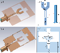
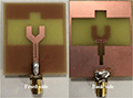
In this section, we first make an explanation for evolution principles of the plier-shaped radiated patch and then discuss design of slots and EBG loading for band-notch effects. Figure 1 illustrates the geometry of the overall UWB antenna. The front of the antenna consists of a wrench-shaped patch and feedline, on which a bent slot is etched to realize one rejected band, as can be seen in Figure 1(a). The ground is grooved and loaded with an EBG structure, as can be seen in Figure 1(c). The EBG strip is connected to the patch through a via with diameter D = 0.3 mm. We use FR-4 (e= 4.4) as substrate with a length L = 40 mm, width W= 32 mm, and a thickness oft = 1.2 mm. All design parameters are depicted in Figures 1(b) and (d) and are as listed in Table 1 for reference.
A. Design of the patch
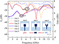
Figure 2 describes the optimization process of the patch and ground. The patch was initially square and the ground was also simply square grooved. A small size T-shaped slot was etched on the ground afterwards to slightly tune the resonant frequency, as shown in Ant. 2 of Figure 2. In order to realize a wider bandwidth, the patch shape was further optimized and the structure of Ant. 3 was proposed. The wrench-shaped patch succeeded in broadening the frequency band from 2.4 to 12 GHz along with the two T-shaped groove backside. It is obvious from Figure 2 that the S curve of Ant. 3 is the best among the three conditions because this configuration excited surface current more efficiently over the entire frequency band. The gains of antennas with the three different shapes are also shown in Figure 2.
Table 1: Dimensions of the proposed antenna
| Par. | Value (mm) | Par. | Value (mm) | Par. | Value (mm) |
| L | 40 | W | 30 | E | 5.8 |
| W | 32 | W | 6 | E | 1.4 |
| W | 2.6 | W | 3.5 | E | 2.2 |
| L | 16.9 | W | 1.8 | E | 2.6 |
| W | 10 | L | 15 | E | 1 |
| L | 10 | L | 4 | S | 0.8 |
| W | 4 | L | 5 | S | 7.4 |
| L | 6.5 | L | 5 | S | 0.3 |
| L | 2 | L | 16 | W | 0.4 |
| D | 0.3 | t | 1.2 | W | 0.3 |
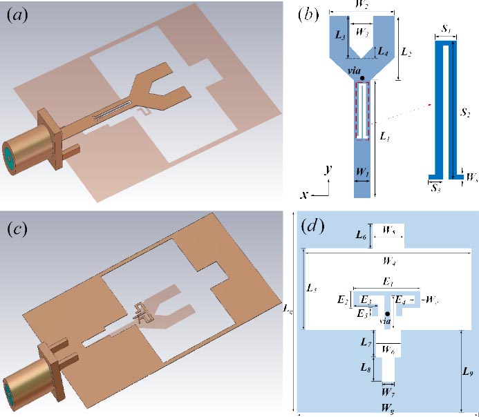
Figure 1: Geometry of the proposed antenna. (a) Top view of the antenna 3D model. (b) Description of the patch and feedline. (c) Bottom view of the antenna 3D model. (d) Description of the ground and EBG structure.
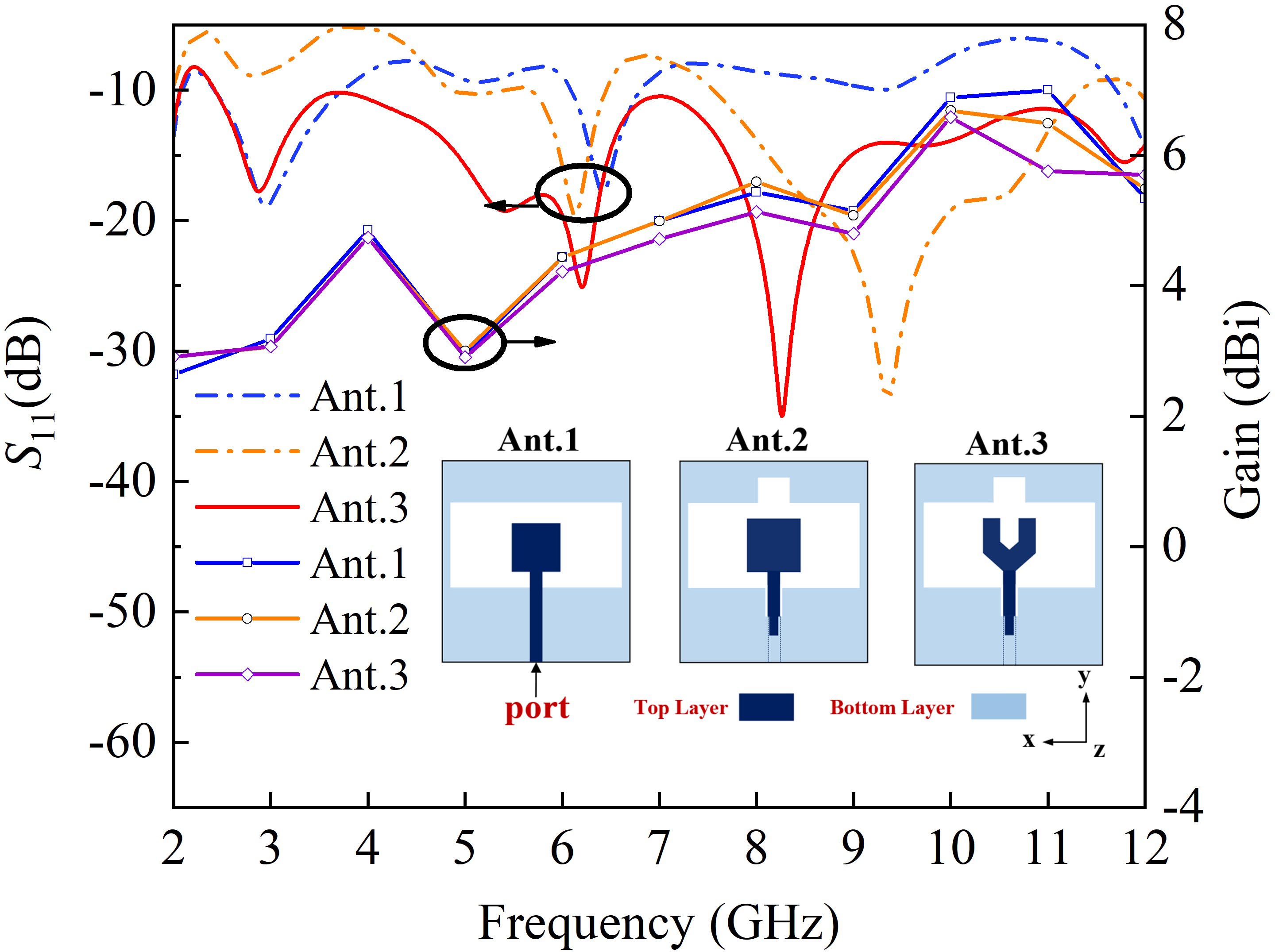
Figure 2: S and gain of antenna vs. evolution of patch.
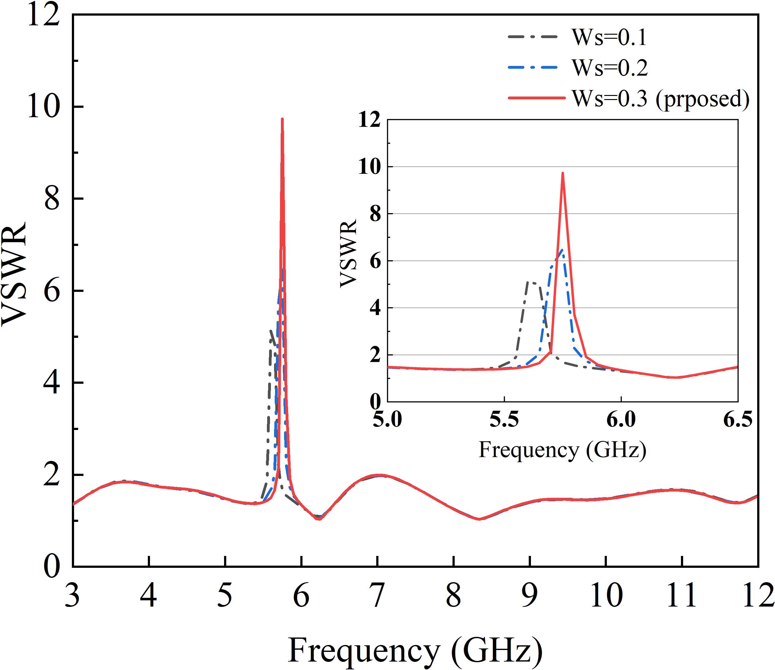
Figure 3: VSWR of antenna for different values of W.
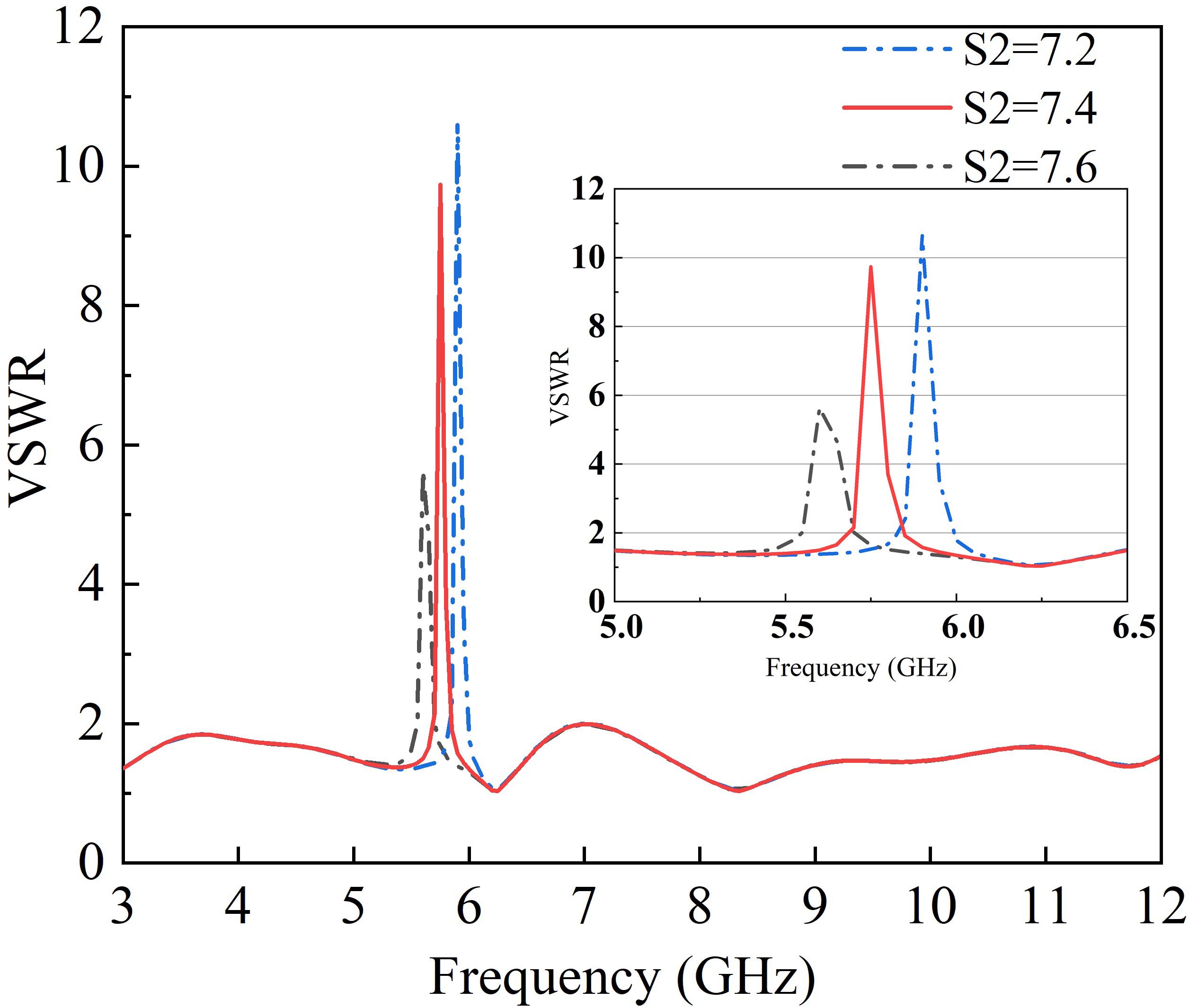
Figure 4: VSWR of antenna for different values of S.
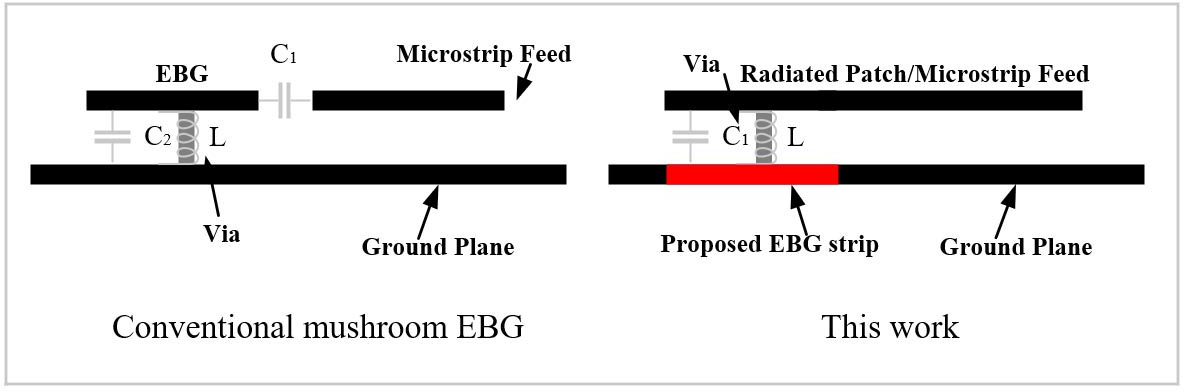
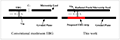
Figure 5: Schematic view of conventional EBG structure and this work. (a) Mushroom EBG. (b) This work.
B. Band-Notch techniques for upper WLAN band
Embedding varieties of slots on the feedline or patch of antenna to obtain notched band has been widely studied and applied. The slots can produce an effect equivalent to resonant circuit and conducive to the integration of the microstrip planar antenna. However, the length and width of slot as well as its position may generate distinct results.
In this work, thickness and permittivity of the substrate are taken into account during the UWB antenna design process. We calculated resonant frequency for 5.8 GHz through the following formula:
| (1) |
where is resonant frequency for notched band, c is the speed of light in vacuum, L is the sum of the physics length, and is the dielectric constant of antenna substrate. This equation does not mention the width of the slots; however, width of the slots may produce certain influence on resonant frequencies. Based on eqn (1), preliminary parameter values can be calculated, which, however, are far from satisfying. Regarding the shape and location of the slot, as well as the manufacturing process, the parameters must be further optimized.
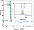
Based on the above analysis, a slot similar to shape was proposed. Figure 3 shows the VSWR simulation results for parameter W varying from 0.1 to 0.3 mm when the parameter S is fixed to 7.4 mm. In contrast, Figure 4 shows how the variation of parameter S tuned the notched band when W is fixed at 0.3 mm. It is not difficult to find out that width of slot and length of the slot determined the center frequency of the notched band jointly. It is determined that the center of notched band at 5.8 GHz is achieved when W is equal to 0.3 mm and S is equal to 7.4 mm, verifying that the stop band range of upper WLAN band (5.725–5.875 GHz)is achieved.
C. Study of Band-Notch techniques for lower WLAN band
Given the design of Part B, to realize another notch effect at the lower WLAN band (5.15–5.35 GHz), it is quite necessary to reduce the effect of coupling, especially for compact antennas. In the schematic structure diagram of the traditional mushroom-shaped EBG, as shown in Figure 5(a). The metallic EBG structure is etched on the top side of antenna and connected to the ground by via, which produced LC shunt circuit. In this article, we proposed an EBG structure as shown in Figure 5(b), the EBG strips and patch are separate and connected by via, which also forms an LC shunt circuit. The proposed EBG structure possessed EBG characteristic in terms of principle. In this sense, a novel EBG structure is proposed and built on the ground plane to realize the desired band-notch feature, meanwhile suppressing the coupling as was a filter.
As we all know, composite right/left-handed (CRLH) transmission line has been widely used to realize novel EBG design, and we used the interdigital method to realize a CRLH-EBG structure. Figure 6(a) illustrates the side view of the EBG structure and Figure 6(b) shows the plan view of it. The relationship between the size of the structure and resonant frequency can be expressed by the following formulas:
| (2) | ||
| (3) |
where n is odd, is the length of the open-loop, and f is the resonant frequency, namely, the length of the loop is a quarter of the resonant wavelength, or the electrical length is an odd multiple of p/2. The length of the proposed antenna is l/4 makes it a potential candidate for compact microstrip antenna application.
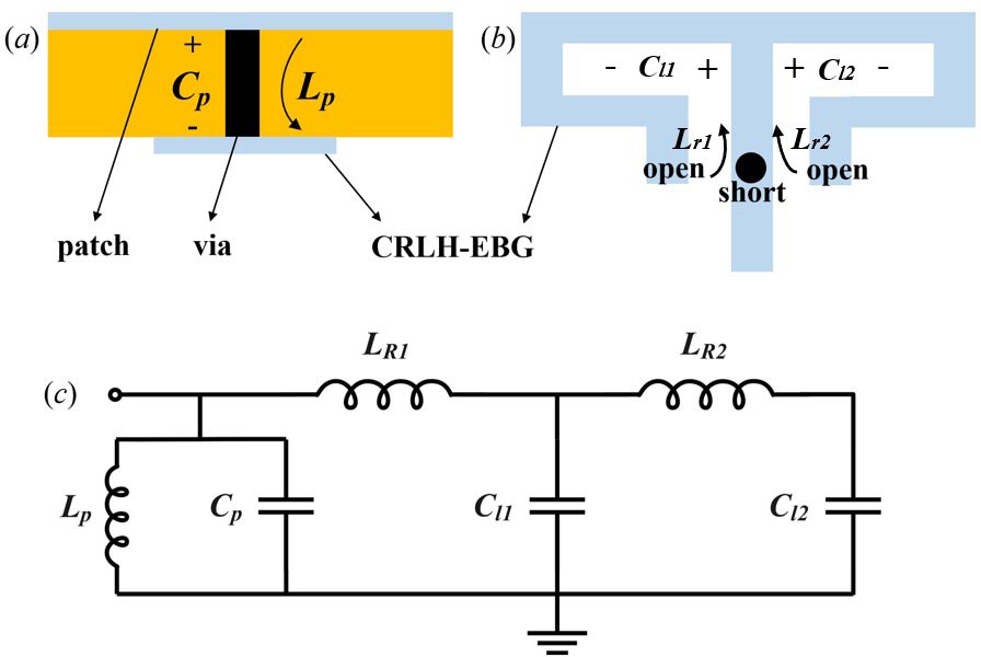
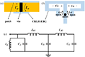
Figure 6: Principle of EBG structure. (a) Side view. (b) Top view of the EBG strip. (c) Equivalent circuit model.
To further understand the behavior of the CRLH-EBG structure in Figures 6(a) and (b), an equivalent circuit model is constructed in Figure 6(c). The via connecting the patch and the EBG structure in Figure 6(a) brings about parasite inductance and capacitance and, therefore, was modeled as L and C in Figure 6(c). It can be defined as right-hand capacitance and inductance. The generated capacitances C and C are used to characterize the left-handed capacitance and the shorted microstrip branch is used to characterize the left-handed inductances L and L, as shown in Figure 6(b). It is then obvious that the above resonant circuit represented a filter model, the resonant frequency of which is calculated to be 5.25 GHz, meaning impedance mismatch atthis point.
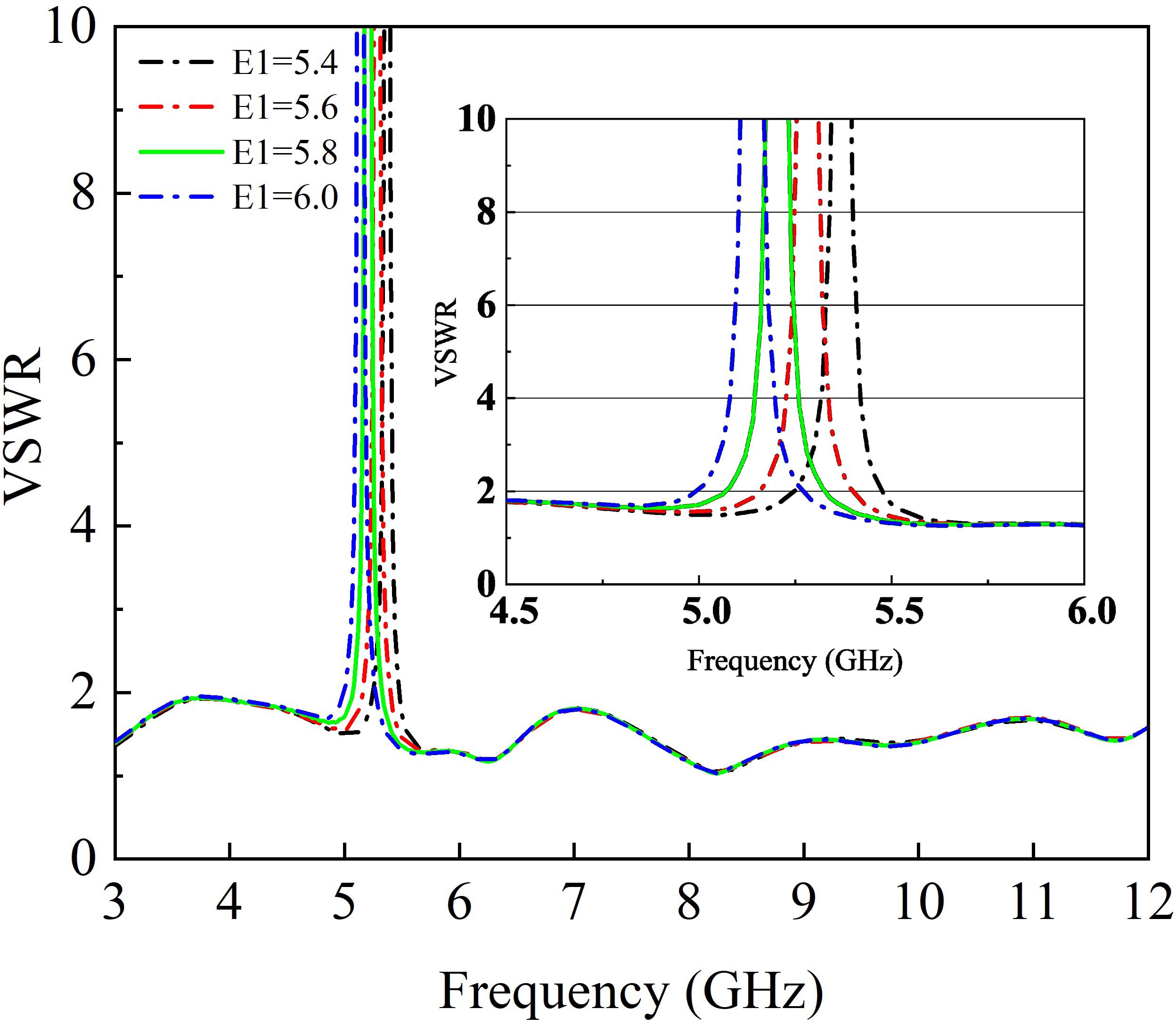
Figure 7: VSWR of antenna for different values of E.
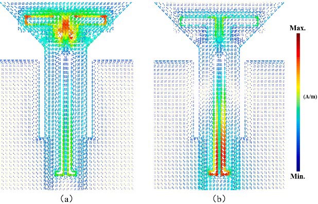
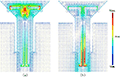
Figure 8: Surface current distribution of the proposed antenna at (a) 5.25 and (b) 5.8 GHz.
According to the above analysis and calculation, we have decided the value of E to be the most significant factor and its values should be limited between 5.4 and 6. Figure 7 exhibits the optimization process of parameter E. The simulated results of VSWR versus E demonstrate that the resonant frequency decreases as E increases, and the optimal value of Eshould be 5.8 mm.
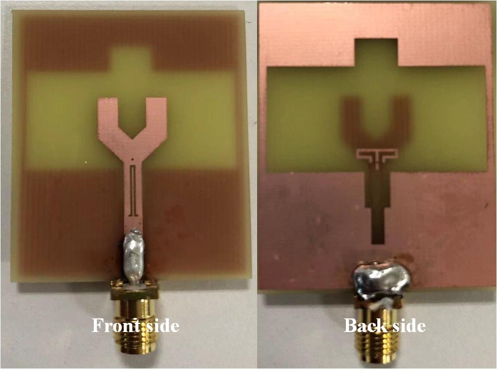
Figure 9: Photograph of the fabricated antenna.
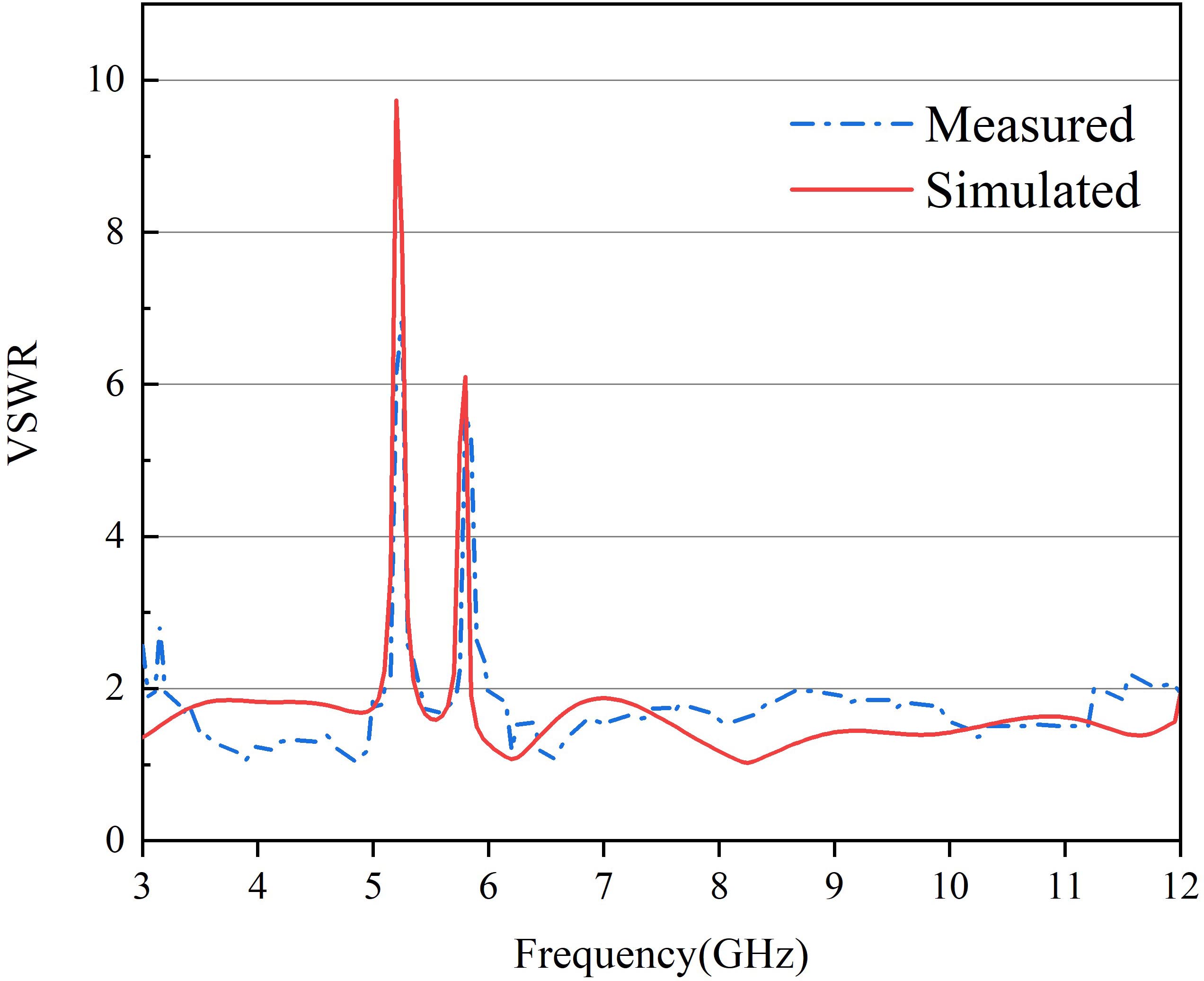
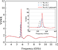
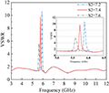
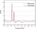
Figure 10: Simulated and measured VSWR of the proposed antenna.
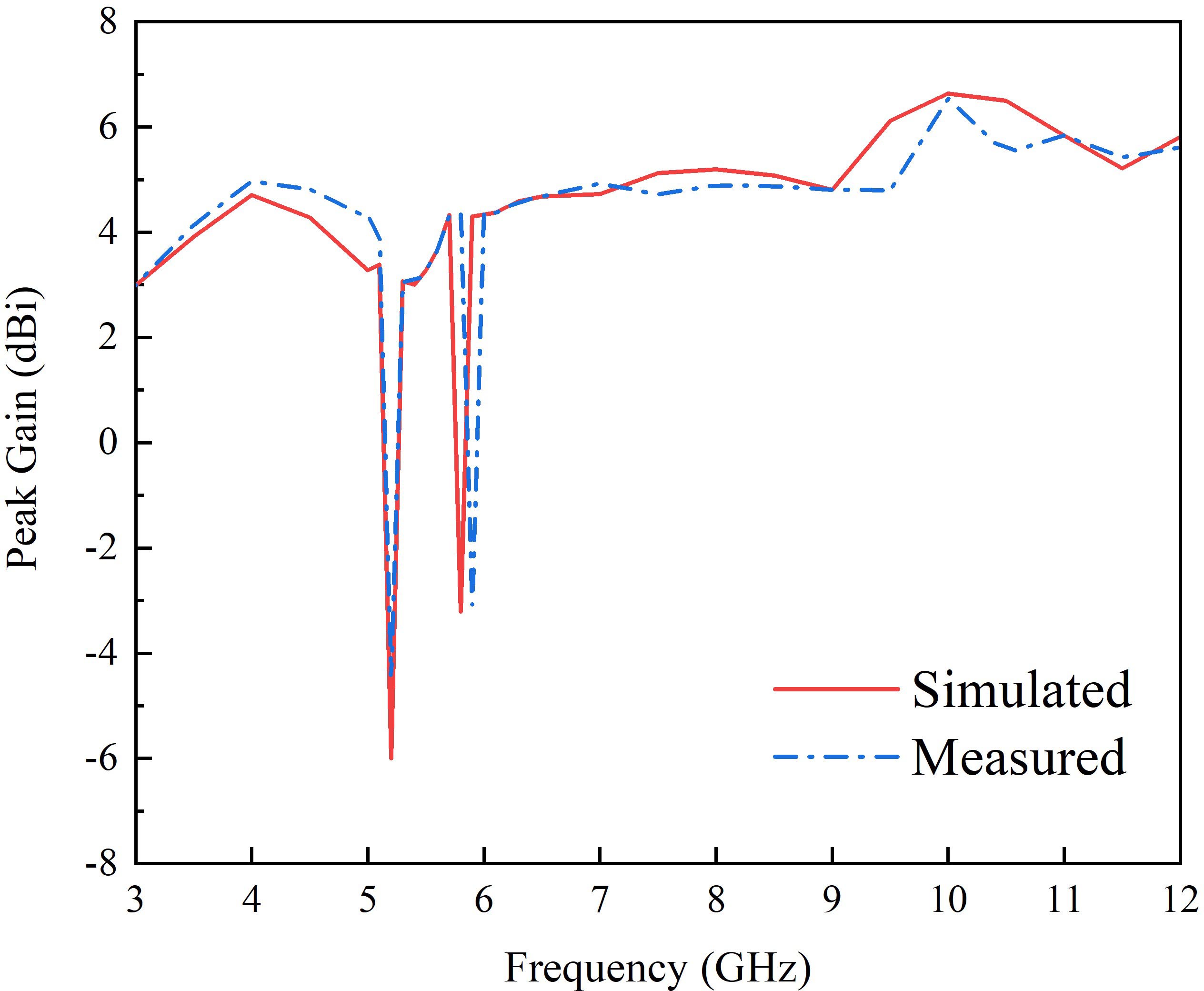
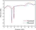
Figure 11: Simulated and measured gains of the proposed antenna.
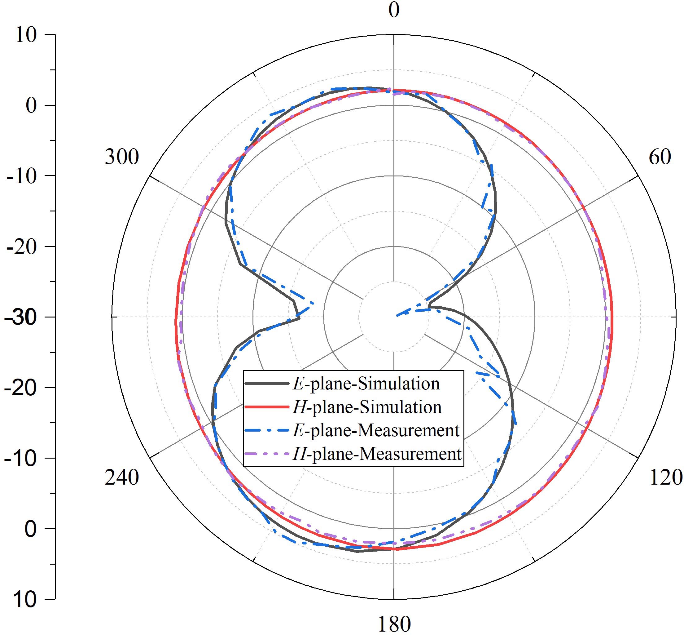
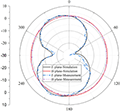
Figure 12: Simulated and measured radiation patterns in E- and H-plane at 3.5, 7.5, and 9 GHz, respectively.
Since the proposed notching structures are aimed at two adjacent frequencies, Figures 8(a) and (b) show the surface current distribution of the antenna at resonant frequencies of 5.25 and 5.8 GHz, respectively. In Figure 8(a), the CRLH-EBG structure proposed in this paper concentrates a strong current, whereas the Omega-shaped slot etched on the feeding line produces only a weak current, which can be drawn that the CRLH-EBG structure has an effect alone at 5.25 GHz. On the contrary, the obvious strong current distribution is generated at the edge of the Omega-shaped slot in Figure 8(b), while the EBG structure on the upper side has only gathered a small current concentration. It can be concluded that the slot achieves resonance at the 5.8-GHz frequency point and produces a notch effect. Furthermore, Omega-shaped slot formed a closed-loop resonant tank, while the proposed EBG structure formed an open-loop resonant tank. And they produced two different resonances. In summary, these two structures work independently and there exists almost no interaction between them.
III. MEASUREMENT AND DISCUSSION
The antenna prototype was fabricated and shown in Figure 11. It was measured with Agilent E8362B vector network analyzer. Figure 11 presents the simulated and the measured VSWR for the proposed antenna. Measured results show that the antenna provides an impedance bandwidth (VSWR 2) from 3.04 to 11.4 GHz except the notch band of 5.1–5.4 and 5.72–5.98 GHz.
The bandwidth requirement for UWB applications is satisfied, and the dual notched bands presented good notch characteristics for the lower (5.15–5.35 GHz) and upper (5.725–5.875 GHz) WLAN bands. Figure 11 shows the measured and simulated peak gain results. Both results are well-matched. It can be observed that the gain curve rises as the frequency increases, and the gain drops sharply at the notched frequency bands. Simulation and measurement are in good agreement.
The radiation pattern in E-plane (xz-plane) and H-plane (yz-plane) at 3.5, 7.5, and 9.5 GHz of measured and simulated results are shown in Figure 12. The proposed antenna presents an omni-directional characteristic in H-plane and bi-directional patterns in E-plane for all simulated and measured results.
IV. CONCLUSION
The proposed wrench-shaped UWB antenna has realized an impedance bandwidth of 3.04–11.4 GHz. The approaches of etching an Omega-shaped slot on the feedline and building a novel CRLH-EBG structure have achieved notched features at uplink (5.725–5.875 GHz) and downlink (5.15–5.35 GHz) of WLAN frequency bands, respectively. There is almost no interference between these two structures. Measured and simulated results of the proposed antenna are in good agreement substantially. The peak gain value of the proposed antenna is 6.53 dBi, while it sharply decreases to –4.5 dBi at notched bands.
ACKNOWLEDGMENT
This work was supported by the Educational Department of Fujian Province under Grant JAT210214 and Grant JAT190298, National Fund Cultivation Program of Jimei University under Grant ZP2020035 and Youth Top Talent Program of Jimei University under Grant ZR2019001.
REFERENCES
[1] M. S. Khan, A. Iftikhar, R. M. Shubair, A. D. Capobianco, B. D. Braaten, and D. E. Anagnostou, “Eight-element Compact UWB-MIMO/diversity Antenna with WLAN Band Rejection for 3G/4G/5G Communications,” IEEE Open J. Antennas Propag., vol. 1, pp. 196-206, 2020.
[2] C. C. Rong, W. Xiao, Y. H. Xu, and M. Y. Xia, “A Double Band-notched UWB Antenna for Flexible RF Electronics,” Applied Computational Electromagnetics Society (ACES) Journal, vol. 32, no. 5, pp. 413-417, Jan. 2017.
[3] R. Gupta, M. M. Patel, S. Tanwar, N. Kumar, and S. Zeadally, “Blockchain-based Data Dissemination Scheme for 5G-enabled Softwarized UAV Networks,” IEEE Trans. Green Commun. Networking, vol. 5, no. 4, pp. 1712-1721, Dec. 2021.
[4] X. J. Liao, H. C. Yang, N. Han and Y. Li., “UWB Antenna with Dual Narrow Band Notches for Lower and Upper WLAN Bands,” Electron. Lett., vol. 46, no. 24, Nov. 2010.
[5] Y. Jia, S. Jin, and P. Savi, “GNSS-R Soil Moisture Retrieval Based on a XGboost Machine Learning Aided Method: Performance and Validation,” Remote Sens., vol. 11, no. 14, 2019.
[6] M. K. Shereen, M. I. Khattak and J. Nebhen, “A Review of Achieving Frequency Reconfiguration through Switching in Microstrip Patch Antennas for Future 5G Applications,” Alexandria Engineering Journal, vol. 61, no. 1, pp. 29-40, 2021.
[7] G. Gao, B. Hu and J. Zhang, “Design of a Miniaturization Printed Circular-slot UWB Antenna by the Half-cutting Method,” IEEE Antennas Wirel. Propag. Lett., vol. 12, pp. 567-570, 2013.
[8] G. Teni, N. Zhang and J. Qiu, “Research on a Novel Folded Monopole with Ultrawideband Bandwidth,” IEEE Antennas Wirel. Propag. Lett., vol. 13, pp. 802-805, 2014.
[9] C. Dikmen, S. Cimen, and G. Cakir, “Design of Double-sided Axe-shaped Ultra-wideband Antenna with Reduced Radar Cross-section,” IET Microwaves Antennas Propag., vol.8, pp. 571-579, 2014.
[10] H. Zhu and Q. X. Chu, “Ultra-wideband Bandpass Filter with a Notch-band Using Stub-loaded Ring Resonator,” IEEE Microwave Wirel. Compon. Lett., vol. 23, no. 7, pp. 341-343, July 2013.
[11] T. Sedghi, V. Rafii, and M. Moosazadeh, “UWB Monopole Antenna with Compact Polygon-shaped Patch for Portable Devices,” Applied Computational Electromagnetics Society (ACES) Journal, vol. 29, no. 1, pp. 67-70, Jan. 2014.
[12] W. C. Weng and M. C. Chang, “Ultra-wideband Planar Log-periodic Slot Antenna with Exponential Shapes on Slot Edges,” Applied Computational Electromagnetics Society (ACES) Journal, vol. 34, no. 9, pp. 1280-1286, Sep. 2019.
[13] S. H. Yeung, K. F. Man and W. S. Chan, “Multiple Circular-sector Structures for Wideband Planar Monopole Antenna Designs Covering 146% fractional bandwidth,” IEEE Antennas Propag. Mag., vol. 54, no. 1, pp. 76-94, Feb. 2012.
[14] A. Taibi, M. Trabelsi and A. A. Saadi, “Efficient Design Approach of Triple Notched UWB Filter,” AEU – I. J. Electron. Commun., vol. 131, March 2021.
[15] W. Jiang and W. Che, “A novel UWB Antenna with Dual Notched Bands for WiMAX and WLAN Applications,” IEEE Antennas Wirel. Propag. Lett., vol. 11, pp. 293-296, 2012.
[16] R. Aldhaheri, I. Alruhaili, K. Babu and M. Sheikh, “A Compact CPW-fed UWB Antenna with Dual-band Notched Characteristics for WiMAX/WLAN Applications,” Applied Computational Electromagnetics Society (ACES) Journal, vol. 36, no. 2, pp. 145-151, 2021.
[17] J. Y. Siddiqui, C. Saha and Y. M. M. Antar, “Compact Dual-SRR-loaded UWB Monopole Antenna with Dual Frequency and Wideband Notch Characteristics,” IEEE Antennas Wirel. Propag. Lett., vol. 14, pp. 100-103, 2015.
[18] M. Yazdi and N. Komjani, “Design of a Band-notched UWB Monopole Antenna by Means of an EBG Structure,” IEEE Antennas Wirel. Propag. Lett., vol. 10, pp. 170-173, 2011.
[19] F. Alizadeh, C. Ghobadi, J. Nourinia and H. Abdi, B. Mohammadi, “UWB Dual-notched Planar Antenna by Utilizing Compact Open Meander Slitted EBG Structure,” AEU-I. J. Electron. Commun., vol. 136, July. 2021.
[20] Q. Li, Y. F. Sun and H. Y. Fang, “Compact ACS-fed UWB MIMO Antenna with Dual Band Notches,” Applied Computational Electromagnetics Society (ACES) Journal, vol. 36, no. 1, pp. 55-60, Jan. 2021.
[21] L. Y. Chen, W. S. Zhou, J. S. Hong and M. Amin, “A Compact Eight-port CPW-fed UWB MIMO Antenna with Band-notched Characteristic,” Applied Computational Electromagnetics Society (ACES) Journal, vol. 35, no. 8, pp. 887-892, Jan. 2020.
[22] M. Ghahremani, “Miniaturised UWB Antenna with Dual-band Rejection of WLAN/WiMAX Using Slitted EBG Structure,” IET Microwaves Antennas Propag., vol. 13, no. 3, pp. 360-366, 2019.
[23] E. Thakur, N. Jaglan and S.D. Gupta, “Design of Compact Triple Band-notched UWB MIMO Antenna with TVC-EBG Structure,” J. Electromagn. Waves Appl., vol. 34, pp. 1-15, 2020.
[24] P. P. Bhavarthe, S. S. Rathod and K. T. V. Reddy, “A Compact Dual Band Gap Electromagnetic Band Gap Structure,” IEEE Trans. Antennas Propag., vol. 67, no. 1, pp. 596-600, Jan. 2019.
[25] B. Feng, L. Li, J. Cheng and C. Sim, “A Dual-band Dual-polarized Stacked Microstrip Antenna with High-isolation and Band-notch Characteristics for 5G Microcell Communications,” IEEE Trans. Antennas Propag., vol. 67, no. 7, pp. 4506-4516, Jul. 2019.
[26] L. Peng, B. J. Wen, X. F. Li, X. Jiang and S. M. Li, “CPW Fed UWB Antenna by EBGs with Wide Rectangular Notched-band,” IEEE Access, vol. 4, pp. 9545-9552, 2016.
BIOGRAPHIES

Tongyu Ding was born in Heilongjiang, China, in 1987. He received the M.S. degree from the Harbin Institute of Technology, Harbin, China, and the Ph.D. degree in electronics and communication engineering from the Politecnico di Torino, Turin, Italy, in 2011 and 2015, respectively.
He is currently an Associate Professor with the School of Ocean Information Engineering, Jimei University, Xiamen, China. His recent research interests include antennas and numerical techniques for 5G wireless communications.

Mengyu Wang was born in Anhui province, China. He received the bachelor’s degree from Huainan Normal University, Anhui, China, in 2019. He is currently working toward the master’s degree in information and communication engineering with Jimei University, Xiamen, China.
His research activities include antennas and millimeter wave channel modeling.

Jie Guo was born in Shaanxi province, China, in 2018. He received the bachelor’s degree from the Xi’an University of Posts & Telecommunications, Shaanxi, China, in 2021. He is currently working toward the master’s degree in information and communication engineering with Jimei University, Xiamen, China.
His research activities include the directional bipolarization antenna system and reconfigurable intelligent surface.

Liang Zhang received the B.S. degree in communications engineering and the M.S. and Ph.D. degrees in microelectronics and solid-state electronics from the Harbin Institute of Technology, Harbin, China, in 2004, 2007, and 2013,respectively.
After graduation, he joined Xiamen University, Xiamen, China, as a Postdoctoral Fellow. Currently, he is an Associate Professor with Jimei University, Xiamen, China. His recent research interests mainly include novel RADAR systems, smart antennas, and reconfigurable intelligent surface.

Jun Xiao received the B.S. and M.S. degrees from the Harbin Institute of Technology, Harbin, China, and the Ph.D. degree from the Beijing University of Posts and Telecommunications, Beijing, China,respectively.
In 2019, he joined the School of Ocean Information Engineering, Jimei University, Xiamen, China. His current research interests include millimeter-wave antennas and THz antennas.
ACES JOURNAL, Vol. 37, No. 3, 297–304.
doi: 10.13052/2022.ACES.J.370306
© 2021 River Publishers