A Novel Compact Filtering Antenna for 5.0-GHz WLAN Communication System
Shujia Yan1, Chongqi Zhang1, Qiang Chen1, and Mei Song Tong2
1School of Electronic and Electric Engineering, Shanghai University of Engineering Science, Shanghai, China
2Department of Electronic Science and Technology, Tongji University, Shanghai, China
mstong@tongji.edu.cn
Submitted On: January 16, 2022; Accepted On: October 30, 2022
Abstract
The proposed antenna presents a microstrip filter antenna with both filter out-of-band rejection characteristics and antenna radiation characteristics for WLAN communication system. The antenna consists of four U-shaped microstrip resonators, one -shaped antenna, and one parallel coupling line. The -shaped antenna has the filtering function as the last order resonator, and the parallel coupling line integrates the filter and antenna as the conductance converter. After simulation and test, the results show that the center frequency of the filter antenna is GHz, the fractional bandwidth is ( GHz), the in-band gain changes smoothly, the maximum in-band gain is dBi, the gain at MHz outside the passband rapidly decreases to dBi, and the overall out-of-band gain drops to below dBi. The filter antenna has a simple structure and thin substrate, which optimizes the overall size of the filter and antenna, reduces the transmission loss between them, and is applicable to the RF front-end of wireless communication systems.
Index Terms: compact design; filter antenna; microstrip antenna; WLAN communication system
I. INTRODUCTION
In recent years, the rapid development of wireless communications has led to an exponential growth in the demand for passive devices. As one of the most widely used wireless communication systems, WLAN technology has become more and more mature. The data transmission rate in the -GHz band ( GHz) of the IEEE802.11a standard is relatively high, so it is able to meet the needs of most high-speed communications and, therefore, has been widely used. As an important part of wireless communication system, antennas and filters play a very important role in the performance of the whole wireless communication system, but their size is often much larger than other devices. If antennas and filters are integrated in a compact module that provides both radiation and filtering functions, the size of the communication system could be effectively reduced and the communication quality could be improved by reducing mutual interference. Therefore, filtering antennas [1] that combine filters and antennas closely together have been widely studied.
In the traditional design method of filtering antenna, the antenna and filter are designed separately based on the reference impedance, which is or , and then they are connected directly because they share a common characteristic impedance. However, this will easily cause impedance mismatch and increase the insertion loss of the circuit, leading to the deterioration of the entire system. To eliminate this problem, an additional structure for impedance transformation is used between the filter and the antenna [2, 3], so that the filter can be correctly integrated with the antenna in the required bandwidth with good impedance matching. However, this structure increases the circuit area and transmission loss in the frequency range. Also, Bailey proposed a microstrip antenna with filtering characteristics by coupling four layers of patches to each other [4]. However, none of the above methods use an integrated design approach and there is no generality. In 2016, Fakharian et al. proposed an open/short-ended digital E-type resonator by using two integrated PIN diodes and realized the coupling connection between the filter and the antenna [5], but it cannot be printed directly. Moreover, the method of deploying simple parasitic elements was proposed to expand the working bandwidth of the antenna by improving the roll-off performance of the upper edge of the radiator and the selectivity of the upper and lower edges [6, 7, 8]. Nevertheless, the above antenna only has onepolarization.
More advanced filtering antennas based on the substrate integrated waveguide were proposed in [9, 10] and they have shown good filtering effects, but manufacturing the antenna becomes more difficult and requires a much higher cost. Although the comprehensive design method is adopted, the coupling structure between the antenna and filter is more complicated and manufacturing it is not easy [11]. In addition, a filter antenna consisting of a sector patch antenna and a bandpass filter is proposed in [12], which has a smooth in-band gain but very limited out-of-band rejection. More recently, a integrated filtering antenna array with good out-of-band suppression characteristics was proposed, but unfortunately, its impedance bandwidth cannot cover the entire -GHz band of the WLAN communication system [13].
Given the above problems, this paper proposes a new type of microstrip filtering antenna for WLAN communication systems. The filtering antenna is designed through a comprehensive design method and integrates four U-shaped open-loop resonators, a -shaped antenna, and a section of coupling line. The -shaped antenna, as the last resonator of the filter, has both radiation characteristics and filtering characteristics. Simulation and measurement results show that the filtering antenna has a center frequency of GHz and a maximum gain of dBi. Also, it has a gentle change of in-band gain and the maximum gain difference is dBi. Furthermore, its out-of-band gain can decrease rapidly and stabilize at dBi finally, showing an excellent filtering feature. The filtering antenna not only presents good radiation and filtering characteristics, but also has a compact size. The overall size is mm mm mm, which is much smaller than that of other structures [13]–[15]. With the attractive performance, the filtering antenna could be very useful in the -GHz band of WLAN communicationsystem.
II. CONFIGURATION OF ANTENNA
A. Filter selection
An open-circuit resonator with a length that is an integer multiple of the half wavelength has the characteristics of a parallel resonant circuit. To realize the integrated design of the filtering antenna, the U-shaped filter is selected. The filter has a compact structure with good indicators and has been widely used in RF and microwave engineering. Moreover, the U-shaped filter uses a traditional open-loop resonator as the basic resonance unit and the open-loop resonator is equivalent to a half-wavelength resonator. A fifth-order bandpass filter is designed by using the design method of integrated filter. The filter has a center frequency of GHz, a fractal bandwidth of , and a ripple coefficient of dB, respectively. The dielectric plate is Rogers with a dielectric constant of and a plate thickness of mm. The coupling coefficient of the resonator and the external quality factor at the input and output can be calculated by [16].
| (1) | ||
| (2) | ||
| (3) |
In the above equations, represents the coupling coefficient between -th and -th resonators, FBW represents the fractal bandwidth, and with represent the Chebyshev normalized component values as shown in Table 1 [16], where represents the external figure of merit at the input and represents the external figure of merit at the output, respectively. From the formulas, we can obtain the coupling coefficients as and , and the -factors at the input and output as , respectively.
Table 1: Chebyshev Normalized Component Values
| n | ||||||
|---|---|---|---|---|---|---|
| 1 | 0.096 | 1.0 | ||||
| 2 | 0.4489 | 0.4078 | 1.0 | |||
| 3 | 0.6292 | 0.9703 | 0.6292 | 1.0 | ||
| 4 | 0.7129 | 1.2004 | 1.3213 | 0.6476 | 1.0 | |
| 5 | 0.7563 | 1.3049 | 1.5773 | 1.3049 | 0.7563 | 1.0 |
B. Determination of the filter’s sizes
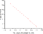
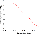
To determine the physical sizes of the open-loop resonator, a single-port simulation model is created by using the well-known simulation tool HFSS, and the simulation is performed in an eigenmode. The resonant frequencies of the resonator with different values of are obtained and shown in Fig. 1. It can be seen from the figure that the resonant frequency decreases as the length of the resonator increases. To achieve a resonant frequency of GHz, the length of the resonator is initially set to be mm.
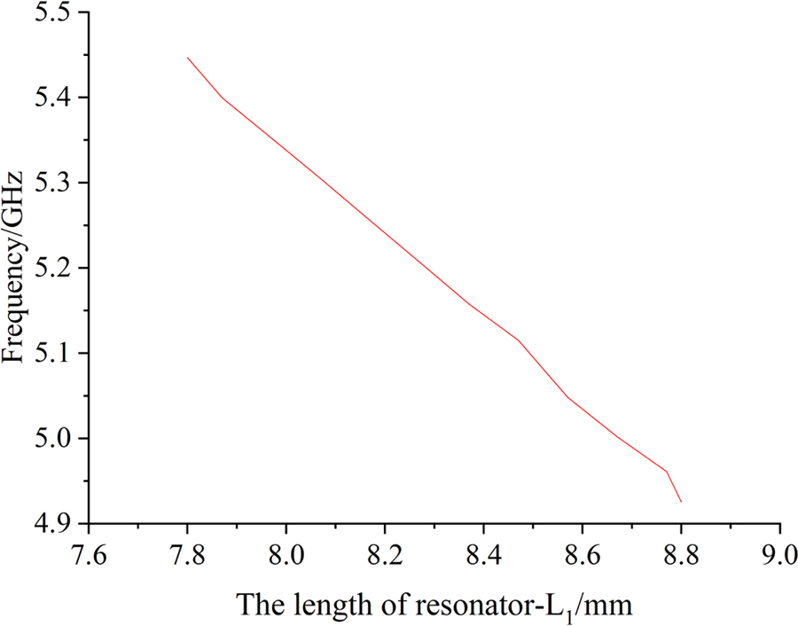
Fig. 1: Change of resonant frequency in terms of .
After the length of the resonator is set, the coupling coefficient between the resonator and the external quality factor of the output resonator is extracted by the comprehensive design method, and then the specific sizes of the filter can be determined with the simulations of HFSS. For mutual coupling resonators, the required coupling coefficient can be obtained by adjusting the coupling structure’s parameters. Because the U-shaped filter keeps aligned up and down, the coupling strength of the resonators is determined by the size of gap between the resonators. The coupling coefficient can be calculated by [16].
| (4) |
where and are the upper and lower resonant frequency of the coupled resonator, respectively. Also, the center frequency is and the coupling coefficient is positively related to the distance between the two resonance peaks [17].
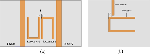
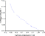
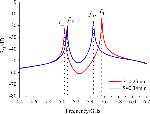
A simulation is performed with the length of mm and the simulation model is shown in Fig. 2 (a). The relationship between the gap of filtering resonators and the coupling coefficient is obtained and shown in Fig. 3. It can be seen that the coupling coefficient increases as the coupling gap decreases. When the gap between the resonators is mm and mm, the corresponding resonance curves are shown in Fig. 4. The calculated coupling coefficients are and , respectively, which can meet the need very well.
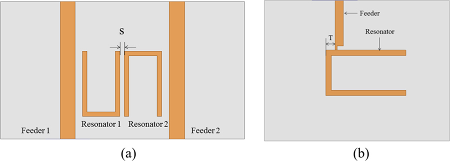
Fig. 2: Simulated parameters for (a) the gap of resonators and (b) the tap position .
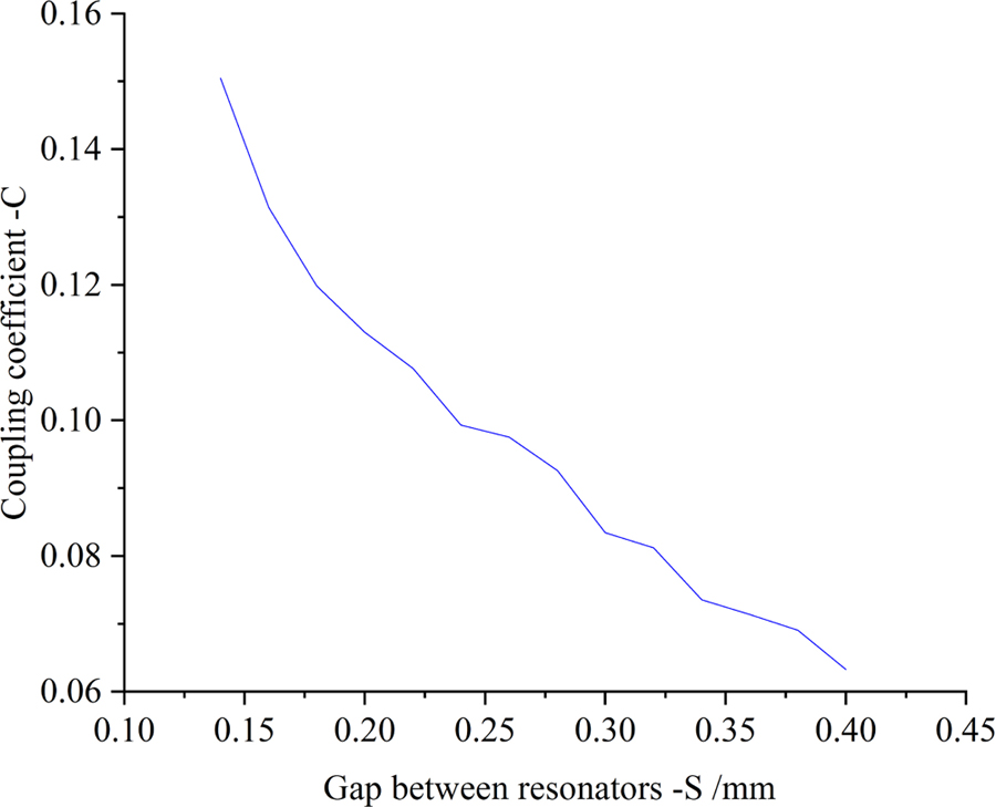
Fig. 3: Relationship between the gap of resonators and coupling coefficient .
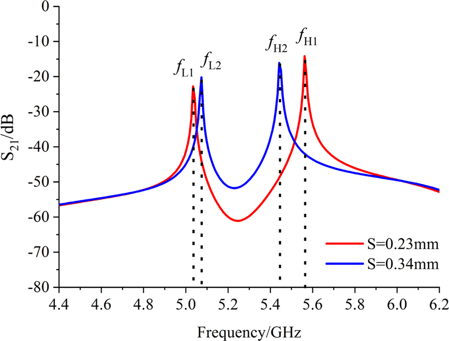
Fig. 4: Resonant responses of the two open-loop resonators.
Because the fractal bandwidth of the filter is designed to be , which is relatively wide, and the traditional slot-coupled feeding structure is thought of as complicated, we use a tap line to feed directly in the filter design so that the external figure of merit can be adjusted by changing the parameters of feeding structure. The external figure of merit of a resonator is mainly determined by the tap’s feeding position at both ends in the filter. To obtain the required figure of merit, a single-port simulation is performed with a single resonator and the simulation model is shown in Fig. 2 (b). The external figure of merit is calculated by [16].
| (5) |
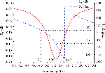
where represents the resonant frequency of the resonator and represents the difference of frequencies corresponding to the phases of higher and lower than the phase at . When the resonator’s length is determined, the single-port simulations are performed by taking different values for the tap position . The changing curve of the external quality factor in terms of the tap position is shown in Fig. 5 and it can be seen that is inversely related to . When mm, the changing curve of the amplitude and phase of the is shown in Fig. 6. According to Equation (5), the external figure of merit is , which basically meets the requirement.
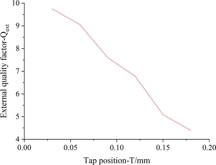
Fig. 5: Relationship between Q and T.
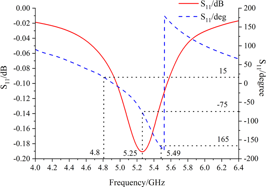
Fig. 6: Amplitude and phase of S when T = 0.09 mm.
C. Optimization of the filter
In the previous design and analysis, the structural parameters of the filter are preliminarily determined, i.e., the resonator’s length is mm, the tap position is mm, and the coupling gaps are mm and mm, respectively. The model of initial filter is established in the HFSS and then optimized for each structural parameter. The optimized structure is shown in Fig. 7 and its -parameter is plotted in Fig. 8. It can be seen that the range of dB bandwidth is from GHz to GHz, the center frequency is GHz, the reflection coefficient is greater than dB, and the insertion loss is less than dB, which can meet the design requirements fully.
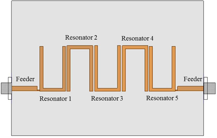
Fig. 7: Structure of the optimized filter.
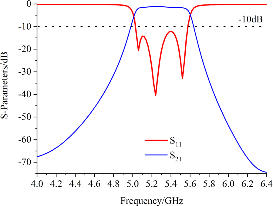
Fig. 8: parameter of the optimized fifth-order filter.
D. -shaped antenna and its integration with the filter
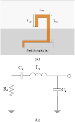
The -shaped antenna is a deformed monopole antenna, the structure and equivalent circuit of which are shown in Fig. 9. In the figure, is the radiation resistance of the antenna, is the resonance capacitance, is the resonance inductance, and is the added parallel capacitance which is used to maintain the same impedance characteristic as that of the antenna in a wider bandwidth [17]. The antenna and the filter’s circuit board have a common ground, and an impedance conversion line is connected to the microstrip antenna. The line can adjust the resonance characteristic of the antenna at GHz and the antenna actually becomes the last resonator of the filter. The antenna needs to have the same figure of merit as the filter, and the external figure of merit of the antenna can be extracted by [17].
| (6) |
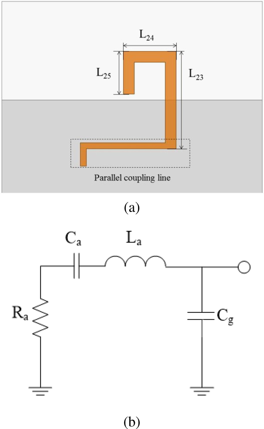
Fig. 9: Antenna part of the proposed filtering antenna. (a) Structure. (b) Equivalent circuit.
where is the corresponding frequency with the maximum value of resistance and is the input impedance at the antenna’s feeding point. The resonance frequency of the -shaped antenna is determined by the total length of , , and , and it is approximately the half wavelength at the center frequency. From the simulations, we find that the current density in the vertical arm connected to the coupling line is the strongest and it is shown in Fig. 10. Also, the length can be adjusted to obtain a matching figure of merit while keep the total length unchanged approximately.
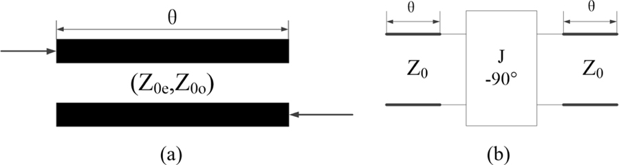
Fig. 10: Current density distribution of the antenna.
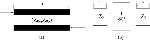
After designing the bandpass filter and the -shaped antenna, we then use a couple of parallel coupling lines as an admittance transformer to connect the filter with the antenna. The parallel coupling lines and their equivalent circuit are shown in Fig. 11 [18].

Fig. 11: A couple of parallel coupling lines. (a) Structure. (b) Equivalent circuit.
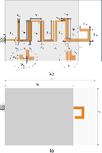
Table 2: Structural Parameters of the Filtering Antenna (unit: mm)
| L | ||||||||
|---|---|---|---|---|---|---|---|---|
| 41.49 | 31.59 | 5 | 0.47 | 8.17 | 8.23 | 8.3 | 2.34 | 9.66 |
| W | ||||||||
| 9.84 | 5.34 | 2.34 | 26.25 | 0.9 | 0.2 | 0.6 | 1.1 | 0.26 |
| T | B | |||||||
| 0.37 | 0.18 | 0.08 | 5 |
The parity analysis method is used to analyze the parallel coupling lines. If the two structures have the same electrical properties, the ABCD matrices of the two structures should be equal. When the electrical length is , we can obtain the following relationship
| (7) | ||
| (8) | ||
| (9) |
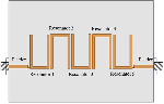
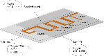
where and are the even- and odd-mode impedances, respectively, is the input impedance, and and are the original values of the filter. The even- and odd-mode impedances can be obtained when is given, and the physical dimensions of the parallel coupling lines can then be determined. When all structural parameters of the filtering antenna are determined, the overall optimization can be performed in the HFSS. The complete structure of the filtering antenna is shown in Fig. 12 and it has three layers. The middle layer is the substrate and the bottom of the substrate is a ground plate which is made of copper. Also, the copper’s resonance unit and the antenna are attached to the upper layer of the substrate. The parameters of overall structure are shown in Fig. 13, and the specific values of those parameters are listed in Table 2.

Fig. 12: Complete structure of the filtering antenna.
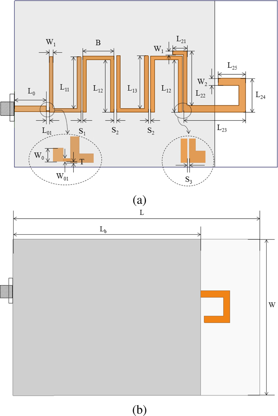
Fig. 13: Structural parameters of the filtering antenna. (a) Top view. (b) Back view.
III. PERFORMANCE OF THE FILTERING ANTENNA
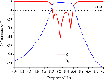
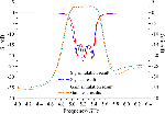
The physical PCB board of the filtering antenna is manufactured according to the structural parameters obtained from the optimization simulations and it is shown in Fig. 14. The parameter and gain of the filtering antenna are measured using a vector network analyzer and the comparison between the simulation results and measurement results are illustrated in Fig. 15. From the figure, we can see that the center frequency of the filtering antenna is GHz, the fractal bandwidth at dB is ( GHz), and the return loss is lower than dB. There is a small frequency offset in the measurement result due to the inevitable errors in the experimental setup and manufacturing of PCB board. In addition, the gain of the filtering antenna is dBi at the frequency of GHz and the change of in-band gain is gentle because the maximum deviation of gain is only dBi. Outside the band, the gain drops to dBi at MHz and the gain drops overall to dBi finally.

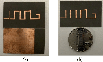
Fig. 14: Proposed filtering antenna. (a) Physical image. (b) Size comparison.
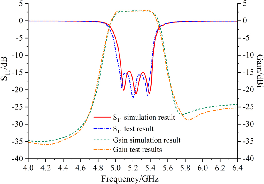
Fig. 15: parameter and gain of the filter antenna.
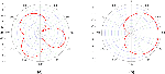
We also present the radiation patterns of the filtering antenna at GHz by simulations and they are shown in Fig. 16. In the XOY plane, there is an 8-shaped pattern similar to that of a monopole antenna. Moreover, there is a depression in the direction of and it is mainly caused by the coupling loss between the antenna’s end and the ground plate.
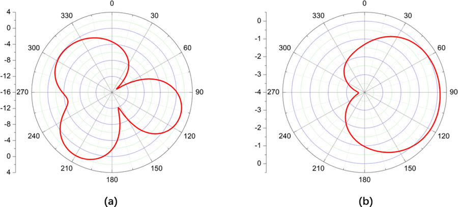
Fig. 16: Simulated radiation patterns of the filtering antenna. (a) XOY plane. (b) YOZ plane.
We compare the antenna proposed in this paper with the typical antennas proposed in previous papers and the result is shown in Table 3. It can be seen that the filter antenna proposed in this paper has higher gain than the antenna proposed in [14], much smaller physical size than those antennas proposed in [19]–[22], and wider bandwidth than the antenna proposed in [23]. The bandwidth of proposed antenna can cover the - GHz band to meet the requirements of practical applications.
Table 3: Comparison on the Performances od Antennas
| Reference | BW (GHz) | Size (mm) | Gain (dBi) |
|---|---|---|---|
| [14] | 3.1-10.6 | 40 × 30 | 3.05 |
| [19] | 3.5-5.97 | 49 × 37.85 | 4.177 |
| [20] | 5.15-5.825 | 64.3 × 34.8 | 3.5 |
| [21] | 5.15-5.825 | 98.93 × 42.93 | 7.40 |
| [22] | 5.15-5.825 | 93.53 × 38.82 | 7.30 |
| [23] | 5.25-5.35 | 21.075 × 17 | 3.93-4.45 |
| This work | 5-5.42 | 41.49 × 26.25 | 3.059 |
*The gain is obtained in the band of GHz.
IV. CONCLUSION
This paper proposes a microstrip filtering antenna for WLAN communication system in the -GHz band by using an integration design method of filters. The antenna becomes the fifth-order resonator of the filter through the integration of parallel coupling lines, which realize the combination of antenna’s radiation property and filter’s out-of-band rejection characteristic. The simulation and measurement results show that the filtering antenna has a smooth in-band gain and good out-of-band suppression feature. Also, the antenna has a compact structure whose overall size is much smaller than that of other structures. Based on the excellent performance, the proposed filtering antenna can be a good candidate for WLAN communication system in the -GHz working band.
REFERENCES
[1] Y. F. Cao, Y. Zhang, and X. Y. Zhang, “Filtering antennas: from innovative concepts to industrial applications,” Frontiers of Information Technology & Electronic Engineering, vol. 21, no. 1, pp. 116-127, 2020.
[2] M. Troubat, S. Bila, M. Thévenot, D. Baillargeat, T. Monédière, S. Verdeyme, and B. Jecko, “Mutual synthesis of combined microwave circuits applied to the design of a filter-antenna subsystem,” IEEE Transactions on Microwave Theory and Techniques, vol. 55, no. 6, pp. 1182-1189, Jun. 2007.
[3] W.-J. Wu, S.-L. Zuo, X.-M. Huang, D.-E. Wen, and R. Fan, “Compact dual-band loop-loaded monopole with integrated band-select filter for WLAN application,” IEEE International Symposium on Antennas, Propagation and EM Theory, Xi’an, China, Oct. 2012.
[4] M. C. Bailey, “A stacked patch antenna design with strict bandpass filter characteristics,” 2004 IEEE International Symposium on Antennas and Propagation and USNC/URSI National Radio Science Meeting, vol. 2. Monterey, CA, USA,Jun. 2004.
[5] M. M. Fakharian, P. Rezaei, A. A. Orouji, and M. Soltanpur, “A wideband and reconfigurable filtering slot antenna,” IEEE Antennas and Wireless Propagation Letters, vol. 15, pp. 1610-1613, 2016.
[6] G. Sun, S. Wong, L. Zhu, and Q. Chu, “A compact printed filtering antenna with good suppression of upper harmonic band,” IEEE Antennas and Wireless Propagation Letters, vol. 15, pp. 1349-1352, 2016.
[7] J. Wu, Z. Zhao, Z. Nie, and Q. H. Liu, “A broadband unidirectional antenna based on closely spaced loading method,” IEEE Transactions on Antennas and Propagation, vol. 61, no. 1, pp. 109-116, Jan. 2013.
[8] J. Wu, Z. Zhao, Z. Nie, and Q. Liu, “A printed unidirectional antenna with improved upper band-edge selectivity using a parasitic loop,” IEEE Transactions on Antennas and Propagation, vol. 63, no. 4, pp. 1832-1837, Apr. 2015.
[9] H. Cheng, Y. Yusuf, and X. Gong, “Vertically integrated three-pole filter/antennas for array applications,” IEEE Antennas and Wireless Propagation Letters, vol. 10, pp. 278-281, 2011.
[10] H. Chu and Y.-X. Guo, “A filtering dual-polarized antenna subarray targeting for base stations in millimeter-wave 5G wireless communications,” IEEE Transactions on Components, Packaging and Manufacturing Technology, vol. 7, no. 6, pp. 964-973, Jun. 2017.
[11] X. Y. Zhang, W. Duan, and Y.-M. Pan, “High-gain filtering patch antenna without extra circuit,” IEEE Transactions on Antennas and Propagation, vol. 63, no. 12, pp. 5883-5888, Dec. 2015.
[12] X. Chen, F. Zhao, L. Yan, and W. Zhang, “A compact filtering antenna with flat gain response within the passband,” IEEE Antennas and Wireless Propagation Letters, vol. 12, pp. 857-860, 2013.
[13] A. K. Sahoo, R. D. Gupta, and M. S. Parihar, “Slot antenna array with integrated filter for WLAN application at 5.2 GHz,” Wireless Personal Communications, vol. 101, no. 2, pp. 931-941,Feb. 2018.
[14] A. Alhegazi, Z. Zakaria, N. A. Shairi, A. Salleh, and S. Ahmed, “Compact UWB filtering-antenna with controllable WLAN band rejection using defected microstrip structure,” Radioengineering, vol. 27, no. 1, pp. 110-117, Apr. 2018.
[15] H. Md Maqubool, S. Kumari, and A. K. Tiwary, “Sunflower shaped fractal filtenna for WLAN and ARN application,” Microwave and Optical Technology Letters, vol. 62, no. 1, pp. 346-354, Jan. 2020.
[16] J.-S. Hong and M. J. Lancaster, Microstrip Filters for RF/Microwave Applications. John Wiley Sons, New York, 2004.
[17] Y. Yusuf and X. Gong, “Compact low-loss integration of high-3-D filters with highly efficient antennas,” IEEE Transactions on Microwave Theory and Techniques, vol. 59, no. 4, pp. 857-865, Apr. 2011.
[18] D. M. Pozar, Microwave Engineering. John Wiley Sons, New York, 2009.
[19] M. C. Lim, S. K. A. Rahim, M. R. Hamid, A. A. Eteng, and M. F. Jamlos, “Frequency reconfigurable antenna for WLAN application,” Microwave and Optical Technology Letters, vol. 59, no. 1, pp. 171-176, Jan. 2017.
[20] M. M. Hosain, S. Kumari, and A. K. Tiwary, “Sunflower shaped fractal filtenna for WLAN and ARN application,” Microwave and Optical Technology Letters, vol. 62, no. 1, pp. 346-354,Jan. 2020.
[21] M. R. Jena, S. Sahoo, G. P. Mishra, and B. B. Mangaraj, “Miniaturised band notched printed LPDA design with meander fractal dipole for UWB communication,” International Journal of Electronics, vol. 108, no. 1, pp. 21-44, Jan. 2021.
[22] S. Sahoo, G. P. Mishra, M. R. Jena, and B. B. Mangaraj, “Sub-sectional tapered printed-LPDA design with WLAN, WiMAX notch bands for UWB communication systems,” International Conference on Intelligent Computing and Communication Technologies, pp. 717-727, Singapore,Jan. 2019.
[23] A. B. Sahoo, G. P. Mishra, and B. B. Mangaraj, “Optimal design of compact dual-band slot antenna using particle swarm optimization for WLAN and WiMAX applications,” Recent Advances in Electrical & Electronic Engineering (Formerly Recent Patents on Electrical & Electronic Engineering), vol. 12, no. 5, pp. 425-431, May 2019.
BIOGRAPHIES

Shujia Yan received the B.S. degree in Electrical Engineering and Automation from Tongji University, Shanghai, China, in July 2004, and the M.S. degree in control theory and control engineering from Dalian Maritime University, Dalian, China, in April 2008, and the Ph.D. degree in detection technology and automatic equipment from Tongji University, Shanghai, China, in June 2014. She is currently working in Shanghai University of Engineering Science as a lecturer. Her research interest is mainly in Applied Computational Electromagnetics,intelligent detection and inductively coupled power transfer.

Chongqi Zhang received the B.S. degree in Rail traffic signal and control from Changzhou University, Changzhou, China, in July 2018, and the M.S. degree in Intelligent Perception and Control from Shanghai University of Engineering Science, Shanghai, China, in April 2021. He is currently working in Shenzhen Huiding Technology Co., Ltd. as an electronic engineer. He won the second place of the 16th “HUAWEI CUP” National Postgraduate Mathematical Contest in Modeling in 2019. His research interest is mainly in Application of Radio Frequency Identification.

Qiang Chen received his B.S. degree in Geophysics and Computer Science from Yangtz University, Hubei, China, in 1986, and the M.S. degree in Geophysics from Yangtz University, Hubei, China, in 1997, and Ph.D. degree in Geophysics from Tongji University, Shanghai, China, in 2001. He is currently working in Shanghai University of Engineering Science as a Professor. Her research interest is mainly in theory and method of urban pipe network detection underground resource detection, and the development of electromagnetic detection instrument and equipment.

Mei Song Tong received the B.S. and M.S. Degrees from Huazhong University of Science and Technology, Wuhan, China, respectively, and Ph.D. degree from Arizona State University, Tempe, Arizona, USA, all in electrical engineering. Currently, he is the Distinguished/Permanent Professor, Head of Department of Electronic Science and Technology, and Vice Dean of College of Microelectronics, Tongji University, Shanghai, China. He has also held an adjunct professorship at the University of Illinois at Urbana-Champaign, Urbana, Illinois, USA, and an honorary professorship at the University of Hong Kong, Hong Kong, China. He has published more than 500 papers in refereed journals and conference proceedings and co-authored six books or book chapters. His research interests include electromagnetic field theory, antenna theory and technique, modeling and simulation of RF/microwave circuits and devices, interconnect and packaging analysis, inverse electromagnetic scattering for imaging, and computational electromagnetics.
Prof. Tong is a Fellow of the Electromagnetics Academy, Fellow of the Japan Society for the Promotion of Science (JSPS), and Senior Member (Commission B) of the USNC/URSI. He has been the chair of Shanghai Chapter since 2014 and the chair of SIGHT committee in 2018, respectively, in IEEE Antennas and Propagation Society. He has served as an associate editor or guest editor for some well-known international journals, including IEEE Antennas and Propagation Magazine, IEEE Transactions on Antennas and Propagation, IEEE Transactions on Components, Packaging and Manufacturing Technology, International Journal of Numerical Modeling: Electronic Networks, Devices and Fields, Progress in Electromagnetics Research, and Journal of Electromagnetic Waves and Applications, etc. He also frequently served as a session organizer/chair, technical program committee member/chair, and general chair for some prestigious international conferences. He was the recipient of a Visiting Professorship Award from Kyoto University, Japan, in 2012, and from University of Hong Kong, China, 2013. He advised and coauthored 12 papers that received the Best Student Paper Award from different international conferences. He was the recipient of the Travel Fellowship Award of USNC/URSI for the 31th General Assembly and Scientific Symposium (GASS) in 2014, Advance Award of Science and Technology of Shanghai Municipal Government in 2015, Fellowship Award of JSPS in 2016, Innovation Award of Universities’ Achievements of Ministry of Education of China in 2017, Innovation Achievement Award of Industry-Academia-Research Collaboration of China in 2019, Chapters Award of IEEE New Jersey Section, USA, in 2019, “Jinqiao” Award of Technology Market Association of China in 2020, and Baosteel Education Award of China in 2021. In 2018, he was selected as the Distinguished Lecturer (DL) of IEEE Antennas and Propagation Society for 2019–2022.
ACES JOURNAL, Vol. 37, No. 9, 996–1004.
doi: 10.13052/2022.ACES.J.370909
© 2022 River Publishers