Eddy Current Microsensor Dedicated to the Nondestructive Testing of Conductive Plates
Chifaa Aber, Azzedine Hamid, Mokhtar Elchikh, and Tierry Lebey
1Physical Engineering Department, Applied Power Electronics Laboratory,
University of Science and Technology USTO-MB, Oran 31000, Algeria
aber_ch@hotmail.com, m.elchikh@gmail.com
2Department of Electrical Engineering,
University of Science and Technology USTO-MB, Oran 31000, Algeria
hamidazdean@yahoo.fr
3Laplace Laboratory,
University of Paul Sabatier, Toulouse Cedex 9, France
thierry.lebey@laplace.univ-tlse.fr
Submitted On: July 15, 2021; Accepted On: December 13, 2021
Abstract
To ensure the safety of transportation and prevent accidents, nondestructive testing by Eddy current (EC) is proposed to check the conditions of industrial parts. EC sensors are used for the inspection of defects in conductive parts using coil fed by alternative current. These sensors are sensitive to defects, easy to implement, and robust for industrial applications. In order to satisfy the requirement for both reliability and speed during inspection operations, innovative EC sensors that can provide higher sensitivity, better spatial resolution, and more information about the defect characteristics, such as microsensors, are developed. The miniaturization of these sensors’ coils conforms the sensor for micro-defects in critical parts and in complex materials. In this paper, a microsensor dedicated to EC application is studied and characterized to identify the coil parameters and to optimize the geometry of the probe. An approach for the modeling of microsensor dedicated to EC nondestructive applications is proposed. The moving band finite element method is implemented for this purpose to take into account the movement of the sensor and to simplify the modeling of EC testing configurations that use this kind ofsensor. Experimental validations were conducted on a nickel-based alloy specimen. The real and imaginary parts of the impedance at every position of the sensor computed by experiments and simulations were consistent with each other. Simulation results proved that the sensor was capable of detecting micro-defects with a size starting from 0.1 mm under the optimal excitation frequency of 0.8 MHz. It is not only sensitive to micro-cracks, but also it distinguishes the different crack sizes (length, width, anddepth).
Keywords: Defect inspection, Eddy current (EC), finite element method (FEM), microsensor, moving band method, NDT.
I. INTRODUCTION
Most of the failures observed in industrial installations are associated with failure by the propagation of cracks initiated in areas of mechanical field concentration as in the case of bogie systems in the railways or areas under cyclic and thermal loads as in the case of the engine blades in the aircraft which affect directly the transport operation and cause dramaticalaccidents.
Failures and defects can not only be always observed; while the crack is small enough, the structure can keep working despite its “illness.” Nondestructive evaluation (NDE) systems have been proposed and developed against this background to ensure safety and prevent accidents [1, 2, 3, 4, 5]. NDE is, above all, a tool for quality and reliability control. Their aim is to check the condition of industrial parts without the corresponding examinations being able to affect their future use.
Condition-based maintenance (CBM) is a maintenance strategy based on information and evaluation status given by the NDE devices [6, 7, 8, 9]. The detection of micro-cracks or initiators of rupture can prevent not only material disasters but also loss of human life and eliminate failure within the embryonic stage.
Eddy current (EC) sensors are widely used for the nondestructive inspection of electrically conducting materials [10, 11, 12, 13, 14]. The investigation is done by scanning the conductive plate with a coil fed by a time-harmonic source current and then measuring the impedance variation of the same coil or another one. These sensors are sensitive to defects such as fatigue cracks, inclusions, or corrosion, and they are also easy to implement and robust for industrial applications. However, the increasing need for both reliability and speed during inspection operations requires developing innovative ECsensors that can provide higher sensitivity, better spatial resolution, and more information about the defect characteristics, such as the microsensors [15, 16, 17]. The miniaturization of these sensors’ coils allows integrating multi-coil systems on a single substrate [18, 19, 20, 21, 22]. Furthermore, it enhances the magnetic coupling by reducing the lift-off (the distance between the coil and the conductive specimen) [23–25].
In the context of Eddy current nondestructive testing (ECNDT), it is interesting to use modeling, looking for a model that reacts similarly to the component we are studying [26, 27, 28, 29, 30, 31]. This model will make it possible to deduce the desired results. Modeling involves creating a mathematical representation of a real problem using certain assumptions. This representation allows users to predict the behavior of the studied systems. The modeling tools allow the design of sensors and the prediction of their behavior without actual realization. These tools have consequences on the development of production tools, making it possible to reduce the cost of the experimental phase.
The finite element method (FEM) is well appreciated for its versatility [32, 33, 34, 35, 36, 37]. However, the micro-coil turn dimensions are characterized by their low thickness compared to the other dimensions of the modeled system; also the minimization of the lift-off thickness is necessary to obtain the best control performance in the ECNDT. The mesh of fine media can lead with the FEM to convergence problems and possibly a poorsolution.
The originality of this paper lies in the implementation of an FEM approach that yields an efficiency to model the 3D microsensor, taking into account the presence of thin geometrical domains (the micro-coil and the lift-off) without degrading the mesh quality. Moreover, the coil displacement in the 3D plane can be taken into account without remeshing all the domains in each displacement. For this purpose, the moving band method is used. This method leads to optimal storage and ensures fast convergence of the system.
The paper is organized as follows. In Section I, the design of the sensor’s elements as well as the simplified geometry are introduced. In Section II, the sensor is characterized and optimized. Section III reviews the geometry of the problem and the motion band method. Section IV describes the dual formulation implemented for the EC microsensor. The results for impedance variations calculated by the FEM model are presented in Section V, where three applications are studied and discussed. The first test case is an ECT configuration where the probe consists of a micro-coil. The results for impedance variations calculated by the FEM model are compared to the reference model (experimental results) to show the applicability of the modeled sensor. The second test case shows the influence of lift-off on the coil impedance variations. The third test case study the crack size effect on the EC signal which enables us to identify the sensitivity of the ECNDTdevice.
II. CONCEPTION
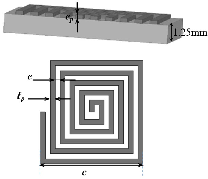
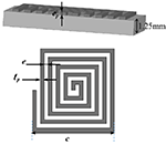
The proposed sensor consists, in fact, of a square flat coil, distributed over a total thickness of 1.25 mm. The length of the side is c = 2.6 mm, the width of tracks = 100 m, and the thickness e = 25 m. The coil features five turns distributed over its entire surface with a spacing of e = 100 m. Figure 1 shows a schematic view of the coil used in our application. This geometry gives the coil the highest inductance value and it is favorable in several points (Section III).
Figure 1: Schematic view of the sensor.
III. SENSOR CHARACTERIZATION
A. Geometrical characterization
It is interesting for the characterization to calculate the two geometrical quantities, which are the developed length of the wire and the effective total surface. The developed length or the total wire length can be calculated by the following formula:
| (1) |
The total effective surface , which is the equivalent surface of all the turns, is given by
| (2) |
where is the external rib of the coil, is the inter-line distance, is the line width, and is the number of turns (see Figure 1).
B. Electrical characterization
The theoretical model of a coil (Figure 2) is an RLC dipole whose impedance is written as
| (3) |
with being the current/voltage pulsation, , and are, respectively, the inductance, the resistance, and the capacity of the induction coil. In standardized form, the impedance can be explained as
| (4) |
with being the quality factor and the resonant pulsation of the sensor.
The probe impedance with an excited current I at a frequency f which is our parameter of interest can be computed by using the FE modeling developed in Section IV.
Figure 2: Electrical model of the coil.
The inductance of the probe is obtained by the following expression:
| (5) |
where is the coil excitation current and is the average magnetic energy stored throughout the space defined by the following relation:
| (6) |
where b is the magnetic flux density and h is the magnetic field.
The resistance of the coil can be calculated from the power losses in the conductive medium
| (7) |
with
| (8) |
where j is the EC density and is the material conductivity.
The total capacitance is expressed as a function of the electrical energy stored in the simulated space and the total voltage
| (9) |
with
| (10) |
where is the electric permittivity, e is the electric field, and is the whole computation area (sensor and air box).
C. Sensitive element characterization
The sensitivity of a sensor is the ratio of the respective variations of the output quantity of the sensor and the measurand. In the case of a coil used as an EC sensor, a magnetic field is transformed into a voltage . The sensitivity at a frequency is written as
| (11) |
The effective noise voltage of a coil when it is not traversed by a current is written as
| (12) |
where T is the temperature, is the measuring frequency range, and is Boltzmann’s constant.
The effective value of the equivalent magnetic noise is the ratio of the effective noise voltage and the sensitivity
| (13) |
The emissive ability is the ratio of the emitted field and the current required for its emission. Its expression is obtained using that of the magnetic flux produced by an inductance element crossed by a current , which is written with assumed to be uniform over the entire effective area of the coil
The emissive ability is given by
| (14) |
D. Optimization of the coil
The values of the geometrical, electrical, and physical characteristics are summarized in Table 1. The miniaturization of the coils in the printed circuit board is favorable on several points: the sensitivity is very high and the noise is very low. In all cases, the level noise is lower than the noise generally provided by the instrumentation and is, therefore, not very disturbing. Also, the thermal noise calculation is carried out over a wide range of frequencies, and, therefore, it is very strongly overestimated. In addition, the resolution is significantly improved by the printed coils: indeed, it is roughly proportional to the footprint, which is very small for this technology. The emitting power is inversely proportional to the total effective area, which means that a solenoid coil will emit a weaker field at an equal current.
Table 1: Numerical values of the coil characteristics calculated at 800 kHz
| Parameter | Value | |
|---|---|---|
Geometrical characterization |
Number of turns External length Line width Inter-line width Developed length Total surface |
5 2.6 m 100 m 100 m 36 mm 17.8 mm |
| Electrical characterization | Capacity C Resistance R Inductance L Resonant frequency f |
79.65 f F 0.028 0.023 m 1.98 MHz |
| Sensitive element | Sensitivity S Noise voltage v Equivalent noise field B Emissive ability P |
89.42 V/T 0.214 V 1.29 mT/A |
IV. MODELING
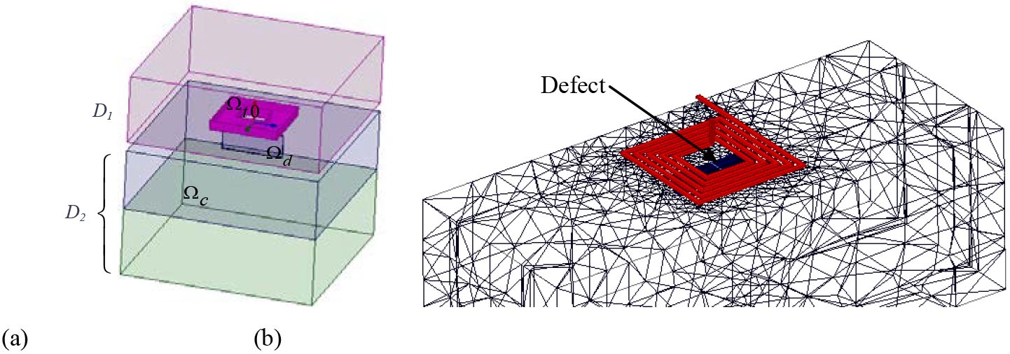
The test case is related to Eddy current nondestructive testing (ECT). It consists of a printed coil placed above a conductive plate. The inspected specimen is a nickel-based alloy affected by a rectangular defect (flaw). The parameters of the configuration are given in Table 2. The following figure shows the geometry of the considered problem. It is composed of two domains where the first one, , contains a coil, , where a uniform current density is imposed, and the second one, , contains a nickel alloy plate noted by which includes the flaw . These domains are separated by a meshed region called the lift-off.
The FEM program was written using the developed ANSYS program with conjunction with Matlab. The calculation is carried out in the context of harmonic quasi-stationary regime.
Figure 3: (a) Description of the studied problem. (b) 3D mesh of the geometry.
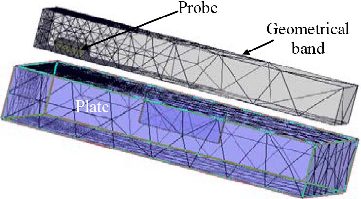
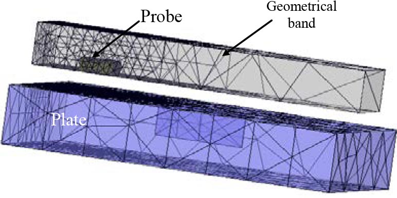
The displacement of the sensor along the conductive plate is formed using the motion band method defined from the extension of the 2D FEM. Figures 4 and 5 show the scheme illustrating this technique. It consists of two steps.
Create a geometrical band, during which the moving zone is subdivided into elementary regions of the identical length. Then the geometry is all meshed.
Figure 4: Moving band technique for sensor displacement: before probe displacement.
Locate in the geometrical band (moving zone) the regions corresponding to the sensor and the air, and then the physical properties of the sensor and the air are assigned at each step displacement.
Figure 5: Moving band technique for sensor displacement: after probe displacement.
V. DUAL FORMULATIONS FOR EDDY CURRENT PROBLEMS
Most three-dimensional finite element formulations of EC problems can be classified into two dual formulations. One works with the variables of the Ampere’s law system, and the other uses the variables of the Faraday’s law system. We will be interested in the two electric and magnetic formulations in combined potentials.
A. Magnetic formulation
The magnetic field h is then expressed by the sum of electric potential vectors t and , and the gradient of the magnetic scalar potential
| (15) |
such as and , with j and being the density of ECs and the density of current source. By introducing these equalities into the Faraday law and the flow conservation law, the system to solve is written as
| (16) |
with being the current/voltage pulsation, the relative permeability of the material used as inductor. The electric vector potential t and the magnetic scalar potential in an element are then expressed by
| (17) |
| (18) |
where is the vector of nodal shape functions, is the value of at the n node, is the vector of edge shape functions, and is the circulation of t along the edge. The matrix form of the system of equation is written as follows:
| (19) |
The system thus obtained is symmetrical and the matrix terms are
| (20) |
where is the stiffness matrix of the nodes, is the stiffness matrix of the edges, is the mass matrix of the edges, is the node-edge coupling matrix, and S is the source term.
The vectors and contain the unknowns of the system which are, respectively, the values of the magnetic scalar potential at the nodes and the circulations of the electric vector potential along the edges of themesh.
B. Electric formulation
The electric field e can be expressed by the combination of the magnetic vector potential a and electric scalar potential
| (21) |
The conduction current density j is thus calculated as
| (22) |
Following the same procedure as for formulation: The magnetic vector potential a and the electric scalar potential are then expressed by
| (23) |
| (24) |
In the same way as the formulation, the magnetic vector potential a is discretized by edge elements, while the electric scalar potential is discretized by nodal elements. The system of equations is written within the matrix form
| (25) |
The system thus obtained is symmetrical and the matrix terms are
| (26) |
The vectors and are the unknowns of the system, respectively, the values of the electric scalar potential at the nodes and the circulations of the magnetic vector potential at the edges of themesh.
Table 2: Dimensions of the problem
| Turn width | 100 m |
|---|---|
| Turn thickness | 25 m |
| Gap between turns | 100 m |
| Plate thickness | 3 mm |
| Plate conductivity | 0,76 MS/m |
| Relative permeability of the plate | 1 |
| Lift-off thickness | 50 m |
| Excitation frequency | 800 kHz |
| Length of the flaw | 800 m |
| Width of the flaw | 100 m |
| Depth of the flaw | 400 m |
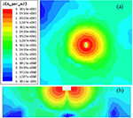
Figure 6: Eddy current distribution. (a) Top view. (b) Front view.
VI. APPLICATIONS
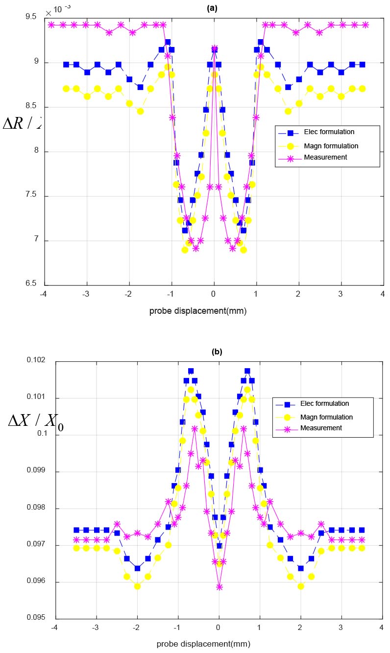
Our study relies on analyzing the data of scans, allotted by little displacements of the detector, parallel to the crack on the conductive plate. The change of the real and imaginary parts of the coil impedance reflects the change in the physical parameters of a test specimen in the presence of defects. The real part of the coil impedance is determined by calculating the Joule losses in the conductive media. The imaginary part of this impedance is determined from the magnetic energy stored in the entire meshed space.
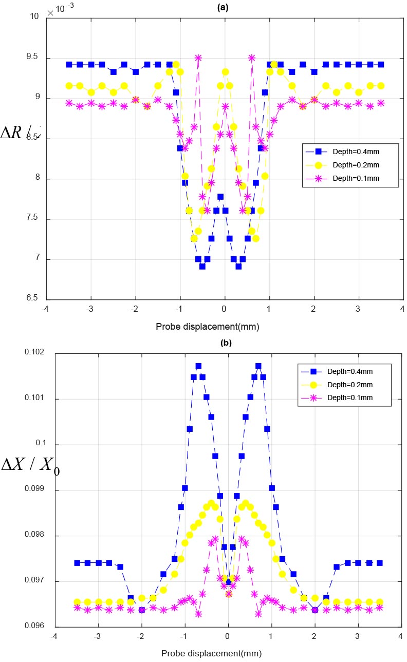
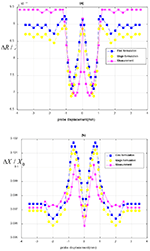
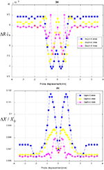
Figure 7: The variation of normalized impedance of the system as a function of displacement of the sensor. (a) Impedance real part. (b) Impedance imaginary part.
For both dual formulations, the variations of the real part and the variation of the imaginary part of the impedance due to the flaw are calculated by subtracting for each of them the values with and without flaw. and with being the reactance and resistance of the coil in presence of the conducting domain. are the reactance and resistance of the empty coil (absence of the plate).
A. Application I
The parameters of the configuration are given inTable 2.
Figure 6 illustrates the distribution of ECs produced by the coil. As can be seen in Figure 6(a), a circular-shaped EC loop is produced beneath the surface of the material. The current density is null in the defect zone because the conductivity is zero (), and it is also very significant in the surface and it decreases gradually as we head to the bottom because of the skin effect as shown in Figure 6(b).
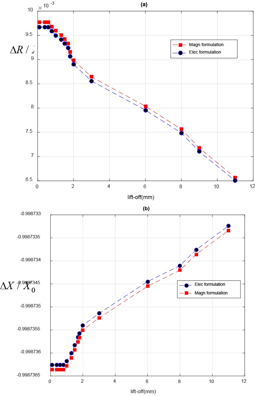
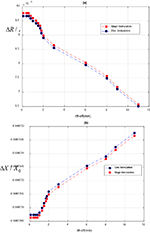
Figure 8: (a) Normalized resistance. (b) Normalized reactance variation as a function of the lift-off.
Figure 7(a) and (b) presents the variation of resistance and reactance as a function of the position of the symmetry axis of the coil relatively to the center of the flaw. The impedance real part (resistance) presents a trough curve and the imaginary part (reactance) presents a crest curve. As seen from the defect response curve of the impedance imaginary part [Figure 7(b)], the defect response begins to rise when the crack is near to the bottom edge of the coil, and it reaches a climax when the sensor coincides with the first edge of the defect and starts to decrease as the sensor leaves the other edge of the defect. It can be observed from the next figures that there is a good agreement between the FEM results issued from the magnetic and the electric formulation and the experimental results. These signals represent the signatures of the crack.
B. Application II
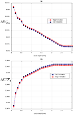
As the lift-off is a predominant factor in the EC detection performance, the modeling must take into account the physical phenomena associated with its values. The geometrical and physical parameters of the problem are summarized in Table 2. The lift-off varies within a range of 0.111 mm. the resistance and reactance of the coil were calculated with both the electrical and magnetic formulations and shown in Figure 8(a) and (b). The results presented in these figures show that the influence on the coil impedance of a lift-off less than 1 mm is negligible. Indeed, for a lift-off of less than 1 mm, the reactance and the resistance of the coil are almost constant. On the other hand, beyond this value, the lift-off has a strong influence on the impedance, and it is essential to take this into account in the modeling. The results also show that the two curves obtained by the two electric and magnetic formulations are in good agreement. This value (1 mm) depends on the coil used. In a general way, an increase in the size of the coil will lead to an increase in thesevalues.
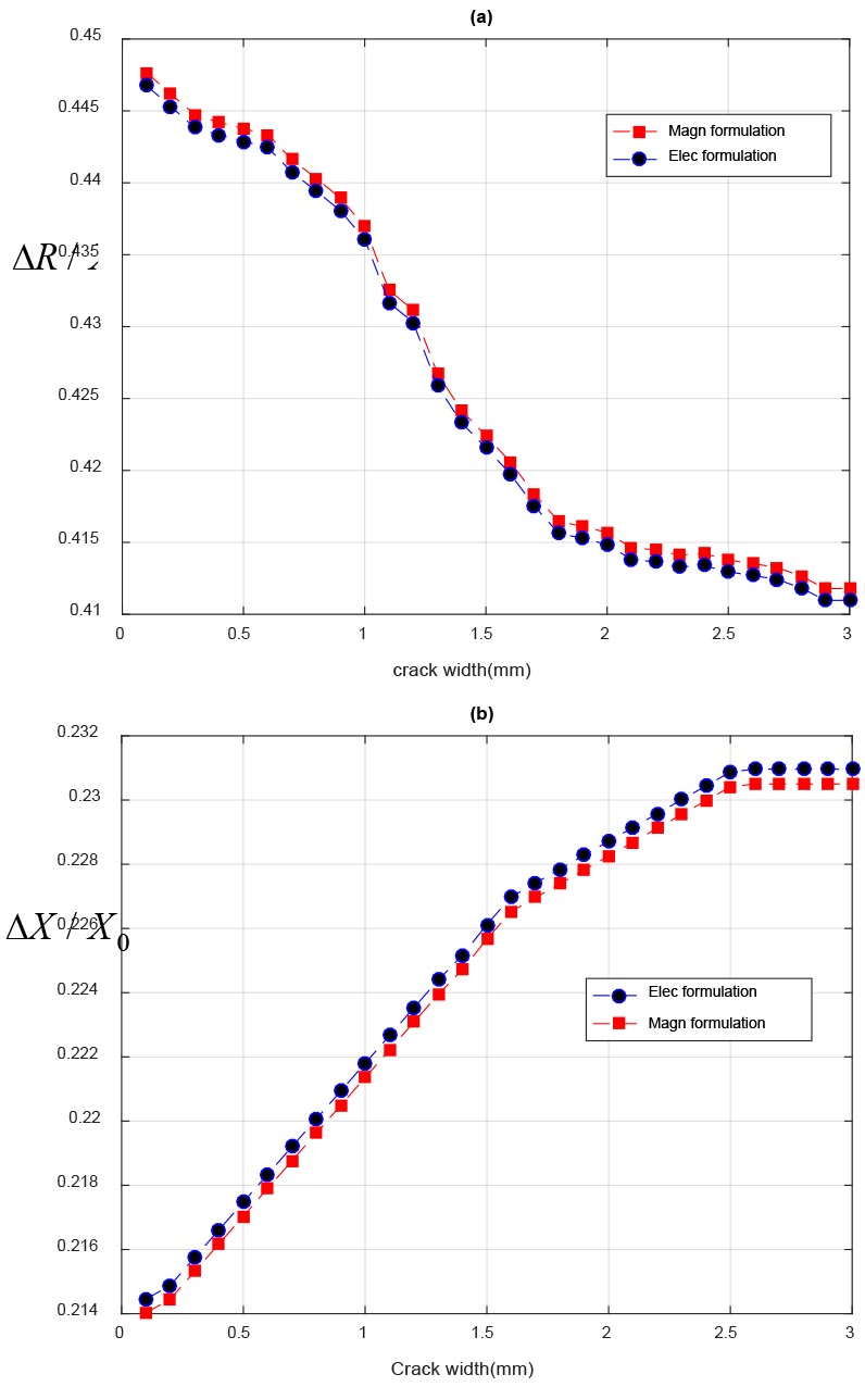
Figure 9: (a) Normalized impedance real part. (b) Normalized impedance imaginary part variation as a function of the crack width.
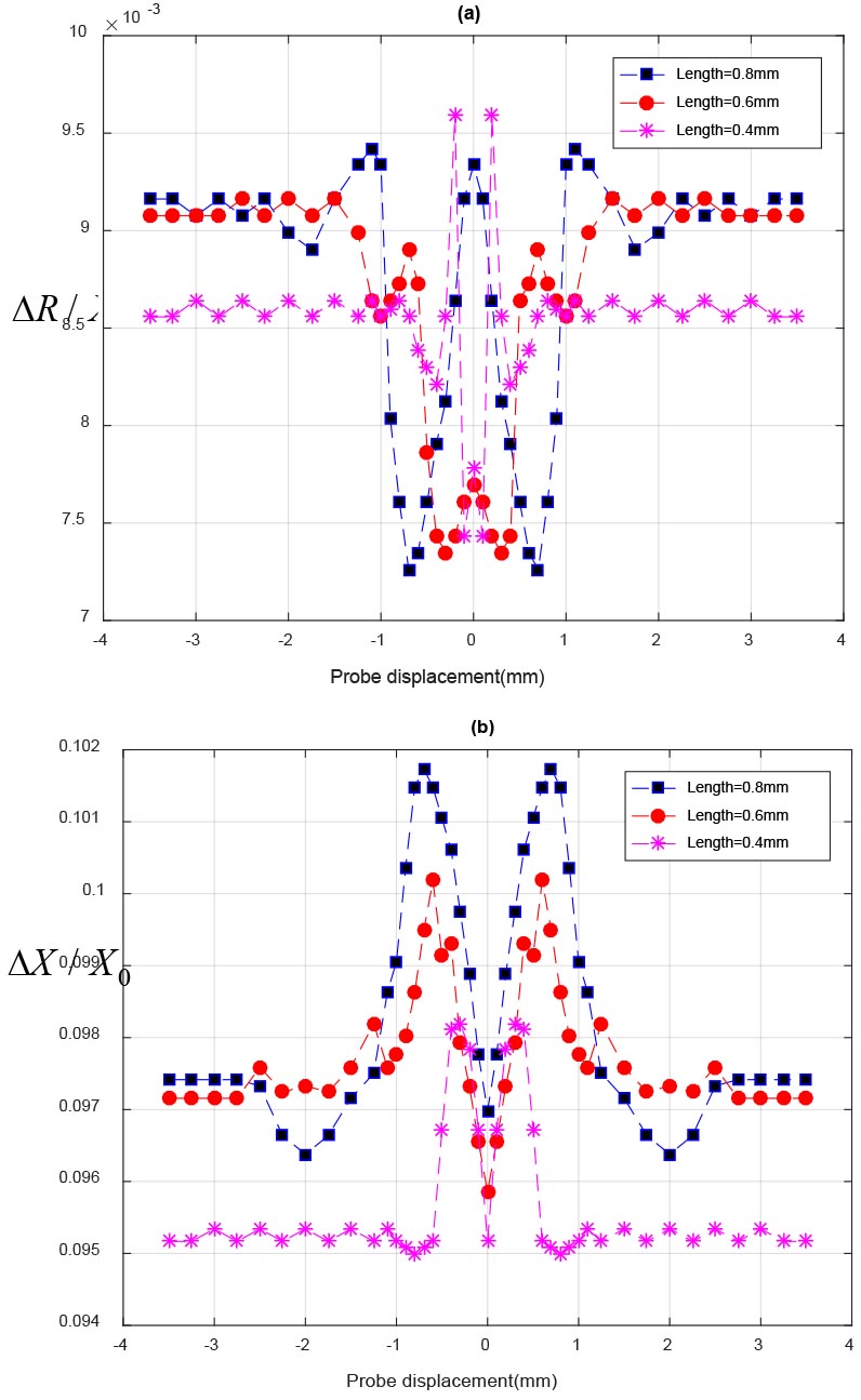
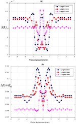
Figure 10: (a) Normalized impedance real part. (b) Normalized impedance imaginary part variation of cracks having different lengths.
Figure 11: (a) Normalized impedance real part. (b) Normalized impedance imaginary part variation of cracks having different depths.
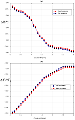
Figure 12: (a) Normalized impedance real part. (b) Normalized impedance imaginary part variation as a function of the crack depth.
C. Application III
The study of the crack size effect on the ECsignal will enable us to identify the ECNDT device sensitivity.
Effect analysis of crack width:
In the previous works, the authors were more interested in studying the effect of the length and depth of the crack on the EC signal, while only a few of them were interested in studying the width effect.
The model used is the same one used for application I by changing the geometric parameters of the defect. The frequency of the sensor is fixed at 0.8 MHz and the lift-off at 0.0625 mm (application II), and the length of the plate is much greater than that of the crack, the crack length and depth are fixed at 0.8 and 0.4 mm, respectively, while the width is varying between 0.1 and 3 mm for a step of 0.1 mm. In this case, we fix the crack beneath the center of the sensor where its output is in the maximum. The graphs of the impedance real part and imaginary part versus crack width are shown in Figure 9(a) and (b), respectively.
Effect analysis of crack length:
Next the influence of crack length on the sensor response is studied. The lift-off is set to be 0.0625 mm, and cracks of identical width (0.1 mm) and depth (0.4 mm) having different lengths are altered. Data of scans are carried out by small displacements of the sensor with a step of 0.1 mm, parallel to the crack on the surface of the material. Figure 10(a) and (b) presents EC signatures of the resistance and reactance variations with respect to the sensor displacement produced by cracks having different lengths. Based on the curves of impedance real part and imaginary part, the shapes of the curves for all the defects are similar; however, the defect length influences the width and the peak value of the response curve. As the crack length grows, the width of the curve grows and the peak valueincreases.
Effect analysis of crack depth:
Defects with depths of 0.1, 0.2, and 0.4 mm are studied. All the defects are 0.8 mm in length and 0.1 mm in width. Figure 11(a) and (b) shows EC signatures of the impedance real part and imaginary part variations with respect to the sensor displacement produced by defects having different depths. As can be seen, the waveforms are similar; however, the crack depth influences the peak value of the response curves. The deeper the crack is, the greater the peak will be.
EC signal and the depth limit:
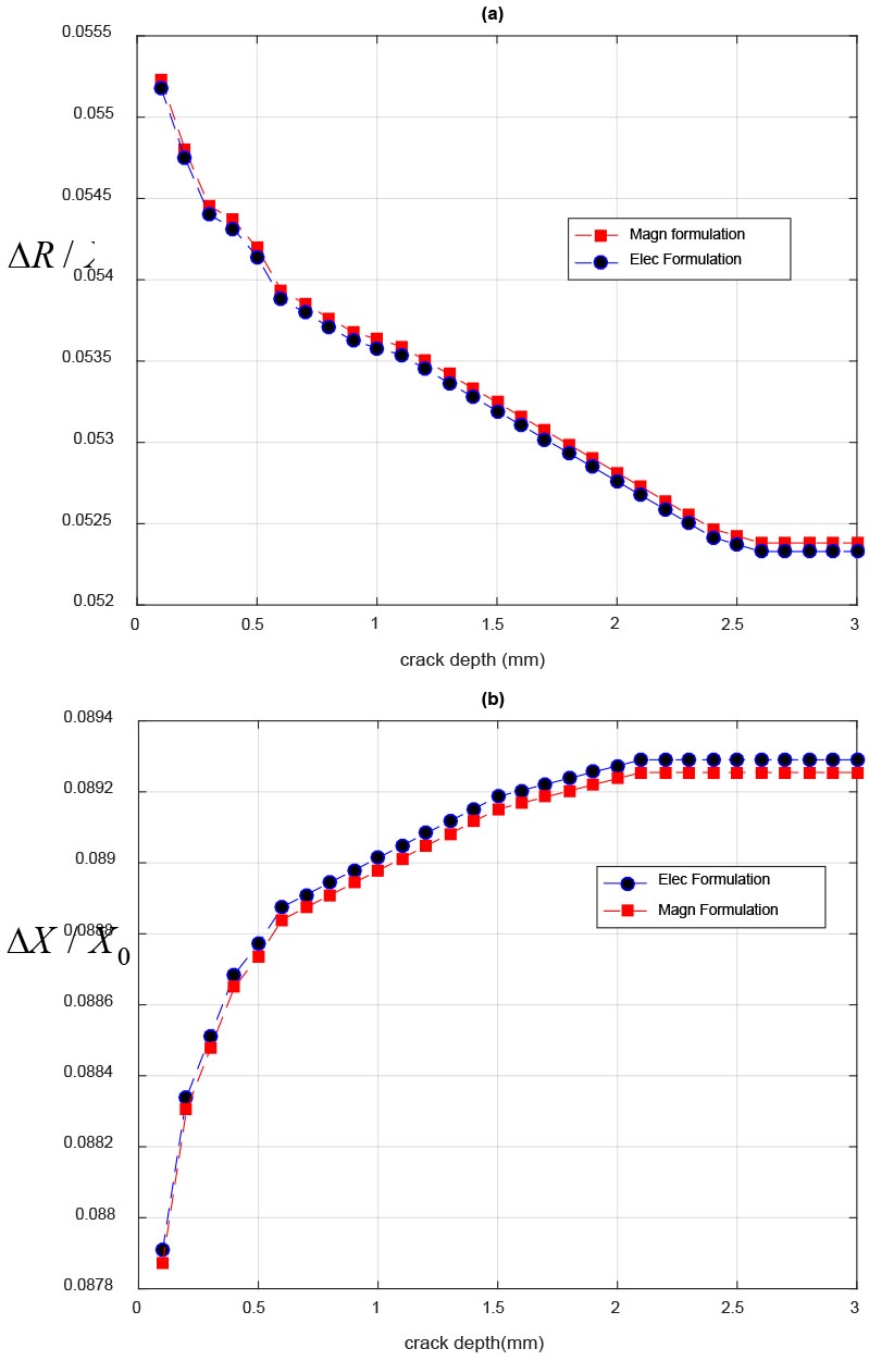
Next, the depth limit is studied; the crack length and width are fixed at 0.8 and 0.1 mm, respectively, while the depth is varying between 0.1 and 3 mm for a step of 0.1 mm. In this case, we fix the crack beneath the center of the sensor where its output is in the maximum. The graph of the impedance real part and imaginary part versus crack depth are shown in Figure 12(a) and (b), respectively.
As can be seen, at the beginning, the resistance values decrease rapidly, then slow down gradually with increasing crack depth, and then stabilize when the crack depth reaches 2.5 mm. On the other hand, the reactance values increase rapidly at the beginning and slow down gradually, while the crack depth increases and then stabilizes when the crack depth reaches 2 mm. The reason is that when we use a high frequency excitation, the EC will be spread out much more on the surface of the material so that the sensor will not be very sensitive to deep defects as it is with the shallow defects. Both Figures 12(a) and (b) show that the depth limit is not the same for the impedance real part and imaginary part. The real part is more sensitive to the crack depth than the imaginary part.
VII. CONCLUSION
A microsensor dedicated to the ECNDT application is proposed in this paper. An FEM approach that yields an efficiency to model the 3D microsensor, taking into account the presence of thin geometrical domains and the sensor displacement in the 3D plane without remeshing all the domains in each displacement, has been proposed. The real and imaginary parts of the impedance at every position of the sensor computed by experiments and simulations were consistent with each other for the first application. The optimal lift-off, which is less than 1 mm, is determined by FEM simulation in the second application and taken into account in all the applications (I and III). The principle of the sensor and the response of cracks with different sizes are demonstrated by simulation, and the results are very close because both the proposed differential formulations (in terms of the magnetic formulation and the electric formulation) can deal with currents flowing in conductors and are well fitted for computing fields within the current regions with accuracy. The difference between the impedance values obtained using the magnetic formulation and the electric formulation did not exceed, in any case, 0.1%. The novel sensor has the followingadvantages:
The design of the sensor conforms it to the small geometry.
It provides high spatial resolution and high detection efficiency.
The sensor was capable of detecting micro-defects with a size starting from 0.1 mm under the optimal excitation frequency of 0.8 MHz.
The sensor can distinguish the different crack sizes (length, width, and depth).
Future research will be required to extend the proposed sensor for solving problems with complex geometry and arbitrary defect.
REFERENCES
[1] Q. Yu, O. Obeidat, and X. Han, “Ultrasound wave excitation in thermal NDE for defect detection,” NDT E Int., vol. 100, pp. 153‑165, Sept. 2018.
[2] O. Obeidat, Q. Yu, L. Favro, and X. Han, “The effect of heating duration on the quantitative estimation of defect depth using sonic infrared imaging,” J. Nondestruct. Eval. Diagn. Progn. Eng. Syst., vol. 4, no. 4, pp. 302‑307, Nov. 2021.
[3] D. Velicheti, P. B. Nagy, and W. Hassan, “Residual stress and cold work assessment in shot-peened IN718 using a dual-mode electromagnetic technique,” NDT E Int., vol. 121, May 2021.
[4] D. Velicheti, P. B. Nagy, and W. Hassan, “Inversion procedure for dual-mode electromagnetic nondestructive characterization of shot-peened IN718,” NDT E Int., vol. 101, pp. 17‑28, Oct.2019.
[5] K. Li and al., “A fast and non-destructive method to evaluate yield strength of cold-rolled steel via incremental permeability,” J. Magn. Magn. Mater., vol. 498, Nov. 2020.
[6] A. Goti, A. Oyarbide-Zubillaga, A. Sanchez, T. Akyazi, and E. Alberdi, “Multi equipment condition based maintenance optimization using multi-objective evolutionary algorithms,” Appl. Sci. Switz., vol. 9, no. 22, Nov. 2019.
[7] M. Alsharqawi, T. Zayed, and S. Abu Dabous, “Integrated condition-based rating model for sustainable bridge management,” J. Perform. Constr. Facil., vol. 34, no. 5, Jun. 2020.
[8] R. M. Ayo-Imoru and A. C. Cilliers, “A survey of the state of condition-based maintenance (CBM) in the nuclear power industry,” Ann. Nucl. Energy, vol. 112, pp. 177‑188, Feb. 2018.
[9] M. M. Derriso, C. D. McCurry, and C. M. Schubert Kabban, “2 - A novel approach for implementing structural health monitoring systems for aerospace structures,” in Structural Health Monitoring (SHM) in Aerospace Structures, F.-G. Yuan, Éd. Woodhead Publishing, pp. 33‑56, Oct. 2016.
[10] M. Lu, X. Meng, L. Chen, R. Huang, W. Yin, and A. Peyton, “Measurement of ferromagnetic slabs permeability based on a novel planar triple-coil sensor,” IEEE Sens. J., vol. 20, no. 6, pp. 2904‑2910, March 2020.
[11] Y. Long, S. Huang, Y. Zheng, S. Wang, and W. Zhao, “A method using magnetic eddy current testing for distinguishing ID and OD defects of pipelines under saturation magnetization,” Applied Computational Electromagnetic Society (ACES) Journal, pp. 1089‑1098, Sept. 2020.
[12] X. Chen and Y. Lei,“Electrical conductivity measurement of ferromagnetic metallic materials using pulsed eddy current method,” NDT E Int., vol. 75, pp. 33‑38, Oct. 2015.
[13] B. Helifa, M. Feliachi, I. K. Lefkaier, F. Boubenider, A. Zaoui, and N. Lagraa, “Characterization of surface cracks using eddy current NDT simulation by 3D-FEM and inversion by neural network,” Applied Computational Electromagnetic Society (ACES) Journal, pp. 187‑194, Feb. 2016.
[14] F. Jiang, S. Liu, and L. Tao, “Quantitative research on cracks in pipe based on magnetic field response method of eddy current testing,” Applied Computational Electromagnetic Society (ACES) Journal, pp. 99‑107, Jan. 2021.
[15] J. O. Fava, L. Lanzani, and M. C. Ruch, “Multilayer planar rectangular coils for eddy current testing: Design considerations,” NDT E Int., vol. 42, no. 8, pp. 713‑720, Dec. 2009.
[16] M. A. Machado, K.-N. Antin, L. S. Rosado, P. Vilaça, and T. G. Santos, “Contactless high-speed eddy current inspection of unidirectional carbon fiber reinforced polymer,” Compos. Part B Eng., vol. 168, pp. 226‑235, July 2019.
[17] H. Zhang, L. Ma, and F. Xie, “A method of steel ball surface quality inspection based on flexible arrayed eddy current sensor,” Measurement, vol. 144, pp. 192‑202, Oct. 2019.
[18] N. Zhang, C. Ye, L. Peng, and Y. Tao, “Eddy current probe with three-phase excitation and integrated array tunnel magnetoresistance sensors,” IEEE Trans. Ind. Electron., vol. 68, no. 6, pp. 5325‑5336, April 2021.
[19] Z. Sun, D. Cai, C. Zou, W. Zhang, and Q. Chen, “Design and optimization of a flexible arrayed eddy current sensor,” Meas. Sci. Technol., vol. 28, no. 4, Feb. 2017.
[20] W. Zhang, C. Wang, F. Xie, and H. Zhang, “Defect imaging curved surface based on flexible eddy current array sensor,” Measurement, vol. 151, Feb. 2020.
[21] J. Ge, B. Hu, and C. Yang, “Bobbin pulsed eddy current array probe for detection and classification of defects in nonferromagnetic tubes,” Sens. Actuators Phys., vol. 317, Jan. 2021.
[22] S. Xie, Z. Duan, J. Li, Z. Tong, M. Tian, and Z. Chen, “A novel magnetic force transmission eddy current array probe and its application for nondestructive testing of defects in pipeline structures,” Sens. Actuators Phys., vol. 309, July. 2020.
[23] M. Lu, X. Meng, R. Huang, L. Chen, A. Peyton, and W. Yin, “Lift-off invariant inductance of steels in multi-frequency eddy-current testing,” NDT E Int., vol. 121, April 2021.
[24] Z. A. Ansari, B. A. Abu-Nabah, M. Alkhader, and A. Muhammed, “Experimental evaluation of nonmagnetic metal clad thicknesses over nonmagnetic metals using apparent eddy current conductivity spectroscopy,” Meas. J. Int. Meas. Confed., vol. 164, June 2020.
[25] N. M. Rodrigues, L. S. Rosado, and P. M. Ramos, “A portable embedded contactless system for the measurement of metallic material conductivity and lift-off,” Measurement, vol. 111, pp. 441‑450, Dec. 2017.
[26] S. Zhang, “An analytical model of a new T-cored coil used for Eddy current nondestructive evaluation,” Applied Computational Electromagnetic Society (ACES) Journal, pp. 1099‑1104, Sept. 2020.
[27] S. da Silva, “Data-driven model identification of guided wave propagation in composite structures,” J. Braz. Soc. Mech. Sci. Eng., vol. 40, no. 11, Oct. 2018.
[28] F. Jiang and S. Liu, “Calculation and analysis of an analytical model for magnetic field monitoring based on TREE in Eddy current testing,” Applied Computational Electromagnetic Society (ACES) Journal, pp. 1489‑1497, Dec. 2018.
[29] O. Obeidat, Q. Yu, and X. Han, “Developing algorithms to improve defect extraction and suppressing undesired heat patterns in sonic IR images,” Sens. Imaging, vol. 17, no. 1, Oct.2016.
[30] G. Tytko and L. Dziczkowski, “Fast calculation of the filamentary coil impedance using the truncated region eigenfunction expansion method,” Applied Computational Electromagnetic Society (ACES) Journal, pp. 1461‑1466, Dec. 2018.
[31] M. Haywood-Alexander, N. Dervilis, K. Worden, E. J. Cross, R. S. Mills, and T. J. Rogers, “Structured machine learning tools for modelling characteristics of guided waves,” Mech. Syst. Signal Process., vol. 156, July 2021.
[32] K. Mizukami and Y. Watanabe, “A simple inverse analysis method for eddy current-based measurement of through-thickness conductivity of carbon fiber composites,” Polym. Test., vol. 69, pp. 320‑324, Aug. 2018.
[33] M. Mirzaei, P. Ripka, A. Chirtsov, and V. Grim, “Eddy current speed sensor with magnetic shielding,” J. Magn. Magn. Mater., vol. 502, May2020.
[34] K. Mizukami et al., “Enhancement of sensitivity to delamination in eddy current testing of carbon fiber composites by varying probe geometry,” Compos. Struct., vol. 226, Oct. 2019.
[35] C. Ye, Y. Wang, M. Wang, L. Udpa, and S. S. Udpa, “Frequency domain analysis of magnetic field images obtained using TMR array sensors for subsurface defect detection and quantification,” NDT E Int., vol. 116, Dec. 2020.
[36] Y. Kuang et al., “Magnetic field energy harvesting from the traction return current in rail tracks,” Appl. Energy, vol. 292, June 2021.
[37] S. She, Y. Chen, Y. He, Z. zhou, and X. Zou, “Optimal design of remote field eddy current testing probe for ferromagnetic pipeline inspection,” Measurement, vol. 168, Jan. 2021.
BIOGRAPHIES

Chifaa Aber received the magister degree in applied optics from the University of Ferhat Abbas Setif, Sétif, Algeria, in 2010. She is currently working toward the Ph.D. degree with the University of Sciences and Technologies of Oran USTO-MB.
She is a member of Applied Power Electronics Laboratory LEPA and temporary teacher with Larbi Ben M’hidi OEB University. Her research interests include Eddy current, microelectronics, neural network, FEM, and optical sensors.

Azzedine Hamid was born in Algies, Algeria, in 1961. He received the magister degree in electrical engineering from the Mohamed Boudiaf University of Oran in 1994 and the Ph.D. degree from the Mohamed Boudiaf University of Sciences and Technology of Oran in 2005.
He is a head member of LEPA laboratory research team.

Mokhtar Elchikh received the Ph.D. degree in nuclear and particle physics from the University of Grenoble I, Grenoble, France, in 1992.
His is currently a Professor of Physics with the University of Sciences and Technology of Oran, Algeria. He has been interested in nuclear physics, spin physics, ion-surface interactions, condensed matter physics, ab initio calculations, and, recently, in power electronic.

Thierry Lebey received the M.Sc. degree in solid state physics in 1984 and in microelectronics in 1985, and the Ph.D. degree in electrical engineering in 1989. He was a CNRS Research Scientist for 30 years. His fields of interest concern the characterization, modeling, and aging of solid dielectrics and insulating materials used in electrical engineering applications. From 2016 to 2019, he was the Director of LAPLACE, the French largest electrical engineering laboratory located in Toulouse, France. Since then, he joined SafranTech, the corporate research center of Safran, one of the first world aerospace companies, as the head of research on high voltage engineering for aviation applications. He is the author of around 90 papers in international journals AND more than 160 conference papers (mainly in IEEE conferences) and holds 18 international patents. https://www.safran-group.com/
ACES JOURNAL, Vol. 37, No. 1, 117–128.
doi: 10.13052/2022.ACES.J.370114
© 2021 River Publishers
