PET-Based Instant Inkjet-Printed 4 4 Butler Matrix Beamforming Network
Suleiman A. Babale, Sharul Kamal A. Rahim, Kim G. Tan, Kashif N. Paracha, Arslan D. Butt, Irfan Ali, and S. H. Lawan
1Department of Electrical Engineering, Bayero University Kano, Kano 3011, Nigeria
sababale.ele@buk.edu.ng, shlawan.ele@buk.edu.ng
2Wireless Communication Centre, Universiti Teknologi Malaysia (UTM), Johor Bahru 81310, Malaysia
sharulkamal@fke.utm.my, irfan_lrk_15@yahoo.com
3Faculty of Engineering & Technology, Multimedia University, Jalan Ayer Keroh Lama, Melaka 75450, Malaysia
kgtan@mmu.edu.my
4Department of Electrical Engineering, Government College University, Faisalabad 38000, Pakistan
kashifnisar@gcuf.edu.pk, arslandawood@gcuf.edu.pk
Submitted On: January 26, 2021; Accepted On: November 20, 2021
Abstract
In this paper, a novel planar Butler matrix (BM) utilizing only hybrid couplers and a crossover are implemented using a low-cost silver-nano inkjet printing technique. Unlike in the conventional design of BM where a phase shifter is required, this novel design does not need a phase shifter to be implemented. However, the use of delicate substrates like polyethylene terephthalate (PET) in the design makes it unique. This is not possible with the conventional thermal curing process, as PET substrate cannot be subjected to an excessively feverish temperature. The results obtained show good return loss and transmission coefficients better than and , respectively, at the center frequency. Similarly, an amplitude imbalance of less than with phase mismatch within is achieved at the center frequency. The BM has a bandwidth of 24.79% with a beam pattern produced at ,, , and when ports 1-4 of the BM are energized.
Keywords: Modified coupler, PET substrate, Butler matrix, crossover.
I. INTRODUCTION
Previously, base-station uses an omnidirectional antenna for communications. The use of this type of antenna serves as a waste of power since most of the power radiates in all directions, instead of being directed toward the desired user. Moreover, sometimes, this radiated energy also served as an interferer to the nearby cells. With the advent of smart antenna technology (SAT), this problem was drastically minimized. Antenna beamforming network is generally known as an adaptive antenna array as per IEEE Standard. It is a type of antenna system that consists of external circuitries and radiating elements whose properties are controlled by the signal being received [1]. There are broadly two types of antenna beamforming network: the switched beam system (SBS) with fixed beam and variable phases and the adaptive antenna array with variable amplitude and phase [2]. Butler matrix (BM) falls under the category of SBS. BM is among the well-known beamforming networks because of its structural simplicity, compactness, cost-effectiveness, and easy fabrication. It is being made from hybrid couplers [3], crossing lines, and some phase delays [4-6]. It is a vital component of most array-based multiple-inputs multiple-outputs (MIMO) antenna systems. Its beam scanning is important in increasing the channel capacity of a system and reduces interference [7]. Planar BMs were reported in different technologies, such as in substrate integrated waveguides [8], [9], inkjet printing technique [10], multi-layered techniques [11, 12], composite right-left handed transmission line (CRLH TL) [13], swapped-port couplers [14], and suspended stripline technology [15]. In [16], [17], BM beamforming network was designed by integrating additional controllers and phase shifters to control the beam steering array. But the bandwidths are mostly less than 15% due to the requirement of the couplers involved [18]. To maintain the phase difference at the intermediate and the final stages of the design, hybrid couplers together with phase shifters are used [19]. These phase shifters sometimes contributed in deterring good performances of BM due to introduction of losses [20] and untolerable phase ripples [21]. BM without crossover was presented in [22]. But the patch used in the coupler has complex nature and its field distribution does not have a closed-form equation that characterized its geometry using any well-known transmission line (TL) theory. However, the ground plane pattern, some of its variables, and their locations can only be obtained using time-consuming and complex processes. The BM presented in [23] does not use a phase shifter, but a via is needed for crossing the signals. Despite the importance of couplers in many designs like BM, little has been done on arbitrary output phase-difference characteristics [24], [25]. In [25], a hybrid coupler with arbitrary phase-difference was proposed. But, the method has some drawbacks and was corrected in [26]. This idea was conceived in this paper to propose an inkjet-printed BM.
In this paper, a novel 4 4 BM utilizing modified couplers and a crossover are presented. Using couplers with phase difference in this design eliminates the use of phase shifters, and this, in turn, reduces the dimension and TL losses of the device by shortening the TL path. We demonstrated the BM by prototyping using instant inkjet printing technology that does not require thermal curing. One advantage of this printing process is the use of chemical sintering which paves a way for seamless and fast prototyping of electronic devices using delicate types of substrate materials. For example, the use of paper and polyethylene terephthalate (PET) substrates is not possible with the thermal curing process as they cannot be subjected to an excessively feverish temperature.
II. THE INKJET PRINTING TECHNIQUE
The technique presented in this paper uses a chemical sintering process based on conductive silver nanoparticles ink utilizing an inkjet printer by Brother Industries, Ltd. (model: DCP–J140w). The choice of this type of printer is because of its low cost and availability as compared to other chemical sintering processes [10], [27]. Another advantage of this type of printer is the effectiveness of its nozzles, which eject a moderate amount of ink volume at a given time which translates to deposition of the conductive ink in a manner that provides an undistorted conductive path [28]. Unlike other printing techniques that require thermal curing for a conductive pattern to be formed. Immediately after printing with this setup, the ink dried up and a conductive pattern is formed with a very low resistance of about within a few seconds.
Before evaluating a complex structure with this technique, a uniform TL of 50 cm length having an impedance of 50 was simulated using the properties of the silver-nano conductor as presented in [29]. Figure 1

Figure 1: (a) The Brother printer DCP–J140w, (b) layout and photograph of a 50- microstrip TL simulated and prototyped with the PET substrate, and (c) the S-parameters for the microstrip TL.
III. COUPLER DESIGN
To design any form of BM, the use of a coupler is inevitable. This section briefly describes the two types of couplers used in the implementation of theproposed BM.
A. Modified coupler
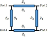
The concept used in the design of this novel 4 4 BM is centered on the design of hybrid coupler shown in Figure 2. This coupler is referred to as a modified coupler because its output phase difference is at as against the classical coupler whose output difference is .
Figure 2: Structure of the proposed coupler.
The design for the coupler has been adapted from [30] where the derivation for the design was not presented. However, the resulting equations used in our design of the coupler are shown here as eqn (1)–(5):
| (1) |
| (2) |
| (3) |
| (4) |
| (5) |
where, and are normalized with the reference impedance terminating the ports . The angles can be any arbitrary angle, is the power division ratio, and the phase difference at the center frequency is .
Using these coupler design equations, a 3-dB coupler with a phase difference of has been designed and simulated to operate at a frequency of 6 GHz. Using the designed equations, the phase difference between the outputs is set to be and the reference impedance is fixed at . Under these conditions, the impedances of the horizontal arm of the 3-dB coupler Z = 28.87 , whereas those of the horizontal arms are Z2 = Z3 = 35.36 , with , and . The use of this coupler having phase-difference eliminates the need for additional components in building the BM, thereby making it compact and retain its good performance. This is because it replaces the functions of both the quadrature coupler and phase shifter in the classical BM which gives a phase difference of either or at the output of the phase shifter. The physical parameters of the coupler are computed from the impedances and the electrical lengths of the coupler and are tabulated as shown in Table 1.
Table 1: Parameters of the modified coupler
| AL1 | 9.41 |
| AW1 | 0.93 |
| BL1 | 5.63 |
| BW1 | 1.08 |
| L1 | 1.41 |
| L2 | 3.67 |
| L3 | 2.82 |
| W | 1.08 |
| PL1 | 10.0 |
| PL2 | 3.67 |
| PL3 | 2.62 |
| PW1 | 0.67 |
The optimized parameters of each section of the modified coupler are indicated on the layout as shown in Figure 3(a). The simulated S-parameters showing the S-parameter response and the output phase difference are shown in Figure 3(b).

Figure 3: (a) Layout of the modified coupler. (b) S-parameter results of the modified coupler.
B. Classical coupler
The second type of coupler known as the classical coupler was also designed using eqn (1)-(5) outlined in the previous section. From these equations, setting the output phase difference to and the characteristics impedance of the line to , the corresponding impedances of the couplers’ vertical and horizontal arms become: and .
Table 2: Parameters of the classical coupler
| AL1 | 7.70 |
| AW1 | 1.10 |
| BL1 | 10.50 |
| BW | 0.68 |
| PL1 | 2.00 |
| PL2 | 3.52 |
| PL3 | 6.00 |
| PW1 | 0.67 |
The physical parameters of the coupler are computed from the impedances and the electrical lengths of the coupler and are tabulated as shown in Table 2. Also, the values of each section of the coupler are computed as indicated on the layout of Figure 4(a). Also, the S-parameters of the coupler are also shown in Figure 4(b).
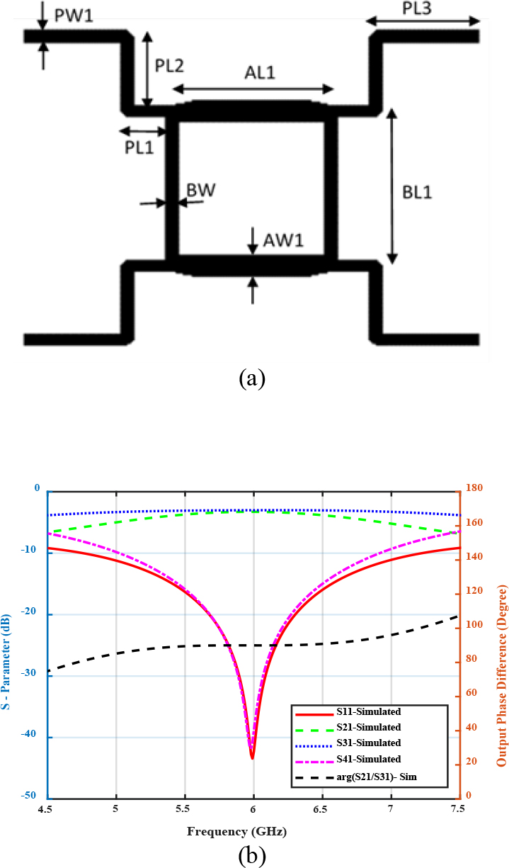
Figure 4: (a) Layout of the quadrature coupler. (b) S-parameter results of the coupler.
C. Microstrip crossover
The classical coupler designed was used to obtain the crossover used in the implementation of the BM. It was implemented by cascading the two 90 couplers designed in the previous section. But sometimes, the resulting structure has to be optimized for better results. Figure 5 (a) shows the schematic of the optimized crossover, while its S-parameter results are shown in Figure 5 (b).
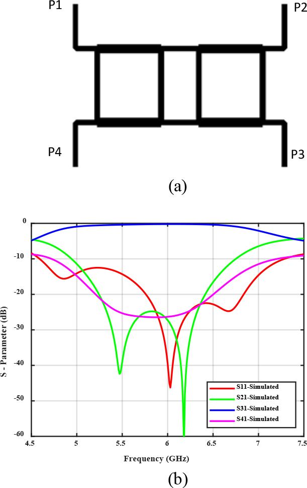
Figure 5: (a) Layout of the microstrip crossover. (b) S-parameter results of the crossover.
D. Patch antenna
A square-shaped microstrip patch antenna was designed based on the equations presented in [31], and the desired resonant frequency was set to 6 GHz to rhyme with that of the proposed BM. The design parameters of the single element microstrip patch antenna is calculated and presented in Table 3.
Table 3: Parameters of the patch antenna
| Substrate wavelength () | |
|---|---|
| Patch width () | |
| Patch length () | |
| Feed width () | |
| Substrate width () | |
| Substrate length () |
After obtaining the physical parameters of the single element patch antenna, a commercially available software, Computer Simulation Technology (CST), was used for the simulation. Figure 6 shows the geometry and radiation pattern of the single element patch antenna. From this figure, it can be seen that an excellent radiation pattern with a realized gain of , sidelobe level of and 3-dB angular beamwidth of has been obtained.
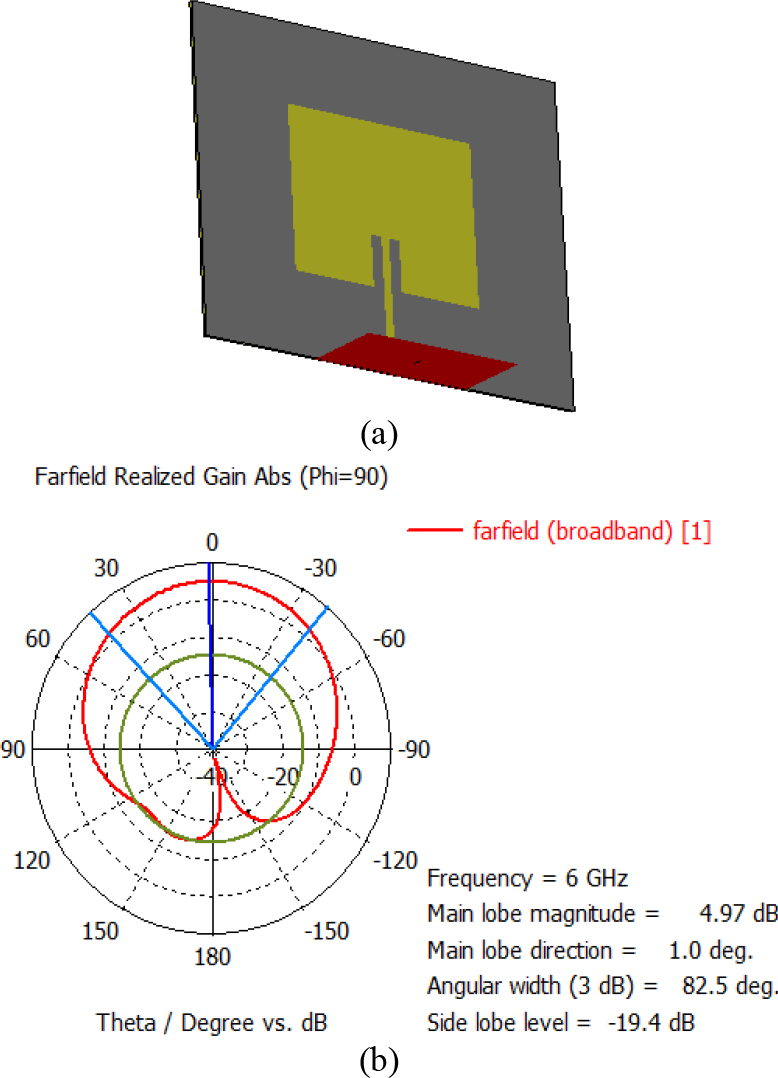
Figure 6: (a) Layout of the patch antenna. (b) S-parameter results of the patch antenna.
For quick verification, in practical design, the length L of a simple patch antenna is usually taken in the range of , where is the wavelength of the free-space. Also, the thickness of the patch which is typically the conductor thickness is usually taken such that . The height of the substrate is usually in the range of , and, finally, the dielectric constant of the substrate is typically in the range of [31].
IV. BUTLER MATRIX
The overall structure of the BM was obtained from the individual components designed in the previous sections. The BM was simulated and fabricated on the transparent PET substrate with a measured dielectric constant of 2.71, a thickness of 0.125 mm, and a loss tangent of 0.043. CST studio was used throughout the simulation and the silver-nano printing technology was used for the prototyping.
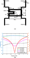
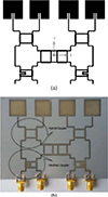
The layout and the photograph of the proposed BM feeding the antenna array are shown in Figure 7. It comprises the first two couplers, two conventional couplers, and a crossover. For ease of handling, the second crossover was eliminated in the design. This is because it only reverses the position of the signals at the output ports of the BM.
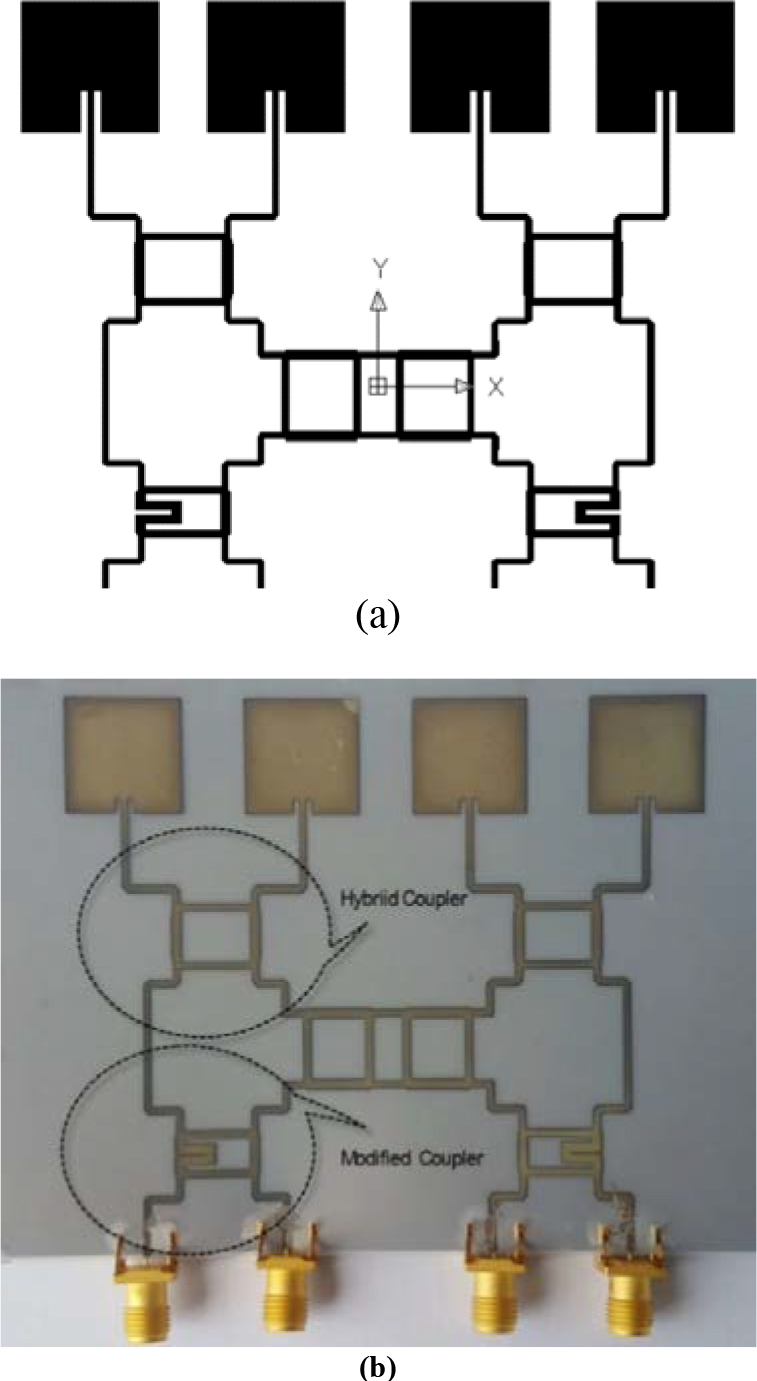
Figure 7: The proposed 4 4 Butler matrix. (a) Layout. (b) Photograph.
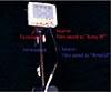
The fabricated BM was tested in an anechoic chamber to compare the radiation pattern produced as a result of exciting the BM. The experimental test stands for the measurements are shown in Figure 8.
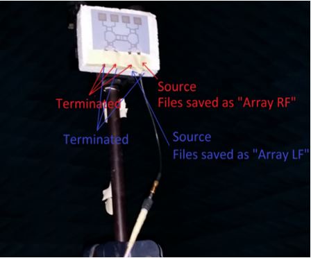
Figure 8: Experimental test stand for the complete BM and the antenna array.
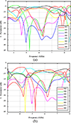
By exciting port 1 of the beamforming network, the return loss was found to be and the transmission characteristics are , , , and at the center frequency. Similarly, when a signal is applied at port 2 while terminating other ports with load, a return loss of and transmission coefficients of , , , and are obtained at the center frequency. Exciting ports 3 and 4 of the BM produces the same results as in ports 1 and 2. This is due to the symmetry of the beamforming network. In all the cases, the return losses are far below the line, and the transmission coefficient results approach the theoretical value of in each case with a maximum variation of less than . Figure 9(a) shows the return loss and isolation while the results of the transmission coefficients are shown in Figure 9(b). From these results, all the transmission coefficients are between and at the center frequency.
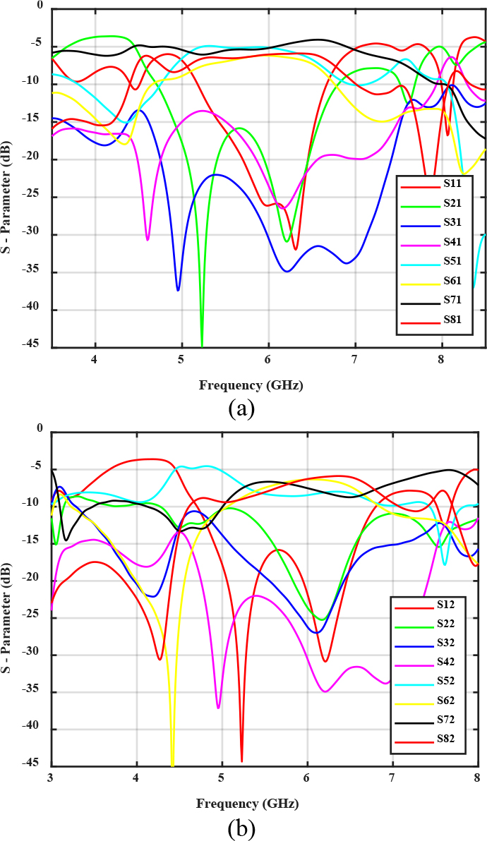
Figure 9: S-parameters of the 4 4 Butler matrix showing the S-parameter responses when (a) port 1 is excited and when (b) port 2 is excited.
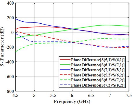
Figure 10: Output phase difference of the proposed 4 4 Butler matrix when ports 1 and 2 are excited.
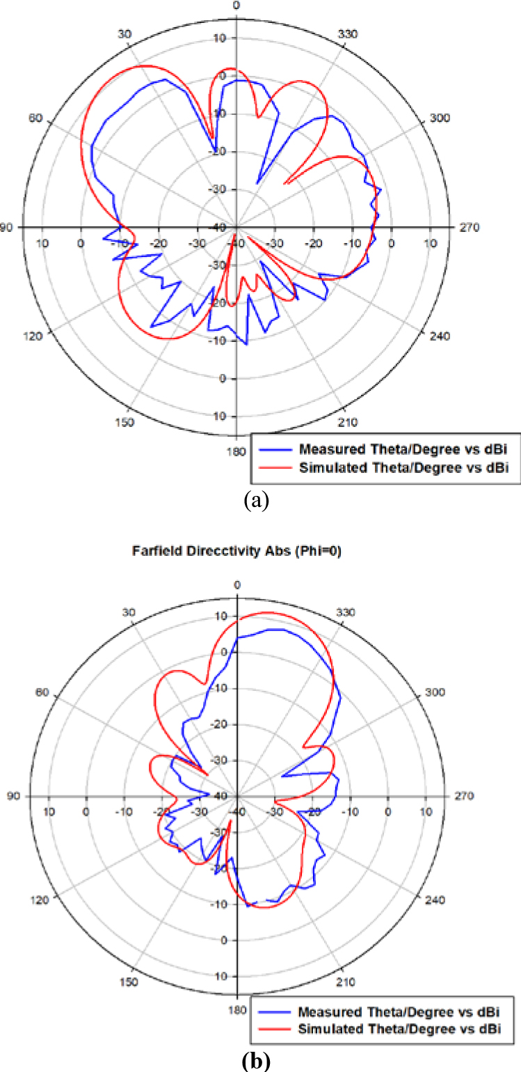
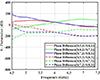
Figure 11: The measured and simulated scanned beam angles of the proposed 4 4 BM: (a) when port 1 is excited; (b) when port 2 is excited.
Also, when ports 3 and 4 are excited, the transmission coefficients at the various output ports are equal but in a reverse manner to those obtained when ports 2 and 1 are excited, respectively. It is worth noting that, when all the input ports are separately excited, return losses are similar in all the cases. From the results obtained, as shown in Figure 10, the progressive output phase differences, when excited separately from different input ports, are and with phase mismatch within at the center frequency.
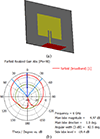
The radiation patterns of the BM beamforming network from both the simulation and the measured are shown in Figure 11. From this plot, it can be observed that when a signal is applied at the inputs port 1 or 3 and 2 or 4 separately, the scanned beam angles corresponding to each phase difference are and , respectively.
Table 4: Comparison of the proposed BM with related BM
| [2] | PCB | ||||
| [5] | SIW | ||||
| [20] | PCB | ||||
| [21] | TF-IPD | ||||
| This work | Inkjet printed |
V. CONCLUSION
In this work, a novel 4 4 BM has been designed, simulated, and fabricated using PET substrates. In terms of design, only couplers and crossover have been used without the phase shifter, typically used in case of conventional BMs. The results obtained show that the performance of the proposed design is highly reliable in terms of the radiation pattern it produced, the progressive phase difference, and amplitude imbalance at the output ports, as they are closely aligned with the theoretical predictions. From the radiation pattern measurement of the BM beamforming network, it can be observed that the beams are deposed appropriately at an angle suggested in theory. This result shows that by eliminating the phase shifter which is one of the building blocks in the design of BM, losses along the consequently shorter TL path line are minimized. Another merit of this design is the implementation of the device with a low-cost inkjet printing technique based on the chemical sintering process. With these potentials, the proposed BM can serve as a viable candidate where conformal antenna is needed and for the future 5G beamformingnetwork.
ACKNOWLEDGEMENT
The authors acknowledge the Bayero University Kano Nigeria, Universiti Teknologi Malaysia, and Multimedia University for providing financial support under Grants 5F237, 4J414, and FRGS/1/2018/TK08/MMU/02/1.
REFERENCES
[1] R. J. Gong, Y. L. Ban, J. W. Lian, Y. Liu, and Z. Nie, “Circularly polarized multibeam antenna array of ME dipole fed by 5 6 Butler matrix,” IEEE Antennas Wirel. Propag. Lett., 2019.
[2] T. Mbarek, G. Ridha, and G. Ali, “Radiation pattern of a networks antenna supplied with Butler matrix, comparison with a multi-layer structure,” Applied Computational Electromagnetics Society (ACES) Journal, pp. 1785-1792, 2007.
[3] A. K. Vallappil, M. K. A. Rahim, B. A. Khawaja, and M. Aminu-Baba, “Metamaterial based compact branch-line coupler with enhanced bandwidth for use in 5G applications,” Applied Computational Electromagnetics Society (ACES) Journal, vol. 35, no. 6, pp. 700-708, 2020.
[4] Y. S. Lin and J. H. Lee, “Miniature Butler matrix design using glass-based thin-film integrated passive device technology for 2.5-GHz applications,” IEEE Trans. Microw. Theory Tech., 2013.
[5] T. Macnamara, “Simplified design procedures for Butler matrices incorporating 90 degree hybrids or 180 degree hybrids.,” IEE Proc. H Microwaves, Antennas Propag., vol. 134, no. 1, pp. 50-54, 1987.
[6] A. Karimbu Vallappil, M. K. A. Rahim, B. A. Khawaja, and M. N. Iqbal, “Compact metamaterial based 4 4 Butler matrix with improved bandwidth for 5G applications,” IEEE Access,2020.
[7] T. Y. Chen and P. L. Chi, “Bandwidth-enhanced branch-line coupler using the center-loaded vertical line and distributed capacitors,” Asia-Pacific Microw. Conf. Proceedings, APMC, vol. 1, no. 1, pp. 989-991, 2012.
[8] C. J. Chen and T. H. Chu, “Design of a 60-GHz substrate integrated waveguide Butler matrix-a systematic approach,” IEEE Trans. Microw. Theory Tech., 2010.
[9] Q. L. Yang, Y. L. Ban, K. Kang, C. Y. D. Sim, and G. Wu, “SIW multibeam array for 5G mobile devices,” IEEE Access, 2016.
[10] W. Arriola, M. Lee, Y. Kim, E. Ryu, and I. S. Kim, “New inkjet printed wideband 3 dB branch line coupler,” IEEE MTT-S Int. Microw. Symp. Dig., pp. 1-4, 2011.
[11] K. Tekkouk, J. Hirokawa, R. Sauleau, M. Ettorre, M. Sano, and M. Ando, “Dual-Layer ridged waveguide slot array fed by a Butler matrix with sidelobe control in the 60-GHz band,” IEEE Trans. Antennas Propag., 2015.
[12] K. Wincza and S. Gruszczynski, “Broadband integrated 8 8 Butler matrix utilizing quadrature couplers and schiffman phase shifters for multibeam antennas with broadside beam,” IEEE Trans. Microw. Theory Tech., 2016.
[13] H. X. Xu, G. M. Wang, and X. Wang, “Compact Butler matrix using composite right/left handed transmission line,” Electron. Lett., 2011.
[14] Y. S. Jeong and T. W. Kim, “Design and analysis of swapped port coupler and its application in a miniaturized Butler matrix,” IEEE Trans. Microw. Theory Tech., 2010.
[15] Y. M. Madany, H. M. Elkamchouchi, and A. A. Salama, “Design and analysis of miniaturized smart antenna system using 18 switched Butler Matrix,” 2012 IEEE 13th Annu. Wirel. Microw. Technol. Conf. WAMICON 2012, vol. 2012-Janua, 2012.
[16] L. Abdelghani, T. A. Denidni, and M. Nedil, “Design of a new ultra-wideband 44 Butler matrix for beamforming antenna applications,” IEEE Antennas Propag. Soc. AP-S Int. Symp., pp. 2-3, 2012.
[17] M. Nedil, M. A. El Cafsi, T. A. Denidni, and A. Gharsallah, “Novel UWB CB-CPW Butler matrix for wireless applications,” in IEEE Antennas and Propagation Society, AP-S International Symposium (Digest), pp. 1800-1801, 2014.
[18] S. A. Babale, S. K. A. Rahim, M. Jusoh, and L. Zahid, “Branch-line coupler using PDMS and shieldit super fabric conductor,” Appl. Phys. A Mater. Sci. Process., vol. 123, no. 2, 2017.
[19] K. Wincza and S. Gruszczynski, “Broadband integrated 8 8 Butler matrix utilizing quadrature couplers and schiffman phase shifters for multibeam antennas with broadside beam,” IEEE Trans. Microw. Theory Tech., vol. 64, no. 8, pp. 2596-2604, 2016.
[20] M. Fakharzadeh, P. Mousavi, S. Safavi-Naeini, and S. H. Jamali, “The effects of imbalanced phase shifters loss on phased array gain,” IEEE Antennas Wirel. Propag. Lett., vol. 7, pp. 192-196,2008.
[21] S. Y. Zheng, W. S. Chan, and K. F. Man, “Broadband phase shifter using loaded transmission line,” IEEE Microw. Wirel. Components Lett., 2010.
[22] S. Sun and L. Zhu, “Miniaturised patch hybrid couplers using asymmetrically loaded cross slots,” IET Microwaves, Antennas Propag., 2010.
[23] G. Tian, J. P. Yang, and W. Wu, “A novel compact Butler matrix without phase shifter,” IEEE Microw. Wirel. Components Lett., 2014.
[24] H. Ren, B. Arigong, M. Zhou, J. Ding, and H. Zhang, “A novel design of 4 4 Butler matrix with relatively flexible phase differences,” IEEE Antennas Wirel. Propag. Lett., 2016.
[25] Y. S. Wong, S. Y. Zheng, and W. S. Chan, “Quasi-arbitrary phase-difference hybrid coupler,” IEEE Trans. Microw. Theory Tech., 2012.
[26] M. J. Park, “Comments on quasi-arbitrary phase-difference hybrid coupler,” IEEE Trans. Microw. Theory Tech., vol. 61, no. 3, pp. 1397-1398, 2013.
[27] S. Ahmed, F. A. Tahir, A. Shamim, and H. M. Cheema, “A compact kapton-based inkjet-printed multiband antenna for flexible wireless devices,” IEEE Antennas Wirel. Propag. Lett., vol. 14, no. c, pp. 1802-1805, 2015.
[28] Y. Kawahara, S. Hodges, B. S. Cook, C. Zhang, and G. D. Abowd, “Instant inkjet circuits: Lab-based inkjet printing to support rapid prototyping of ubicomp devices,” 2013.
[29] S. A. Babale, S. K. A. Rahim, M. Himdi, S. H. Lawan, F. D. Sani, and A. D. Usman, “Implementation of inkjet-printed 3 dB coupler with equal power division and 45 output phase difference,” Microw. Opt. Technol. Lett., vol. 63, no. 4, pp. 1007-1011, 2021.
[30] S. A. Babale, S. K. Abdul Rahim, O. A. Barro, M. Himdi, and M. Khalily, “Single layered Butler matrix without phase-shifters and crossovers,” IEEE Access, vol. 6, pp. 77289-77298,2018.
[31] C. Balanis, “Antenna theory: analysis and design, fourth edition,” in John Wiley & Sons, Inc.,2016.
BIOGRAPHIES

Suleiman Aliyu Babale (Member, IEEE) received the bachelor’s degree in electrical engineering from Bayero University Kano, Nigeria, in 2005, the M.Sc. degree from Ahmadu Bello University Zaria, Nigeria, in 2012, and the Ph.D. degree in electrical engineering with majors in telecommunications from Universiti Teknologi Malaysia, Johor Bahru, Malaysia, in 2018.
He has published more than 25 journal papers and conference and technical proceedings on antenna arrays, smart antenna systems, and microwave devices. He has been a Lecturer with Bayero University Kano since 2009 and a registered member of the Council for the Regulation of Engineering in Nigeria (COREN) since 2011. His main research interests are in millimeter-wave multi-beam antenna array with Butler matrix beamforming network for 5G wireless communications.

Sharul Kamal Abdul Rahim received the first degree from University of Tennessee, USA majoring in electrical engineering, graduating in 1996, the M.Sc. degree in engineering (communication engineering) from Universiti Teknologi Malaysia (UTM) in 2001, and the Ph.D. degree in wireless communication system from the University of Birmingham, U.K., in 2007.
Currently, he is a Professor with Wireless Communication Centre, Faculty of Electrical Engineering, UTM Skudai. His research interest is in smart antenna on communication system. He has published more than 50 journal papers and technical proceedings on rain attenuations, smart antenna system, microwave design, and reconfigurable antenna in national and international journals and conferences.
Dr. Rahim is also a member of IEEE Malaysia Section, Member Board of Engineer Malaysia (MBEM), and Member of Institute of Engineer Malaysia (MIEM) and Eta Kappa Nu Chapter (International Electrical Engineering Honor Society, University of Tennessee).

Tan Kim Geok received the B.E., M.E., and Ph.D. degrees from Universiti Teknologi Malaysia, in 1995, 1997, and 2000, respectively, all in electrical engineering.
He was a Senior R&D Engineer with EPCOS Singapore, in 2000. From 2001 to 2003, he was with DoCoMo Euro-Labs, Munich, Germany. He is currently an Academic Staff with Multimedia University. His research interests include radio propagation for outdoor and indoor, RFID, multi-user detection technique for multi-carrier technologies, and A-GPS.

Kashif Nisar Paracha received the bachelor’s degree (Hons.) in electrical engineering from the University of Engineering and Technology (UET), Taxila, Pakistan, in 2004, the M.S. degree in electrical engineering from the King Fahd University of Petroleum and Mineral (KFUPM), Dhahran, Saudi Arabia, in 2008, and the Ph.D. degree in electrical engineering from the Universiti Teknologi Malaysia (UTM), Johor Bahru, Malaysia, in 2019.
He was a Research Assistant with the Electrical Engineering Department, KFUPM, from 2006 to 2008, and he taught with the Electrical Engineering Department, The University of Faisalabad (TUF), Pakistan, from 2008 to 2011. He is currently an Assistant Professor with the Electrical Engineering Department, Government College University Faisalabad (GCUF). He has authored or coauthored over eight research journal articles and three conference articles. His research interests include communication, wearable antenna design, metamaterials, inkjet printing methods, and algorithms.
Dr. Paracha is a Life-Time Professional Member of the Pakistan Engineering Council (PEC) and Senior member of IEEE, USA.

Arslan Dawood Butt received the B.Sc. degree in electrical engineering with distinction from EME College, NUST, Pakistan, in 2010. He immediately enrolled for M.Sc. in electronic systems engineering at Politecnico di Milano, Italy and received the master’s degree in 2012.
He later pursued the Ph.D. degree in the field of “silicon based radiation detection systems” with the same university and was awarded the Ph.D. degree with Merit in 2016. During his M.S. and Ph.D. studies, Dr. Butt worked on international projects sponsored by European Space Agency, the European Commission, and the Instituto Nazionale di Fisica Nucleare (INFN) Milan section. In 2017, Dr. Butt joined the Department of Electrical Engineering, Government College University Faisalabad (GCUF), Pakistan as an Assistant Professor to pursue a career of teaching and research in Pakistan. In GCUF, Dr. Butt has changed his field of research to motion tracking and wearable sensors for augmented reality applications. He is the author and coauthor of about 16 research journal articles, and 40 conference articles.

Irfan Ali received the B.E. degree in telecommunications from the Mehran University of Engineering and Technology (MUET), Pakistan, in 2010 and the master’s degree in telecommunications engineering from the NED University of Engineering and Technology, in 2014, and the Doctor of Philosophy (Ph.D.) degree from Wireless Communication Centre (WCC), Universiti Teknologi Malaysia (UTM).
His research interests include dielectric resonator antennas, microstrip patch antennas, MIMO antennas, and mutual coupling analysis. He has published more than 20 papers in reputed journals and conference proceedings.

Sani Halliru Lawan (Member, IEEE) received the B.Eng. and M.Eng. degrees in electrical engineering from Bayero University Kano, Kano, Nigeria, in 2006 and 2013, respectively, and the Ph.D. degree in electrical engineering (photonics) from Universiti Teknologi Malaysia, in 2019.
He has been working as a Lecturer with Bayero University Kano since 2009. His research interest includes fiber propagation, optical and wireless communication systems, passive optical networks, and electrical engineering services.
ACES JOURNAL, Vol. 37, No. 2, 199–208.
doi: 10.13052/2022.ACES.J.370208
© 2021 River Publishers