Super Ultra-Wideband Planar Antenna with Parasitic Notch and Frequency Selective Surface for Gain Enhancement
Pankaj Jha1, Anubhav Kumar1, Asok De2, and Rakesh Kumar Jain1
1Department of Electronics and Communication Engineering, Shobhit Institute of Engineering and Technology (Deemed to be University), Meerut 250110, India
2Department of Electronics and Communication Engineering, Delhi Technological University (DTU), New Delhi 110042, India
pankaj.maahi@gmail.com; asok.de@gmail.com
Submitted On: January 28, 2022; Accepted On: July 13, 2022
Abstract
A compact Super ultra-wideband (SUW) antenna is discussed in this work. A rectangular radiator is modified into a tree-shaped structure with the defected partial ground to enhance the operating bandwidth. The novel rectangular parasitic with the circular slot is used as a notch in the ground plane which prevents the WLAN frequency. The proposed SUW antenna is achieving the 10 dB impedance bandwidth (IBW) from 3.5 GHz to 66.5 GHz frequency with a notched band varying from 5.0 GHz to 5.4 GHz. The bandwidth ratio (BDR) of the proposed SUW antenna is 1773.4 whereas the obtained bandwidth percentage (BW %) is 180. A modified SRR frequency selective surface (FSS) is designed for UWB application to improve the gain of the antenna. The compact unit cell of FSS is having electrical dimensions of 0.16 0.16. The antenna achieves the maximum realized gain 9.46 dB when FSS is loaded as a superstrate and up to 5.2 dB gain enhancement is observed in the UWB frequency.
Index Terms: SUW, BDR, FSS, gain enhancement, notch band.
1 INTRODUCTION
The present scenario of wireless communication demands a compact antenna design with improved data rate, large capacity and secure communication. The standard bandwidth of UWB communication is varying from 3.1 GHz to 10.6 GHz, it is preferred in short range applications [1]. To enhance the functionality of the communication system, the SUW antenna can be a better design option for long-range, short-range and many wireless applications. Further due to the large bandwidth (at least 10:1 bandwidth ratio [2]) of antenna it provides high channel capacity with higher data rate which can be advantageous for ISM band, GPS, GSM, and WLAN, defense, satellite communication, aeronautical navigation and radio astronomy [3]. Researchers proposed different structures and technologies for SUW antenna and they focused upon compactness, bandwidth % and BDR of the antenna. In [2], a monopole SUW antenna having 10 dB IBW from 2.59 – 31.14 GHz was designed in which a rectangular stub is accomplished for the improvement of impedance matching. In [3], three elliptical structures are used to design a tree-shaped radiator to obtained SUW characteristics from 0.65 – 35.61 GHz frequency. Sierpinski-shaped [4], the octagonal fractal antenna [5] with defects in the ground is used to design a SUW antenna with 1414.5 and 3015 BDR value respectively. In [6], an elliptical monopole SUW antenna is designed where a tapered feed is used for bandwidth improvement. In [7], CPW fed, Propeller-shaped radiator is designed to obtain the SUW characteristics from 3.15–32 GHz frequency. In [8], a transparent antenna is designed for SUW application obtaining BW % of 191. In [9], a gap is created between the ground plane and radiator to achieve SUW characteristics from 2.5–110 GHz frequency.
The gain of the antenna is an essential requirement in wireless communication and the EM signals can be transmitted as well as received effectively with a high gain antenna therefore to fulfil this many gain enhancement technologies are presented in the literature in which AMC [10–12], Metamaterial [13–15] and FSS [16–21] are the major techniques introduced by researchers. The Metamaterial techniques depends upon the characteristics of permittivity and permeability for the gain enhancement whereas the AMC and FSS control the grating lobes introduced by the antenna, reflect the radiations in a specific direction and increase the overall gain of the antenna. In [10], AMC technology is used in multi-band antenna where gain enhancement depends upon the reflection phase angle. In [11], rectangular loop fractal AMC is positioned parallel to the ground plane in a wideband antenna for gain enhancement. In [12], modified circular loop AMC loaded on the CPW antenna where it is working as a reflector. In [13], the dielectric superstrate is used the gain improvement and the radius of slots in the superstrate altered the effective permittivity. In [14], a metamaterial unit cell in the ground plane placed diagonally enhances the gain of a dual-band antenna. In [15], two hexagonal metamaterial cells are placed behind the antenna having double Negative metamaterial (DNG) property increases the antenna gain. In [16], a single layer FSS with the modification in loop structure is designed for the antenna operating in sub-6 GHz frequency. In [17], an FSS is designed using four asymmetric rectangular conducting elements with circular slots in one unit cell for the UWB antenna. In [18], a dual-layer FSS is designed for ISM band gain enhancement. In [19], two-layer FSS is developed accomplished with an air gap between the arrays for umbrella-shaped antenna where the UWB antenna achieved up to 4 dB gain enhancement with the FSS arrangement. In [20], FSS is accomplished with four interconnected square loop metallic paths demonstrating the stopband characteristics in the entire operating band. In [21], two layers of thin FSS are designed accomplished with cross-shape and circular-shape design in the top andbottom layer.
According to the literature analysis, the SUW antenna and FSS are designed in the proposed work with the following technical contributions and novelties.
(i) The proposed antenna is designed with a simple structure and compact electric length of 0.29 0.35 where is a wavelength of the lowest operating frequency. A very high value of BDR (1773.4) validates the compactness of discussedantenna.
(ii) A parasitic rectangular stub with a circular slot demonstrates stopband characteristics and a novel WLAN notch is achieved due to formation of parallel LC circuit.
(iii) A modified SRR structure is used to design the compact FSS unit cell with the electric dimension of 0.16 0.16 and the stopband characteristics associated in FSS superstrate are diminished from the antenna notch band.
(iv) FSS superstrate significantly enhances the realized gain up of antenna up to 5.22 dB in the UWB frequency range.
2 ANTENNA DESIGN AND EVOLUTION
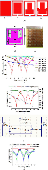
The SUW antenna and FSS is designed with FR4 substrate having dielectric constant () 4.4 and 1.6 mm substrate thickness. The proposed SUW antenna design is depicted in Figs. 1 (a) and (b), and hardware is illustrated in Fig. 1 (c). The antenna acquires a physical space of 25 (U1) 30 (U2) mm2. The SUW antenna is ensuring the dimensions details as follows, P1 = 9.5 mm, U3 = 8.5 mm, G1 = 7.1 mm, P2 = 9 mm, G2 = 11 mm, U4 = 3 mm, P3 = 5.5 mm, G3 = 11 mm, U5 = 5.5 mm, G5 = 3 mm, P4 = 5.5 mm, U6 = 5.5 mm, G6 = 2 mm, P5 = 9 mm, G4 = 4 mm, G7 = 4 mm, G8 = 3.1 mm, R = 2.75 mm and U7 = 7.5 mm.
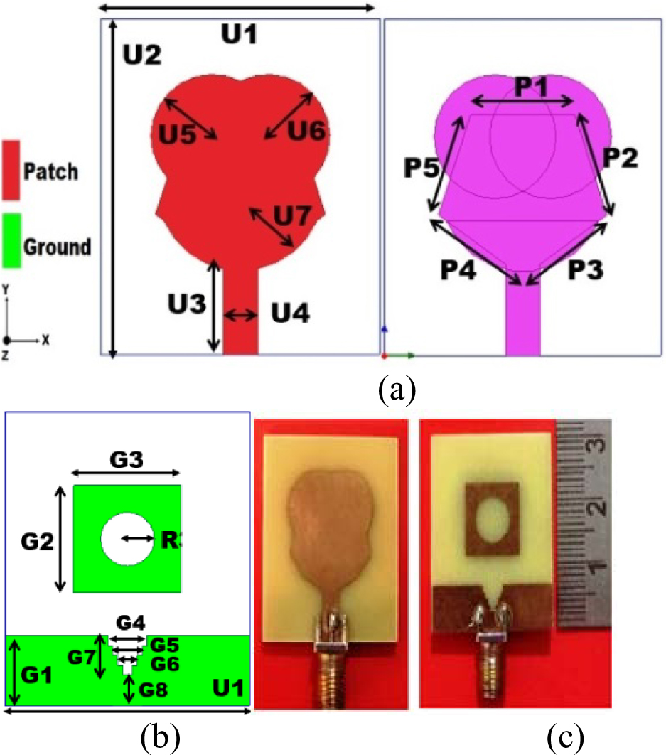
Figure 1: (a) Dimensions of top plane. (b) Dimensions of bottom plane. (c) Prototype hardware of SUW antenna.
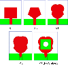
The proposed SUW antenna with parasitic stub is developed in five successive steps as depicted in Fig. 2. In step 1, a rectangular radiating patch is designed using eqn (1) [22] given below.
| (1) |
where W is the patch width of the antenna, c represents light velocity and f is the minimum operating frequency. Using above equation the obtained width of patch is 25 mm for 3.5 GHz frequency validating the antenna dimensions.
To obtain and validate 50 impedance matching of proposed work eqn (2) [22] is utilized as given below.
| (2) |
where W and h is the dimension of proposed antenna and is effective permittivity.
Further the micro-strip feed is designed with a 3 mm width and 7.5 mm length where partial groundconductor height is 7 mm. The feed is also matched with 50 11| varies from 4.3 GHz to 22.7 GHz. The radiator is modified into a polygon shape in step 2, to enhance the 10 dB IBW and improved impedance matching where |S11| varies from 3.7-23.6 GHz. Three circular stubs are consummated with the polygon-shape radiator in step 3, to convert into a tree-shape structure which increases the electric length and smoothen the current movement in the radiator and 10 dB IBW is obtained from 3.6 - 15.5 GHz and 18.1 - 24.1 GHz. Figure 3 (a) depicts the variations in |S11| of step 1 to step 3. To advance the impedance matching the stair-shaped defects are created in the bottom plane in step 4 to obtain the characteristics of SUW and 10 dB IBW is obtained from 3.5 - 66.5 GHz. In step 5, a parasitic stub with a circular slot is embedded in the ground that acts as a stopband and creates a notch from 5.0 GHz to 5.4 GHz. Figure 3 (b) depicts the variations in |S11| of step 4 & 5 and Fig. 3 (c) shows the final 10 dB IBW of SUW antenna. The presence of a circular defect in the parasitic stubs creates perturbation of current distribution and the electric current flowing on the ground has to face a longer path. This perturbation of the path creates a change in inductance (L). Similarly, the second effect of aperture in the ground plane is due to the gap located below the strip conductor. The thin gap determines an accumulation of charge and consequently can be investigated as series capacitance (C). The combination of these two singularities creates an equivalent parallel LC circuit which results in a notch band from 5.0 GHz to 5.4 GHz frequency which can prevent the WLAN frequencies in UWB applications. Figure 3 (d) is demonstrating the current circulation in the antenna with the parasitic stub.
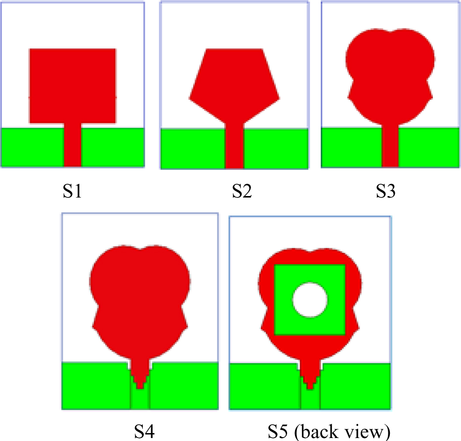
Figure 2: Development steps of SUW antenna.
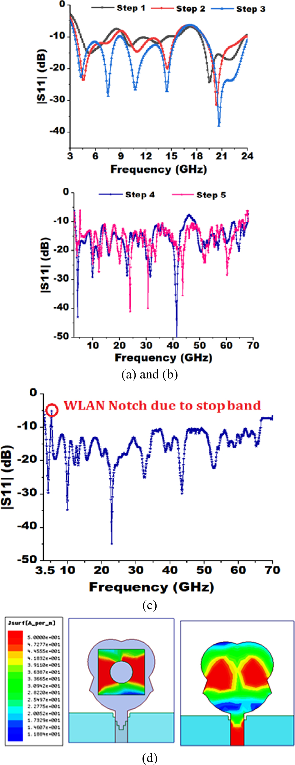
Figure 3: (a) and (b) Variation in |S11| for Step 1 to Step 5. (c) Obtained |S11| of proposed SUW antenna with notch. (d) Surface current distribution in the presence of parasitic stub and a circular slot at 5.1 GHz frequency.
3 SUW ANTENNA PARAMETERS
SUW antenna should have a BDR of 10:1, and with this BDR antenna can be designed without the restriction of predefined bandwidth. SUW antenna is used in long and short-range of communication, the parameters like BW % and BDR determines the performance of the antenna with realized gain, radiation efficiency and far-field analysis. BDR reflects the compactness as well as measures fractional usable bandwidth in SUW antenna. A higher value of BDR assures the wideband characteristics and the compactness of the antenna. It can be calculated with given eqn (3) [1].
| (3) |
where represents the electrical length and represents the electrical width of the antenna and BW% can be estimated with the given eqn (4) [1].
| (4) |
where f and f are the lower and higher frequency in operating bandwidth and center frequency f is calculated by arithmetical mean. The calculated value of BW% and BDR are 180 and 1773.4 respectively.
Table 1: Comparative study of proposed SUW antenna with the recent works
| Ref. | Size () | 10 dB IBW (GHz) | BW % | BDR |
| 2 | 0.345 0.345 | 2.59-31.14 | 169 | 1419.86 |
| 3 | 0.325 0.368 | 0.65-35.61 | 193 | 1613.7 |
| 4 | 0.347 0.358 | 1.68-26 | 175.72 | 1414.5 |
| 5 | 0.32 0.34 | 3.8-68 | 179 | 3015 |
| 6 | 0.37 0.42 | 1.02-24.1 | 183 | 1167 |
| 7 | 0.55 0.38 | 3.0-35.0 | 168 | 805 |
| 8 | 0.31 0.46 | 3.15-32 | 164 | 1102.9 |
| 9 | 0.33 0.416 | 2.5-110 | 191 | 1391 |
| Proposed work | 0.29 0.35 | 3.5-66.5 | 180 | 1773.4 |
4 FSS EVOLUTION AND ANALYSIS
The proposed FSS is designed for UWB frequency application where the FSS superstrate is positioned below the antenna. The gain enhancement in the antenna is obtained maximum when the reflection of EM waves from the FSS superstrate and radiation of the antenna is in the same direction. The FSS unit cell is designed for frequency 3.5 to 10 GHz with a modified SRR structure. The FSS evolution and FSS analysis as discussedbelow.
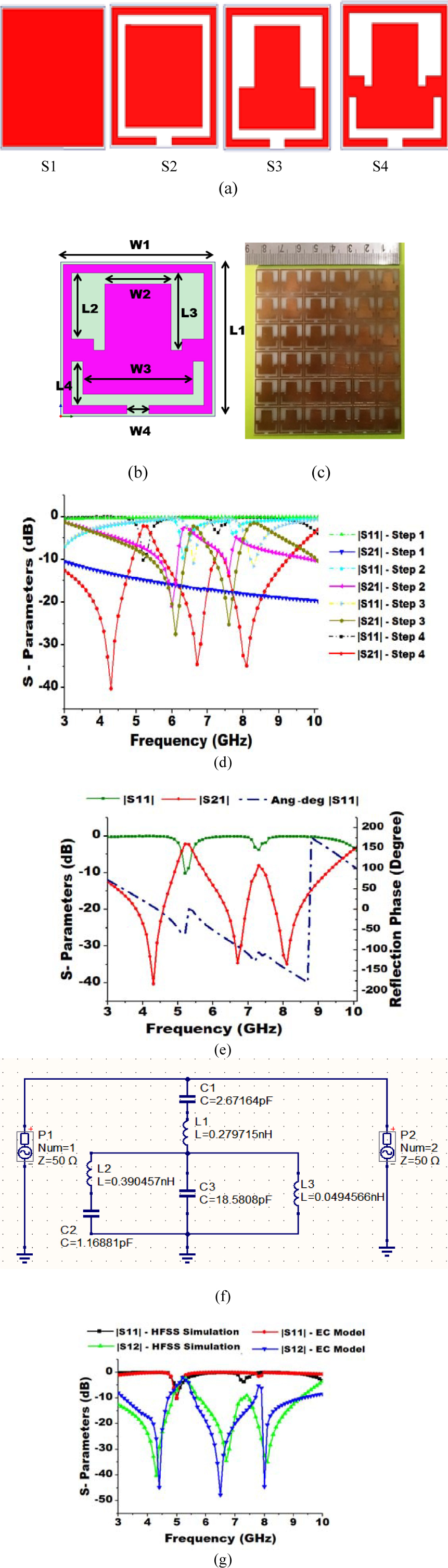
Figure 4: (a) FSS evolution steps. (b) FSS unit cell dimensions. (c) Hardware prototype of FSS. (d) S-parameters associated with evolution steps. (e) Extracted EC model of unit cell. (f) FSS s-parameters with variation in reflection phase angle. (g) S-parameters of the proposed unit cell using HFSS simulation and EC model.
4.1 FSS evolution
To determine the dimensions of the FSS superstrate eqn (5) [16] is used as given below.
| (5) |
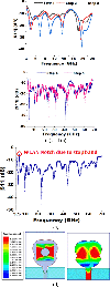
where Pr is the periodicity of the unit cell, wavelength is obtained from the maximum frequency in the operating band and incident wave angle is . At = 0 and for frequency 10 GHz, the obtained is 30 mm, therefore the dimensions of the unit cell is considered only 14 mm x 14 mm with the electric length of 0.16 0.16. The FSS unit cell is developed in four stages as depicted in Fig. 4 (a). The FSS unit cell dimensions are as follows, W2 = 4 mm, L4 = 6 mm, W1 = 14 mm, L3 = 7 mm, W4 = 2 mm, L2 = 6 mm, W3 = 10 mm and L1 = 14 mm as illustrated in Fig. 4 (b). The fabricated FSS and the s-parameters of evolution steps of the FSS superstrate are shown in Figs. 4 (c) and (d). A square shape FSS is designed in step(S)-1, to obtain stopband characteristics in UBW frequency. The |S| is varying from 3 GHz to 10 GHz, demonstrating weak stopband characteristics. In step 2, SRR is introduced with 1 mm uniform width (Fw) in the FSS unit cell to improve the stopband characteristics where |S12| is varying from 5.6 GHz to 7.2 GHz. In step 3, the structure of SRR is modified and improved |S12| bands are obtained which are varying from 5.6 GHz 7.8 GHz but still, the stopband characteristics are not obtained in the lower operating band. Finally in step-4, the FSS unit cell is further modified which increase the electric length and improves the stopband characteristics but keeping in the mind the notch characteristics of the antenna, the stopband characteristics mitigate from the unit cell. The final |S12| is varying from 3.0 GHz to 10 GHz except notch band where it reveals that stopband characteristics are diminished from the results where the antenna demonstrates the notch band. The phase angle of |S11| varies linearly in entier frequency range and decreases when the frequency is increasing except the notch band as shown in Fig. 4 (e).
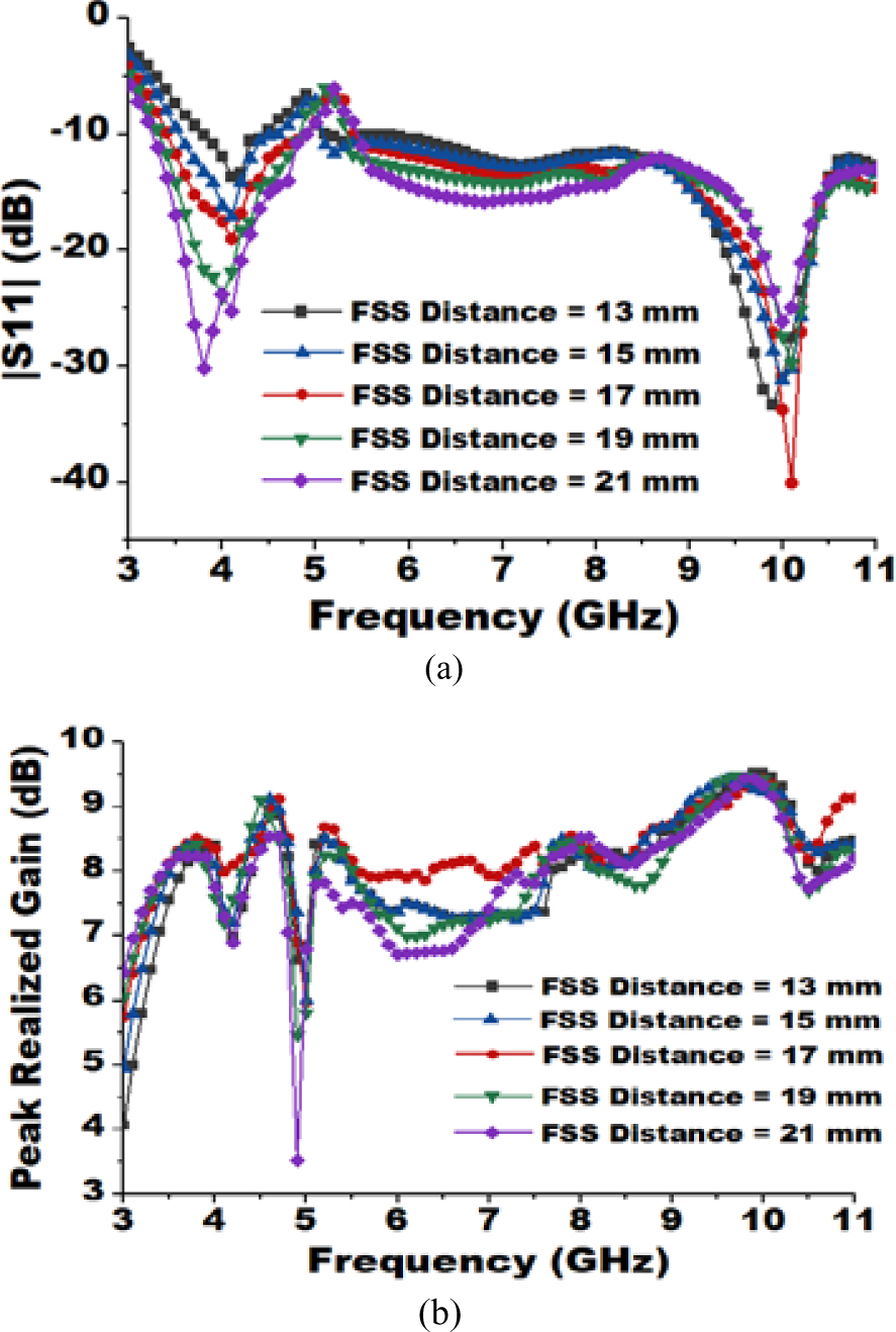
Figure 5: (a) |S11|. (b) Realized gain at different distance between FSS and proposed antenna.
The equivalent circuit (EC) model of the FSS unit cell is designed using QUCS software with lumped components as depicted in Fig. 4 (f). The lumped elements of the circuit are determined from the eqn (6) and (7) [16] where three capacitive elements C1, C2 and C3 have values of 2.67 pF, 1.16 pF and 18.58 pF along with three inductive elements L1, L2 and L3 with values of 0.276 nH, 0.39 nH and 0.049 nH.
| (6) |
| (7) |
where w1, L1, the FSS width, length, h is the and is the incidence angle. The extracted s-parameters from EC model are compared with the simulated values using HFSS-13 simulator as depicted in Fig. 3 (g) where both are having similar variations. The advance simulation techniques as a prospective are used to extract the solution for nonconformal meshes of EM wave [24], To solve anisotropic Maxwell’s equations [25] and Phase Synthesis of Beam-Scanning in Deep Learning Technique [26].
Table 2: Comparative analysis of proposed gain enhancement technology with the other recent works
| Ref. | Antenna Size (mm2) | Technology used | Operating Band (GHz) | Gain Enhancement (dB) |
| 11 | 64 64 | AMC | 3.36, 5.96, 9.09 | 3.58 |
| 12 | 70 70 | AMC | 1.9–6.95 | 3.06 |
| 14 | 38 38 | Metamaterial | 2.4–5.82 | 3.69 |
| 16 | 35 25 | Metamaterial | 5.6–10.3 | 3.2 |
| 17 | 30 30 | Single layer FSS | 3.6–6.1 | 4.0 |
| 18 | 20 27 | Single layer FSS | 4.7–14.9 | 4.5 |
| 19 | 63.65 51.16 | Single/dual layer FSS | 2.4 | 4.4 |
| 20 | 35 30 | Single layer FSS | 3.0–13.4 | 4 |
| 21 | 40 30 | Dual-layer FSS | 8.1–13.2 | 3.3 |
| Proposed work | 25 30 | Single layer FSS | 3.5–11.0 | 5.2 |
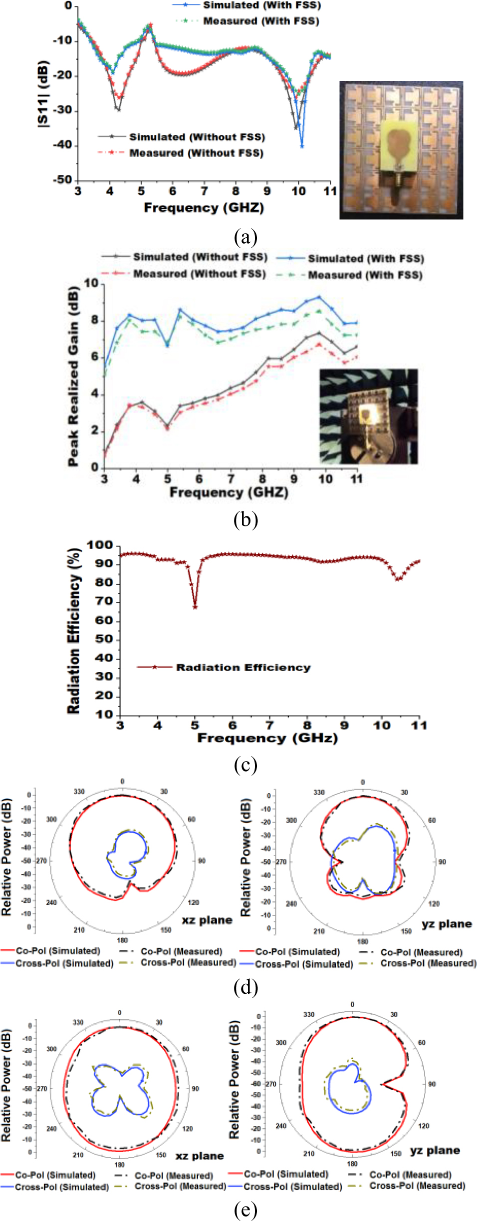
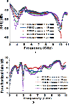
Figure 6: (a) Measured |S11| with simulated values. (b) Measured peak gain. (c) Radiation efficiency. (d) and (e) Radiation patterns at frequency 4.1 GHz and 7.50 GHz in x-z and y-z coordinates with FSS superstrate.
4.2 FSS analysis
The separation of FSS superstrate from the antenna is the vital parameter for gain enhancement and it can be calculated with eqn (8) [16] as given below.
| (8) |
In the equation, F is the distance of the antenna from FSS and K is constant which is equal to 2. The value of N can be chosen for any integer value and is the wavelength at which the reflection phase is zero. The reflection phase is 0 at 4.4 GHz frequency as depicted in Fig. 4 (e) and at this frequency, the value of /4 is 17.02 mm. Keeping this in mind that the position of FSS is varied from 13 mm to 21mm and the variation in |S11| and peak gain are observed. The |S11| of antenna is having minor variations after the notch band irrespective of the FSS superstrate position but the lower operating bandwidth reduces when FSS distance behind the antenna decreases as depicted in Fig. 5 (a). The peak gain with the FSS superstrate at different placement is illustrated in Fig. 5 (b) where at the 17 mm distance, the minimum variations are observed and maximum gain enhancement is achieved 5.2 dB. Therefore 17 mm optimum distance is finalized between FSS superstrate and antenna where the 10 dB IBW is varying from 3.5 GHz to 11 GHz and the peak gain is having a maximum value of 9.46 dB.
5 RESULT AND DISCUSSION
HFSS-13 software is used to simulate the proposed antenna and FSS design whereas experimental results of |S11| are obtained by Anritsu-MS2038C VNA and the far-field analysis is done in the anechoic chamber. The simulated |S11| of the antenna is varying from 3.5 GHz to 66.5 GHz with a WLAN notch band from 5 GHz to 5.4 GHz. As per VNA availability the |S11| measurement is carried out up to 11 GHz with and without FSS and the measured results have similarities with the simulated values as shown in Fig. 6 (a). The measured gain of the discussed antenna is shown in Fig. 6 (b) where the measured gain is having minor deviations which are less than 0.5 dB in the presence of FSS also. The gain enhancement is achieved up to 5.2 dB using a single layer FSS. The simulation radiation efficiency is found more than 85 % except for the notch band as illustrated in Fig. 6 (c). The measured and simulated radiation pattern with FSS are illustrated in Figures 5 (e) and 6 (d), at two centre frequencies in the x-z and y-z coordinate system which are demonstrating the omnidirectional radiation pattern. The comparative analysis with related work of SUW antenna is given in Table 1, which authorizes that the presented tree-shaped antenna is compact having an electrical length of 0.29 0.35 The BW % of the SUW antenna is 180 with a high value of BDR which is 1773.4. The gain enhancement with a single layer and single-sided FSS superstrate is compared with gain improvement existing technology in Table 2; it reveals that the proposed FSS enhances the gain effectively in the entire operating band up to 5.2 dB.
6 CONCLUSION
The tree-shaped SUW antenna is designed with a novel parasitic stub in the ground demonstrating notch characteristics. The tree-shaped radiator is improving the operating bandwidth whereas defected ground enhances the impedance matching in the antenna. The parasitic stub with a circular slot in the bottom plane creates a WLAN notch in the antenna. The high value of BDR confirms the compactness of the proposed SUW antenna. The modified SRR based single-layer FSS superstrate is placed below the antenna which reflects the grating lobes and enhances the antenna gain up to 5.2 dB.
REFERENCES
[1] W. Balani, M. Sarvagya, T. Ali, M. M., Manohara Pai, J. Anguera, A. Andujar, and S. Das, “Design techniques of super-wideband antenna–existing and future prospective,” IEEE Access, vol. 7,2019.
[2] T. Okan, “A compact octagonal ring monopole antenna for super wideband applications,” Microw. Opt. Technol. Lett., vol. 62, no. 3, pp. 1237-1244, 2020.
[3] S. Singhal and A. K. Singh, “Elliptical monopole based super wideband fractal antenna,” Microw. Opt. Technol. Lett., vol. 62, no. 3, pp. 1324-1328, 2020.
[4] C. Á. Figueroa Torres, J. L. Medina Monroy, H. Lobato Morales, R. A. Chávez Pérez, and A. Calvillo Téllez, “A novel fractal antenna based on the Sierpinski structure for super wide band applications,” Microw. Opt. Technol. Lett., vol. 59, no. 5, pp. 1148-1153, 2017.
[5] S. Singhal and A. K. Singh, “CPW-fed hexagonal Sierpinski super wideband fractal antenna,” IET Microw. Antennas Propag., vol. 10, no. 15, pp. 1701-1707, 2016.
[6] J. Liu, S. Zhong, and K. P. Esselle, “A printed elliptical monopole antenna with modified feeding structure for bandwidth enhancement,” IEEE Trans. Antennas Propag., vol. 59, no. 2, pp. 667-670, 2010.
[7] A. Gorai, A. Karmakar, M. Pal, and R. Ghatak, “A CPW-fed propeller shaped monopole antenna with super wideband characteristics,” Progress Electromagn. Res. C, vol. 45, pp. 125-135,2013.
[8] S. Hakimi, S. K. A. Rahim, M. Abedian, S. M. Noghabaei, and M. Khalily, “CPW-fed transparent antenna for extended ultrawideband applications,” IEEE Antennas Wireless Propag. Lett., vol. 13, pp. 1251-1254, 2014.
[9] A. Seyfollahi and J. Bornemann, “Printed-circuit monopole antenna for super-wideband applications,” pp. 654-655, 2018.
[10] A. Ghosh, “Gain enhancement of triple-band patch antenna by using triple-band artificial magnetic conductor,” IET Microwaves, Antennas Propag., vol. 12, no. 8, Art. no. 1400, 2018.
[11] B. Zhang, P. Yao, and J. Duan. “Gain-enhanced antenna backed with the fractal artificial magnetic conductor,” IET Microw. Antennas Propag., vol. 12, no. 9, Art. no. 1457, 2018.
[12] K. N. Paracha, “A dual band stub-loaded AMC design for the gain enhancement of a planar monopole antenna,” Microw. Opt. Technol. Lett., vol. 60, no. 9, 2018.
[13] J. H. Kim, C.-H. Ahn, and J.-K. Bang, “Antenna gain enhancement using a holey superstrate,” IEEE Trans. Antennas Propag., vol. 64, no. 3, Art. no. 1164, 2016.
[14] S. Roy and U. Chakraborty, “Gain enhancement of a dual-band WLAN microstrip antenna loaded with diagonal pattern metamaterials,” IET Commun., vol. 12, no. 12, Art. no. 1448, 2018.
[15] N. Rajak, N. Chattoraj, and R. Mark, “Metamaterial cell inspired high gain multiband antenna for wireless applications,” AEU-Int. J. Electron. Commun., vol. 109, pp. 23, 2019.
[16] A. Kumar, A. De, and R. K. Jain, “Gain enhancement using modified circular loop FSS loaded with slot antenna for sub-6 GHz 5G application,” Progress Electromagn. Res. Lett., vol. 98, pp. 41-48, 2021.
[17] P. Das and K. Mandal, “Modelling of ultra-wide stop-band frequency-selective surface to enhance the gain of a UWB antenna,” IET Microw. Antennas Propag., vol. 13, no. 3, pp. 269-277, 2019.
[18] M. A. Belen, “Performance enhancement of a microstrip patch antenna using dual-layer frequency-selective surface for ISM band applications,” Microw. Opt. Technol. Lett., vol. 60, no. 11, pp. 2730-2734, 2018.
[19] S. Kundu, A. Chatterjee, S. K. Jana, and S. K. Parui, “A compact umbrella-shaped UWB antenna with gain augmentation using frequency selective surface,” Radio Eng., vol. 27, no. 2, pp. 448-454,2018.
[20] G. S. Paul, K. Mandal, and A. Lalbakhsh, “Single-layer ultra-wide stop-band frequency selective surface using interconnected square rings,” AEU-Int. J. Electron. Commun., vol. 132, 2021.
[21] A. Bhattacharya, B. Dasgupta, and R. Jyoti, “Design and analysis of ultrathin X-band frequency selective surface structure for gain enhancement of hybrid antenna,” Int. J. RF Microw. Comput.-Aided Eng., 2020.
[22] A. F. Alsager, Design and Analysis of Microstrip Patch Antenna Arrays, 2011.
[23] Q. Y. F. Zhan, M. Zhuang, M. Yuan, and Q. H. Liu, “Stabilized DG-PSTD method with nonconformal meshes for electromagnetic waves,” IEEE Trans. Antennas Propag., vol. 68, no. 6, pp. 4714-4726, 2020.
[24] Q. Zhan, Y. Wang, Y. Fang, Q. Ren, S. Yang, W.-Y. Yin, and Q. H. Liu, “An adaptive high-order transient algorithm to solve large-scale anisotropic Maxwell’s equations,” IEEE Trans. Antennas Propag., vol. 70, no. 3, pp. 2082-2092, 2022.
[25] T. Shan, M. Li, S. Xu, and F. Yang, “Phase synthesis of beam-scanning reflectarray antenna based on deep learning technique,” Progress Electromagn. Res., vol. 172, pp. 41-49, 2021.
BIOGRAPHIES

Pankaj Jha received B. Tech and M. Tech degree from Uttar Pradesh Technical University (Now AKTU), Lucknow, UP, India, He is currently pursuing Ph.D from Shobhit Institute of Engineering and Technology, (Deemed to be University) Meerut, UP, India. His research area includes micro strip antenna, Metamaterial inspired antenna, MIMO, FSS and wearable antenna.

Anubhav Kumar received B. Tech and M.Tech from Uttar Pradesh Technical University (Now AKTU), Lucknow, UP, India. He is currently pursuing Ph.D from Shobhit Institute of Engineering and Technology, (Deemed to be University) Meerut, UP, India. He has published many SCIE/ESCI and Scopus indexed research papers. His research interests include microstrip antenna, metamaterial, FSS, MIMO, Wearable antenna, EBG and Image processing.

Asok De did his Ph.D from Indian Institute of Technology, Kharagpur. He served as faculty at University of Delhi, University of Kolkata from 1984 to 1997. He was the founder Principal of Ambedkar Institute of Advanced Communication Technology and Research (2005-2012). He served National Institute of Technology Patna and Durgapur as a Director from 2012 to 2017. Professor De has published more than 200 research papers in International Journals and International conferences. He supervised 16 Ph.D scholars till now.
ACES JOURNAL, Vol. 37, No. 7, 757–764.
doi: 10.13052/2022.ACES.J.370702
© 2022 River Publishers