Design and Development of Substrate Integrated Waveguide Based Filtenna for X Band Application
G. S. Annie Grace Vimala, V. R. Prakash, A. Akilandeswari, D. Sungeetha, and
M. Saravanan
1Department of Electronics and Communication Engineering, Saveetha School of Engineering, SIMATS, Chennai 602105, India
anniegracevimalags.sse@saveetha.com, akilandeswaria.sse@saveetha.com, sungeethad.sse@saveetha.com
2Department of Electronics and Communication Engineering, Hindustan Institute of Technology and Science, Chennai 603103, India
Prakashkrishna53@gmail.com
3Department of Electronics and Communication Engineering, Vel Tech Rangarajan Dr. Sagunthala R&D Institute of Science and Technology, Chennai 600062, India
msarawins@gmail.com
Submitted On: August 24, 2021; Accepted On: February 8, 2022
Abstract
In this paper, substrate integrated waveguide based filtenna operating at X band is proposed. The model is designed on a low-loss dielectric substrate having a thickness of 1.6 mm and comprises shorting vias along two edges of the substrate walls. To realize a bandpass filter, secondary shorting vias are placed close to primary shorting vias. The dimension and position of the vias are carefully analyzed for X band frequencies. The model is fabricated on Roger RT/duroid 5880 and the performance characteristics are measured. The proposed model achieves significant impedance characteristics with wider bandwidth in the X band. The model also achieves a maximum gain of 7.46 dBi in the operating band, thus making it suitable for X band applications.
Keywords: Antenna radiation patterns, filtenna, microstrip patch, rectangular wave guide (RWG), substrate integrate waveguide (SIW).
I. INTRODUCTION
Due to the increase in demand for multifunctional antennas in wireless communications, the size of the antenna profile is greatly reduced and also provides better feasibility in integration with high-frequency circuits. Recently, filtenna becomes popular since the RF space is occupied with much of the available spectrum, and, hence, the role of the filter along with the antenna becomes crucial. The substrate integrated waveguide (SIW) has proven to be a good choice because of its modular integration and low cost [1]. Most of the literature discusses the design of filter and antenna separately and are coupled with a impedance matching circuit which consumes much space in the antenna profile [2]. This can be replaced by placing a single filtenna design which reduces the overall antenna profile and also eliminates the need for an additional impedance matching circuit [3]. Utilization of both SIW technology along with filtenna further improves the antenna profile size and also improves the ease of fabrication and integration [4–6]. A compact SIW-based filtenna comprising the parasitic patch is proposed [7]. The model utilized a half-mode substrate integrated rectangular cavity to reduce its overall antenna size. In [8], an analysis of SIW structure for rat race couple is proposed. An SIW-based filtenna with reconfigurable nulls by means of electric and magnetic coupling structure is demonstrated [9]. Filtenna can also be designed by utilizing the synthesis of filter structures by placing vertical cavities as in [10]. Similarly, the filtenna can also be realized by placing three vertical cavities integrated with each other to achieve a wider FBW ratio. However, an increasing number of filter cavities to improve FBW results in wider profile thickness. A low-profile SIW-based filtenna is reported [11] with improved bandwidth characteristics that utilize a complementary split-ring resonator (CSRR) over the SIW structures. Most of the literature discusses filtenna operating at narrowband and also these filtenna are designed at lower operating frequencies with lossy transmission lines or with other complex geometries. Hence, there is need for designing filtenna with wide operating range and also with better miniaturization. In this paper, an SIW-based filtenna with improved bandwidth and radiation characteristics is proposed. The antenna is modeled on a low-loss roger substrate with a profile thickness of 1.6 mm which makes it feasible for the integration of other high-frequency circuits. The antenna is analyzed and fabricated to measure its performance characteristics and compared with other conventional models. Moreover, the filtenna exhibits sharp cutoff bands around the operating bands which makes it ideal for X band applications.
II. SUBSTRATE INTEGRATED WAVEGUIDE GEOMETRY
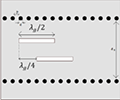
The dielectric-filled metallic waveguide can be realized by means of substrate integrated waveguide [12] which exhibits similar propagation characteristics. The design of the proposed antenna is as shown in Figure 1. The width “W” of SIW is calculated from center-to-center distance between the rows of vias. Each via has spacing “p” and has radius “r.” The length of dielectric layer is “L.” Let a and b denote the width and height of the rectangular waveguide, respectively. Assuming a b, the propagating mode with the lowest cutoff frequency is TE10 (dominant mode). We calculate the radius of via using
| (1) |

Figure 1: SIW geometry. geometry.
The cutoff frequency of each propagating mode
| (2) |
where C is the speed of light in vacuum, m and n are mode numbers, and a and b are dimensions of the waveguide. For mode, the cutoff frequency is given as . For SIW, the dimension is the distance between the SIW walls and is given by , where where d is the diameter of via and p (p must satisfy p 2d) is the distance between the vias. The guided wavelength is calculated from and d must satisfy.
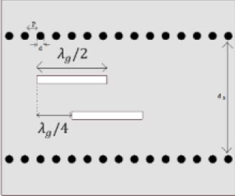
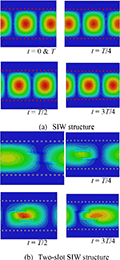
Figure 2: Two-slot SIW.
Based on the design equations, the geometry of the SIW along with two-slot geometry is shown in Figures 1 and 2 and its corresponding dimensions are given in Table 1 .
Table 1: Geometry of SIW
| 9.25 mm | |
| L B | 25 mm 30 mm |
| P | 2 mm |
| d | 1 mm |
| 15.77 mm |
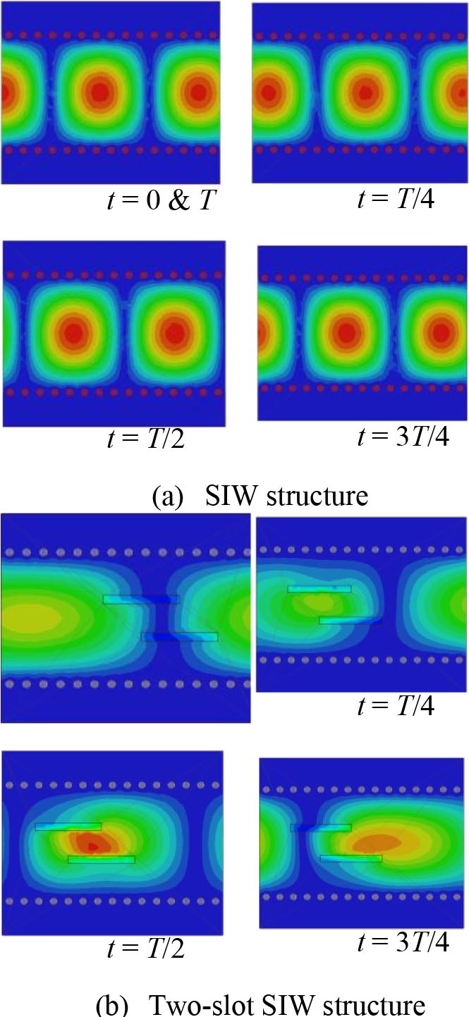
Figure 3: Two-slot SIW.
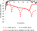
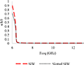
The surface current distribution at different instances of time “t” over the geometry is shown in Figure 3. The surface current distribution exhibits sinusoidal variation in the variations of the field on the surface of the structure and is confined within the SIW walls above its operating frequency. The antenna is modeled on roger duroid 5880tm having a relative permittivity of 2.2 and thickness of 1.6 mm. The 10 dB reflection coefficient curve corresponding to both SIW with and without slot geometry is given in Figure 4. The structure achieves 10 dB impedance characteristics over its entire operating X band which comprises 8–12 GHz with a cutoff frequency of 6.5 GHz.
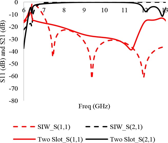
Figure 4: Reflection and transmission coefficients (dB).
SIWs have similar radiation characteristics when compared to dielectric filled metallic waveguide as shown in Figure 4 (S plot). Hence, longitudinal slots having a length of g/2 are incorporated in the SIW structure which behaves like a resonant mode in the operating band. The phase constant corresponding to the fundamental TE10 mode for given slotted SIW isgiven by
| (3) |
where is the wave number. Figure 5 shows the normalized phase constant corresponding to SIW compared with slotted SIW structure. It is observed that the structure attains real phase value whose mode propagates above the cutoff frequency of 6.5 GHz.
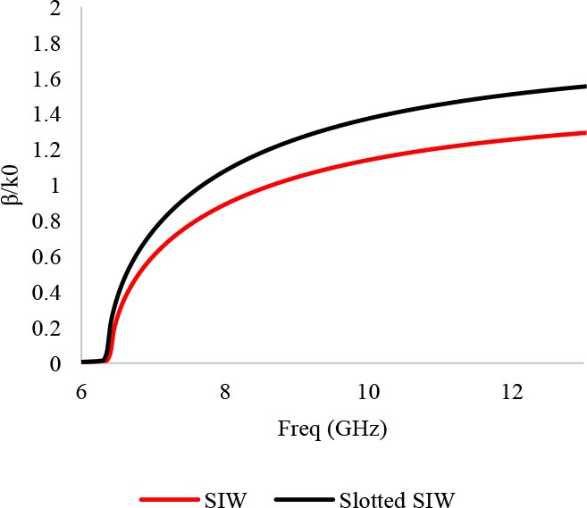
Figure 5: Normalized phase constant .
The attenuation constant is given by
| (4) |
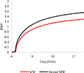
where L is the aperture length. Figure 6 shows the normalized attenuation characteristics of the SIW compared with slotted SIW structure. It is inferred that the structure attains minimum attenuation at its operating band. The dispersion characteristics of the antenna are determined from phase constant and attenuation constant of the proposed SIW structure.
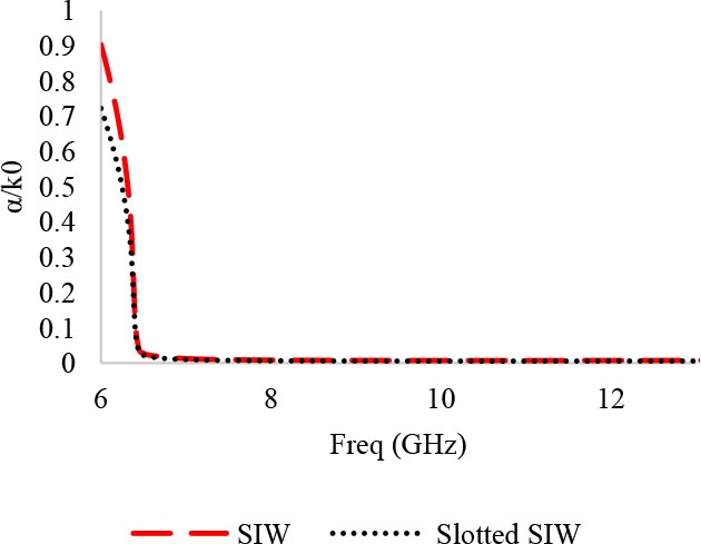
Figure 6: Normalized attenuation constant
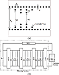
III. HIGHER ORDER INDUCTIVE BASED FILTER DESIGN
A higher order inductive filter is proposed as shown in Figure 5. The filter comprises metallic vias placed to provide inductive window having a width of and length of the cavity resonators are given by as shown in Figure 5. The coupling coefficient between the filter sections is given by K and the resonating frequency of the filter is given by
| (5) |
where .
IV. SIW-BASED FILTENNA
The proposed antenna geometry is integrating both SIW and filtenna as shown in Figure 7. The model utilizes microstrip to SIW transition [12] connected to microstrip line and integrated with SIW. The feed line is tapered need the antenna feeding point for better matching the impedance of the SIW structure with the input. The width and length of the tapered section are designed and optimized for impedance matching especially at higher frequencies.
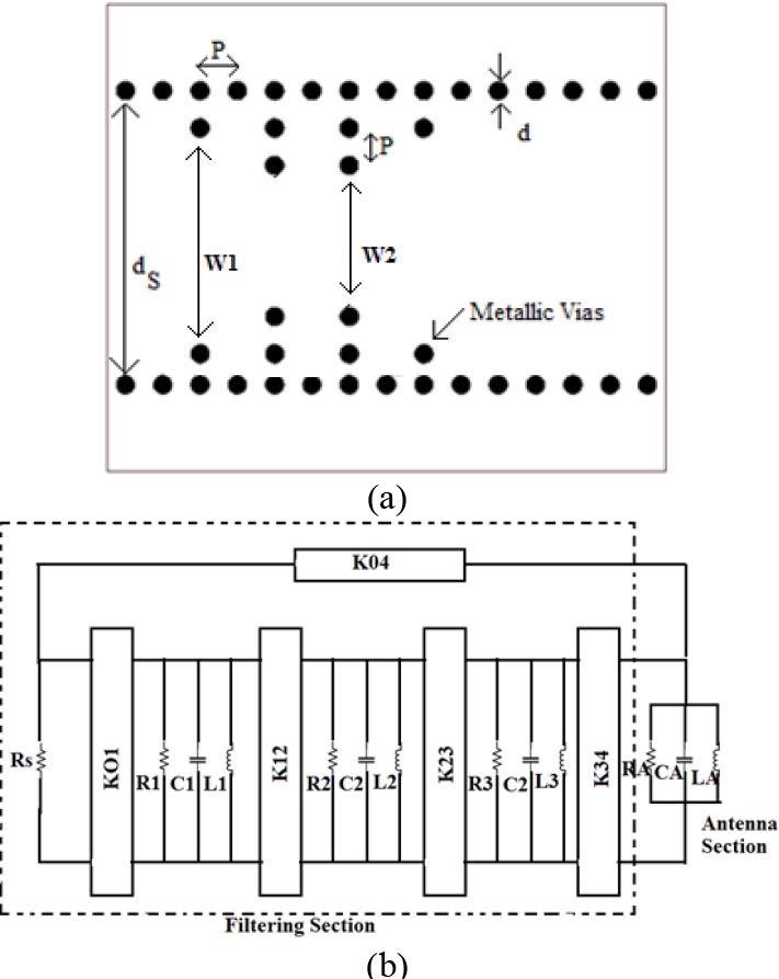
Figure 7: Higher order inductive filter.
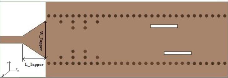
Figure 8: Proposed SIW-based filtenna.
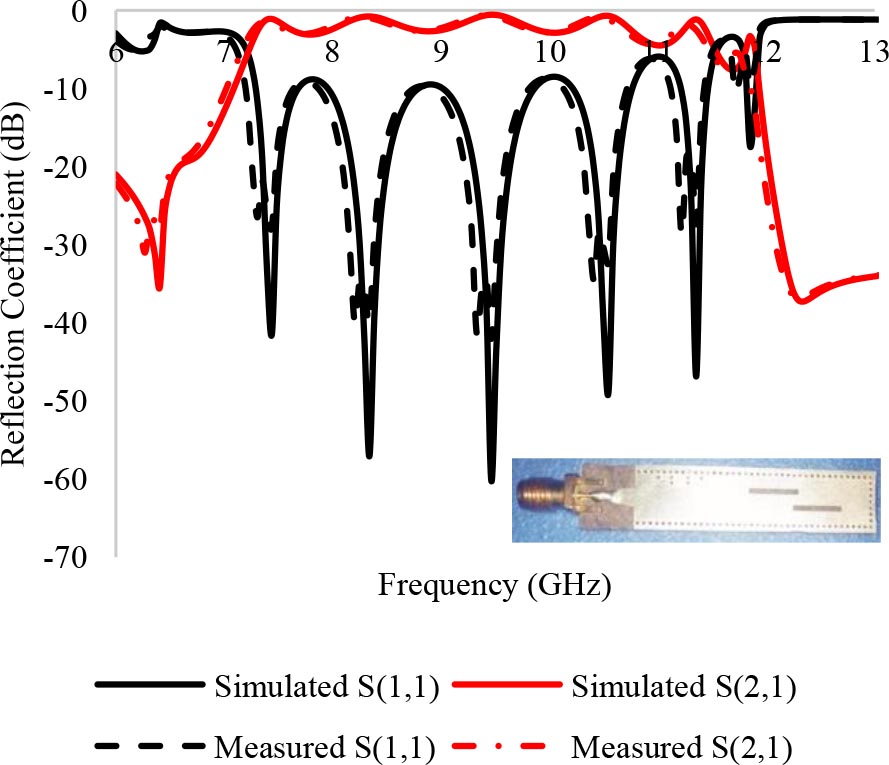
Figure 9: Impedance characteristics of filter design.
The antenna is fabricated on low-cost roger substrate having a relative permittivity of 2.2 and a thickness of 1.6 mm. The model is connected with SMA connector.
In order to validate the performance characteristics of the antenna model, the performances of the prototype are measured and are compared with simulated results.
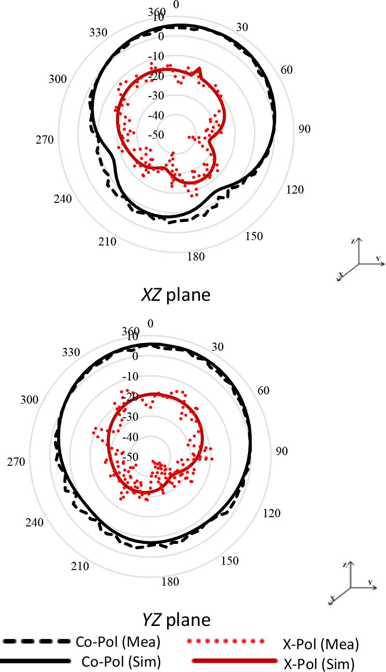
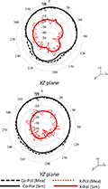
Figure 10: Radiation characteristics.
The impedance characteristics of the filtenna for both simulated and measured results are shown in Figure 8. The reflection coefficient curve corresponding to filtenna geometry achieves 10 dB impedance characteristics over its entire operating X band which comprises 8–12 GHz with sharp rolloff around its operating band. The radiation characteristics of the antenna are measured by the three-antenna gain method and the gain of the proposed model is calculated by means of the Friss transmission equation given below
| (6) |
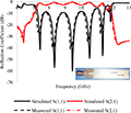
The simulated and measured radiation characteristics of the antenna model are shown in Figure 9. The antenna radiation pattern is measured inside the anechoic chamber. The antenna achieves a symmetrical radiation pattern with a peak gain of 7.18 dBi for simulated and 6.94 dBi for measured at its 10 GHz center frequency in the operating band (8–12 GHz). Since the ground plane is limited due to its size limit, there is small amount of back radiation seen in the radiation pattern.

Figure 11: Realized gain (dBi).
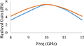
The proposed antenna is placed in line of sight with transmitting antenna inside the anechoic chamber. The realized gain corresponding to the proposed antenna is noted for different frequencies in the operating band and is compared with simulated gain as shown in Figure 10.
V. CONCLUSION
A compact SIW-based filtenna operating at X band frequencies is proposed. The model utilizes filter section integrated with SIW-based slotted section. The microstrip to taper transition is used for impedance matching and is terminated with transmission line. The model is analyzed for dispersion characteristics and is fabricated on low-cost substrate. The prototype attains resonates at 8–12GHz in the X band region with a peak gain of 7.18 dBi for simulated and 6.94 dBi for measured at its resonant frequency.
REFERENCES
[1] Y. Cassivi, L. Perregrini, P. Bressan, K. Wu, and G. Conciauro, “Dispersion characteristics of substrate integrated rectangular waveguide,” IEEE Microw. Compon. Lett., vol. 12, no. 2, pp. 333–335, Feb. 2002.
[2] K. Zhou, C.-X. Zhou, and W. Wu, “Resonance characteristics of substrate-integrated rectangular cavity and their applications to dual-band and wide-stopband bandpass filters design,” IEEE Trans. Microw. Theory Techn., vol. 65, no. 5, pp. 1511–1524, May 2017.
[3] M.-C. Tang, Y. Chen, and R. W. Ziolkowski, “Experimentally validated, planar, wideband, electrically small, monopole filtennas based on capacitively loaded loop resonators,” IEEE Trans. Antennas Propag., vol. 64, no. 8, pp. 3353–3360, Aug. 2016.
[4] K. Xu, J. Shi, X. Qing, and Z. N. Chen, “A substrate integrated cavity backed filtering slot antenna stacked with a patch for frequency selectivity enhancement,” IEEE Antennas Wireless Propag. Lett., vol. 17, no. 10, pp. 1910–1914, Oct. 2018.
[5] K.-Z. Hu, M.-C. Tang, M. Li, and R. W. Ziolkowski, “Compact, low-profile, bandwidth-enhanced substrate integrated waveguide filtenna,” IEEE Antennas Wireless Propag. Lett., vol. 17, no. 8, pp. 1552–1556, Aug. 2018.
[6] K. Dhwaj, J. M. Kovitz, H. Tian, L. J. Jiang, and T. Itoh, “Half-mode cavity based planar filtering antenna with controllable transmission zeroes,” IEEE Antennas Wireless Propag. Lett., vol. 17, no. 5, pp. 833–836, May 2018.
[7] K. Hu, M. Tang, D. Li, Y. Wang, and M. Li, “Design of Compact, Single-Layered Substrate Integrated Waveguide Filtenna With Parasitic Patch,” IEEE Transactions on Antennas and Propagation, vol. 68, no. 2, pp. 1134-1139, Feb. 2020, doi: 10.1109/TAP.2019.2938574.
[8] R. Dehdasht-Heydari, K. Forooraghi, and M. Naser-Moghadasi, “Efficient and Accurate Analysis of a Substrate Integrated Waveguide (SIW) Rat-Race Coupler Excited by Four U-Shape Slot-Coupled Transitions”, Applied Computational Electromagnetics Society (ACES) Journal, vol. 30, no. 1, pp. 42-49, Feb. 2015.
[9] C. Wang, X. Wang, H. Liu, Z. Chen, and Z. Han, “Substrate Integrated Waveguide Filtenna With Two Controllable Radiation Nulls,” IEEE Access, vol. 8, pp. 120019-120024, 2020, doi: 10.1109/ACCESS.2020.3005948.
[10] Y. Yusuf, H. T. Cheng, and X. Gong, “A seamless integration of 3-D vertical filters with highly efficient slot antennas,” IEEE Trans. Antennas Propag., vol. 59, no. 11, pp. 4016–4022, Nov. 2011.
[11] K. Hu, M. Tang, M. Li, and R. W. Ziolkowski, “Compact, Low-Profile, Bandwidth-Enhanced Substrate Integrated Waveguide Filtenna,” IEEE Antennas and Wireless Propagation Letters, vol. 17, no. 8, pp. 1552-1556, Aug. 2018, doi: 10.1109/LAWP.2018.2854898.
[12] D. Deslandes and K. Wu, “Integrated microstrip and rectangular waveguide in planar form”, IEEE Microwave Wireless Compon Lett., vol. 11, pp. 68–70, 2001.
[13] J. E. Rayas-Sanchez and V. Gutierrez-Ayala, “A general EM-based design procedure for single-layer substrate integrated waveguide interconnects with microstrip transitions,” 2008 IEEE MTT-S International Microwave Symposium Digest, pp. 983-986, 2008, doi: 10.1109/MWSYM.2008.4632999.
BIOGRAPHIES

Dr. G. S. Annie Grace Vimala is currently working as a professor in the department of signal and image processing, institute of ECE, saveetha school of engineering, simats, chennai, india. she did her ph.d in B.S. Aabdur Rahman university, Chennai, India. Her area of research interest includes medical image processing, electronics and pattern recognition. she has published more than 10 papers in indexed journals and also been a reviewer for Scopus and SCI journals.

Dr. V. R. Prakash faculty in the Department of Electronics and Communication Engineering, in HITS, Chennai, India. His major research work on Video processing and Image processing He is an active IEEE member and has published paper in Scopus and Web of science.

Dr. A. Akilandeswari completed her PhD in Electronics and Communication Engineering with specializing in Low Power VLSI. Her post-graduation was in Embedded systems technologies. She is presently working as an Associate Professor in Department of Electronics and communication Engineering, Saveetha school of Engineering, Chennai. Her present research areas include Low power VLSI, Imageprocessing, IOT.

Dr. D. Sungeetha faculty in the Department of Electronics and Communication Engineering, in Saveetha School of Engineering, Chennai, India. Her major research work on theory of communicating automata, formal verification using temporal logics, hybrid systems and cyber-physical systems with applications to collective robotics, distributed systems, fault tolerant computing, swarm robotics and theory of automata. She is an active IEEE member and has published paper in Scopus and Web of science.

Manavalan Saravanan was born in March 1989.He received his master of engineering degree (Communication system) from Anna University, Coimbatore, India in 2012. He did his Ph.D. degree in Electronics and Communication Engineering at the Hindustan University, India. He had two years of teaching experience in V.S.B. of college of engineering, India and more than 5 years of research experience in the field of reconfigurable antennas. Currently He is working as assistant professor at Vel tech University. His area of research includes Reconfigurable antennas, Metamaterials, and SIW based antennas.
ACES JOURNAL, Vol. 37, No. 3, 305–310.
doi: 10.13052/2022.ACES.J.370307
© 2021 River Publishers