Preparation and Electrical Testing of Double Top Gate Graphene Field-Effect Transistor
Jinbao Huang1, Yun Wu2, Bo Su3, and Jingping Liu1
1School of Electronic and Optical Engineering, Nanjing University of Science and Technology, Nanjing 210094, China
huangjinbao@njust.edu.cn
2Science and Technology on Monolithic Integrated Circuits and Modules, Laboratory, Nanjing Electronic Device Institute, Nanjing 210016, China
wuyun012@126.com
3School of Electronic and Optical Engineering Nanjing, University of Science and Technology Nanjing, 210094, China
subo@njust.edu.cn
4School of Electronic and Optical Engineering, Nanjing University of Science and Technology, Nanjing, 210094, China
liujingping@njust.edu.cn
Submitted On: April 3, 2022; Accepted On: August 1, 2022
Abstract
In this paper, we prepare and test a graphene field-effect transistor with two top gates. The Fermi energy level of graphene can be adjusted by applying positive and negative voltages to the two top gates, and N-type and P-type graphene are formed in the channel region, thus inducing a graphene p-n junction. The current model is established using the gradual channel approximation (GCA) method, and the current and p-n junction characteristics of the device were obtained by formula simulations. Based on the principle of p-n junction luminescence, this device with graphene p-n junction is expected to achieve terahertz wave radiation with an appropriate optical resonant cavity.
Index Terms: current characteristics, GCA, graphene, p-n junction, terahertz.
1 INTRODUCTION
Graphene is a two-dimensional material with a hexagonal honeycomb-like planar lattice structure. As an emerging material, graphene is now used in a wide range of applications. For example, it can be used in electromagnetic devices such as various absorbers [1–3], due to its ability to change impedance by adjusting the bias voltage; It can be used in transistors [4–6] and antennas [7, 8] due to its excellent electrical and thermal properties; And most importantly, graphene materials are inextricably linked to terahertz science due to their unique band structure and linear dispersion relations. With carrier densities in the range of 109-1012 cm, the plasma oscillation frequency of graphene materials lies in the terahertz band; Zero band gap graphene facilitates the generation of terahertz waves because the Fermi energy level in the p-n junction of graphene can be controlled by changing the gate to produce a smaller effective band gap encompassing the terahertz band. Terahertz has a lower wave frequency compared to the infrared and visible bands, and the terahertz conductance of graphene is stable when the frequency is changed, approximating the DC conductance over a wide range [9]; The bipolar electric field effect of graphene can be changed by applying an electric field to the Fermi energy level [10], and adjusting the Fermi energy level can also be achieved using light, magnetic fields, and chemical doping. Graphene has the above terahertz properties and is uniquely suited for research in the modulation, testing, and generation of terahertz waves.
Graphene FETs can be structurally classified into bottom-gate [11], top-gate [11–13], and double-gate type [14]. In conventional top-gate + back-gate p-n junction devices, the back gate is far from the graphene layer, challenging to regulate its Fermi energy level adequately. We designed a graphene field-effect transistor with 2 separated top gates in 2014 which was the first implementation at the time [15]. No one had made a device at the time, although others had proposed the double top gate structure. Its process does not require excessive energy injection while safeguarding the channel layer and improving stability. The current-voltage characteristics of the device are tested, and the results show that the gate voltage effectively induces the formation of a p-n junction in graphene, which is consistent with the theoretical analysis. Therefore, we will generate terahertz waves based on this gate-controlled p-n junction device in the future.
2 DESIGN AND WORKING PRINCIPLE
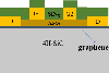
The front view of the device is shown in Fig. 1, graphene active region is between the dielectric layer AI2O3 and the substrate. The graphene substrate is 4H-SiC with a thickness of 500 µm, the source-drain, and two top-gate metal electrode uses Ti/Au (5/95 nm) alloy, the dielectric layer Al2O3 the waveguide SiNx(120 nm).
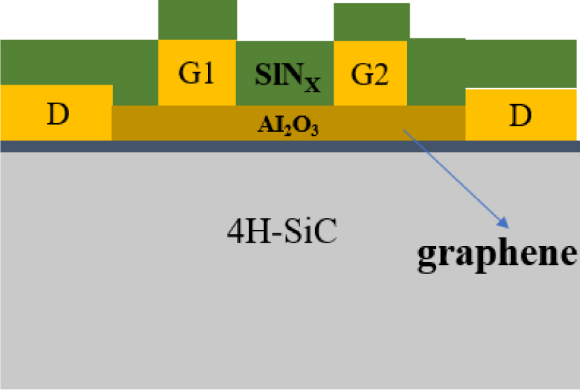
Figure 1: Front view of DBR-DG-GFET.
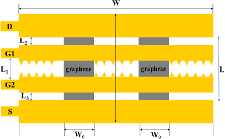
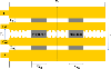
Figure 2: Top view of DBR-DG-GFET.
The top view of the device is shown in Fig. 2, graphene dimensions and the effect of graphene dimensions are as follows:
(1) Since only the zero-gap graphene can stably radiate terahertz photons, the graphene thickness must be 0.34 nm for a single layer.
(2) The total graphene length L is 260 µm, the distance between electrodes L1= L2 = 15 µm. The real impact on the output power is the length of the resonant cavity active region L1. The smaller the gate gap L0 the better but we set it to 30 µm due to the limitation of O2 plasma etching.
(3) Graphene width W0 is set as 100 µm. This value is influenced by the integration and fabrication process and is mainly determined by the design of the resonant cavity target
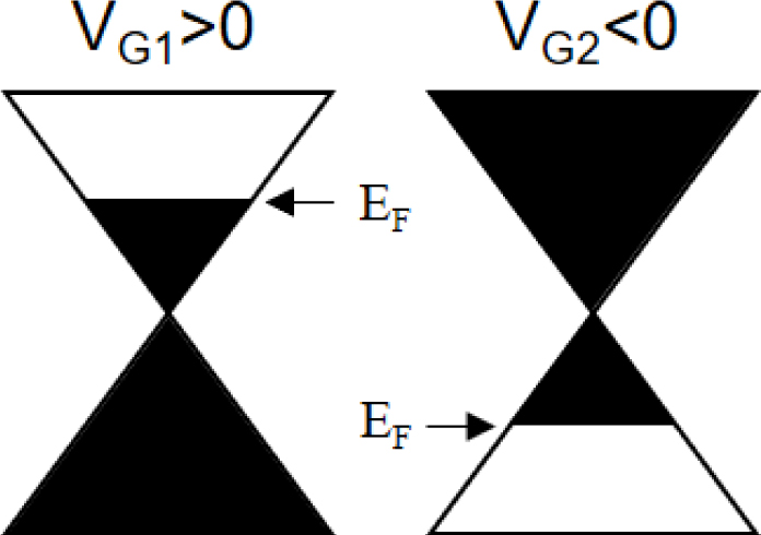
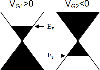
Figure 3: Modulation of the Fermi energy level of graphene by a gate pressure.
Figure 3 illustrates the Fermi energy level of graphene changes due to the gate voltage. With the positive gate voltage attracting electrons, the Fermi energy level moves upwards; The negative gate voltage attracts holes, so the Fermi energy level moves downwards, forming a p-n junction.
3 THEORETICAL CURRENT MODEL OF DG-GFET
Modeling the empirical channel current of the GFET helps us to analyze its electrical characteristic [16, 17]. Theoretical calculations are performed using GCA [17, 18] to clarify the operating mechanism of the DG-GFET under electrical injection.
With the source grounded, V and V are the gate voltages, and the forward bias voltage V is applied to the drain. Figure 4 shows a simplified device area containing only the insulating layer, metal gates, and channel, and the curve is the voltage drop along the channel. Both electrons and holes in DG-GFETs have the potential to become carriers due to the bipolar electric field effect of graphene, which is different from silicon-based transistors.
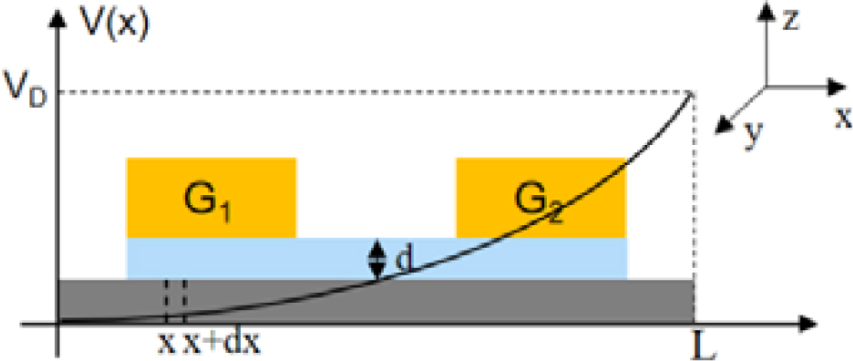
Figure 4: Voltage distribution in the channel.
Where x is the length of a position in the channel area at x, the conductivity . is the number of electrons or holes per unit area. is the charge per unit area, L and W are the length and width of the channel, respectively. The carrier mobility defaults to a fixed value , the conductance at a point in the channel
| (1) | |
where is the amount of charge stored per unit area at x, is the capacitance per unit area at the channel with , and is the insulation dielectric constant and vacuum dielectric constant, respectively. d is the insulation thickness, where V(x) is the bias voltage between x and the source. When the voltage varies on each dx, the microscopic expression for the drain current in the channel is
| (2) |
then integrate from the source (x=0, V(x)=0) to the drain (x=L, V(x)=V) [19]
| (3) |
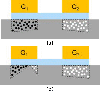
As shown in Fig. 5 (a), if 0 V V, V = 0, the conducting carriers consist of two parts, the side near the source is electron accumulation, and from the source to the drain, the electron concentration gradually decreases to zero, and gradually turns to hole accumulation. Therefore, the drain current is superimposed by the drift of electrons (represented by black spheres) and holes (represented by white spheres) under the action of the drain voltage. Equation (3) is integrated by removing the absolute value and dividing it into two definition domains:
| (4) | |
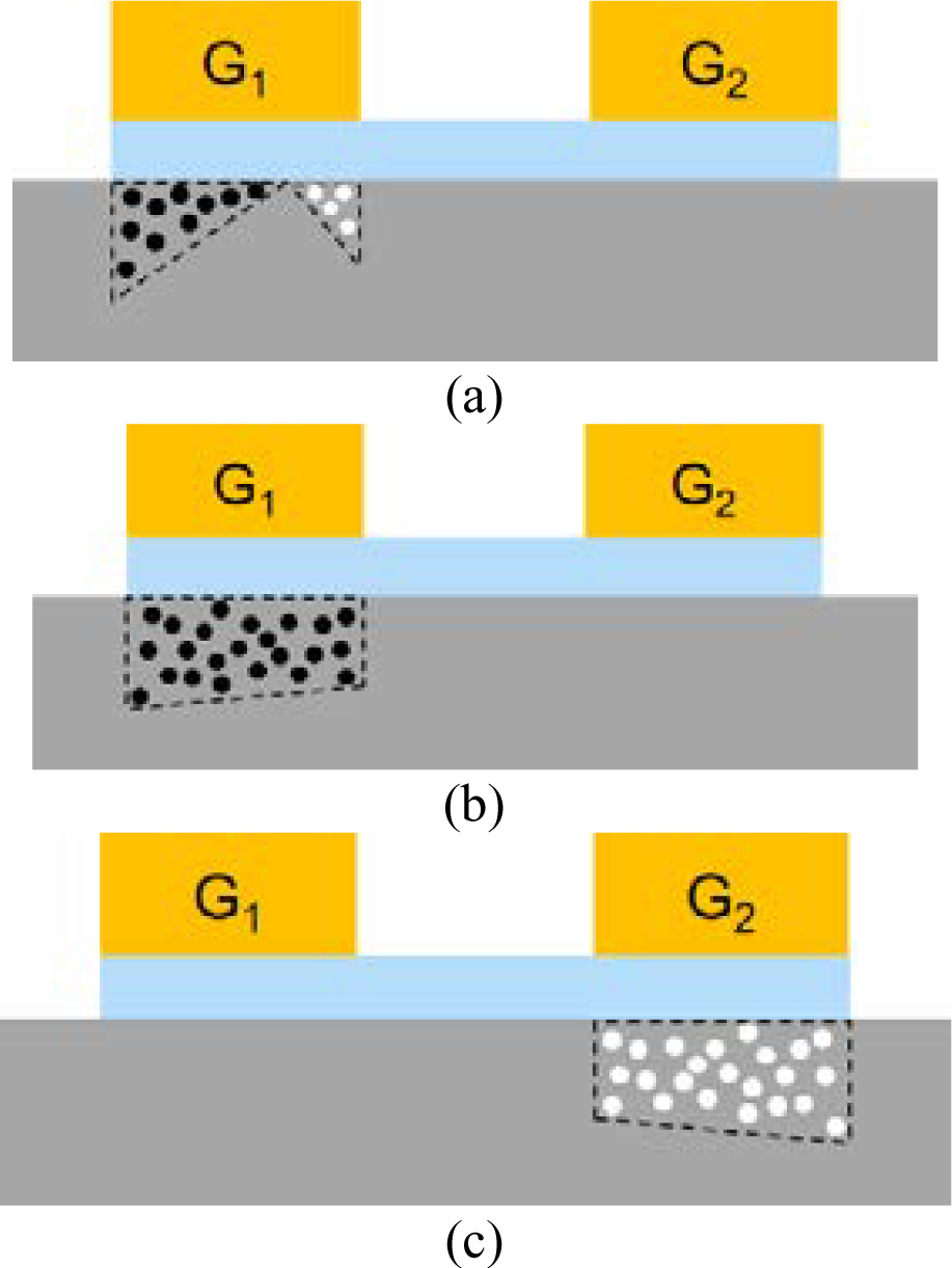
Figure 5: Three carrier distributions for single gate applied pressure (a) 0VV, V=0 (b) VV, V=0 (c) V0, V=0.
In Fig. 5 (b), if the conditions V V and V = 0 are satisfied, the conducting carriers in the channel are mainly electrons, and the operating mechanism is primarily electron conduction when the voltage is applied at the drain. In Fig. 5 (c), if V 0, V = 0, the conducting carriers in the channel are mainly holes, and the operating mechanism is primarily hole conduction:
| (5) |
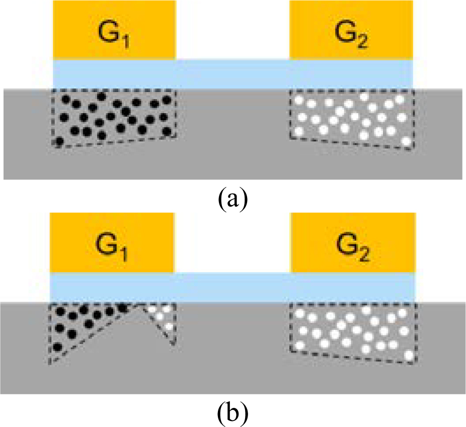
Figure 6: Two carrier distributions for double gate applied pressure. (a) V|V. (b) 0|V|V.
As shown in Fig. 6 (a), when positive and negative voltages of the same magnitude are applied to the two top gates, and the absolute value of the gate voltage is greater than the drain voltage, electrons accumulate in the positive gate voltage region and holes accumulate in the negative gate voltage region. As shown in Fig. 6 (b), when positive and negative voltages of the same magnitude are applied to the two top gates, and the absolute value of the gate voltage is smaller than the drain voltage, electrons accumulate under the positive gate voltage region near the source. In contrast, holes accumulate under the positive gate voltage region near the drain and the negative gate voltage region. Referring to equation (3), the case is divided into two definition domains, and the integration is obtained as follows.
The channel resistance of each segment is
| (6) |
The formula for I is
| (7) |
We get:
| (8) |
where .
The device parameters are set as follows: 2O3), W=400 µm, L=60 µm, =10000 cm/V s, µ=4000 cm/V s, =8.85*10F/cm, d=40 nm
| (9) |
By bringing t and k into equations (5) and (8), the operating current can be calculated for different gate voltage and bias voltage conditions, and the current characteristics of the device are plotted by Matlab.
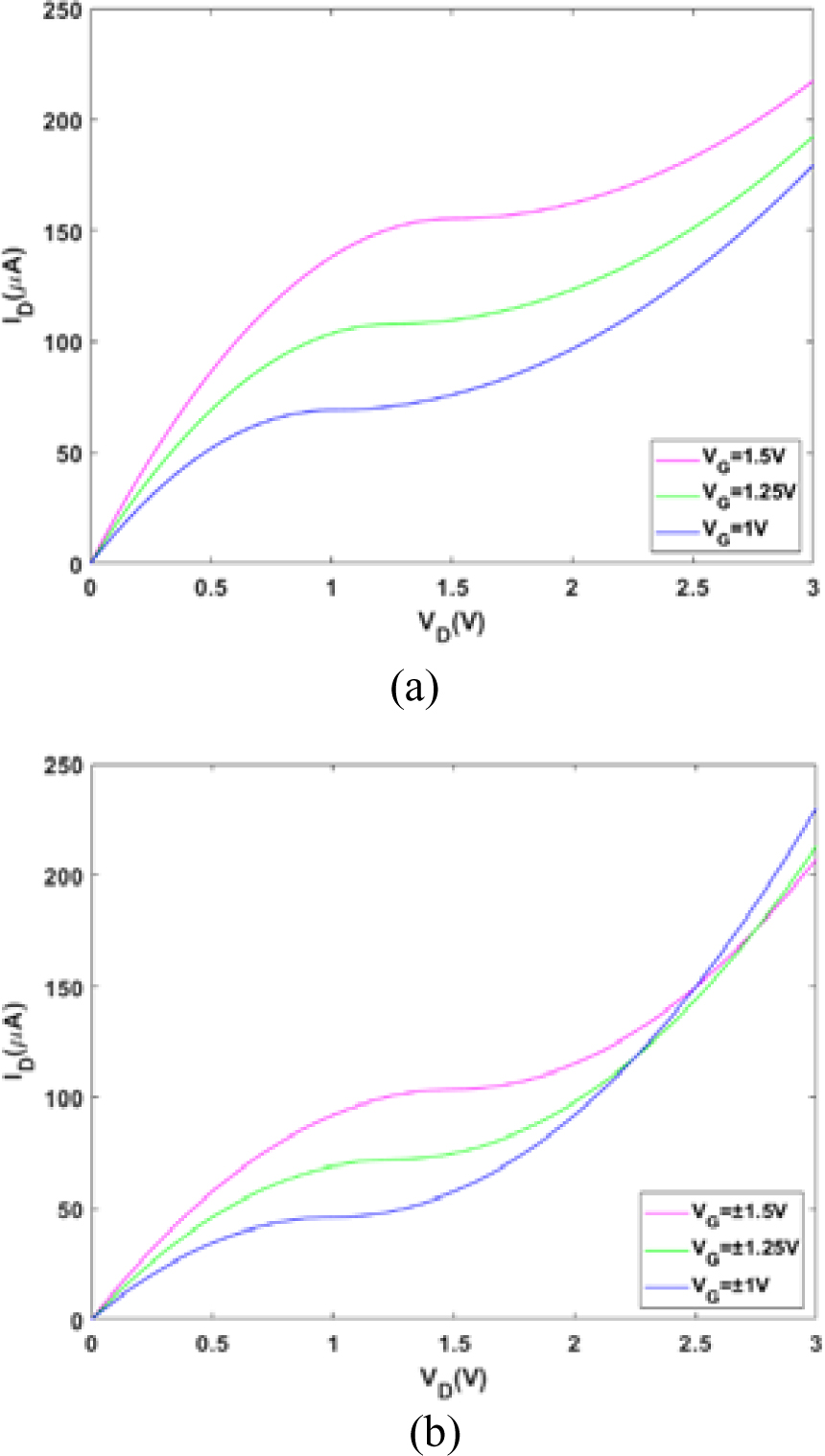
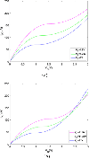
Figure 7: I-V Output characteristic curve. (a) Single-gate applied voltage. (b) Double-gate applied voltage.
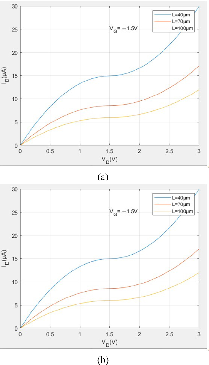
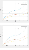
Figure 8: I-V Double gate output characteristic curve under, (a) different channel lengths L, and (b) different k.
Calculations explain the working mechanism of the device. Figure 7 (a) shows the output characteristic curve of the device under the single gate applied voltage. Positive gate voltage induces graphene to form an n-type semiconductor, and electrons accumulate in the channel area. When the drain-source bias voltage is small, electrons move toward the channel anode direction, creating a drift current, corresponding to the first linear region in the figure. As V gradually increases to a critical value, the drift of holes in the channel cannot be neglected. It moves in the opposite direction of electrons, preventing the increase of current, corresponding to the saturation region in the figure. When V exceeds the critical value, the hole conductivity in the channel prevails, and the conductivity type of the channel changes from n-type to p-type, corresponding to the second linear region in the figure. Figure 7 (b) shows the output characteristic curve of the device under the double gate applied voltage, the positive gate pressure induces the accumulation of electrons in the graphene channel region, and the negative gate pressure induces the proliferation of holes in the graphene channel region, and the graphene p-n junction is formed in the channel region. When V is small, electrons move toward the positive pole, and holes move toward the negative. Because the electron mobility is much larger than the hole mobility, the channel still shows electron conduction. Still, the magnitude of the current is reduced compared to the single gate voltage, which reflects the weakening effect of the electric field built into the p-n junction on the drift current. Observe that a transient saturation region arises when the V gradually increases, and the conduction effects of electrons and holes are equivalent at this time; It is worth noting that when V increases to a certain level, a negative transconductance phenomenon occurs, indicating that the gate loses control of the current, which may be because a large gate voltage establishes a higher p-n junction barrier and suppresses the increase in output current.
According to equation (8), the parameters L and k=µ/µ were also simulated to provide a reference for future improvements to the DG-GFET. Figure 8 (a) tells us that the channel length L should be reduced as much as the process can achieve. Figure 8 (b) illustrates that when considering graphene doping, increasing the k value helps to improve the performance of the device
4 DEVICE FABRICATION AND TESTING OF DEVICE
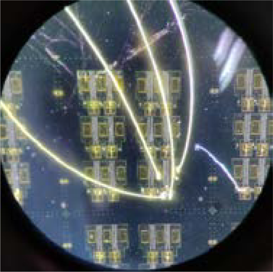
Figure 9: Physical view of the device under a 30 microscope.
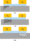
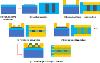
The device is observed under a 30 times microscope, as shown in, as shown in Fig. 9, and four gold wires are connected to the device’s drain, source, and gate pins. The overall fabrication flow of the device is shown in Fig. 10, here are the details [20, 21]:
(1) Obtain monolayer graphene by thermal decomposition of 4H-SiC under low pressure and high-temperature environment using the epitaxial growth method.
(2) Cutting off the excess part of graphene, leaving only the graphene layer in the target region.
(3) Fabrication of leaky and source metal electrodes with Ti/Au material, mainly with process steps of gluing, exposure, development, metal deposition, and exfoliation.
(4) Deposition of Al2O3 media on graphene by atomic layer deposition (ALD), the ALD process allows precise control of the deposition thickness and high quality with fewer impurities.
(5) Growing two top gates with the same Ti/Au material, same steps as (3), it should be noted that the grating is attached to the gate and the size is small, requiring high precision, so a high level of the fabrication process is required.
(6) Deposition of waveguide material SiNx using plasma-enhanced chemical vapor deposition (PECVD) as the cavity material of the resonant cavity and coating on the device output port to improve the device output efficiency.
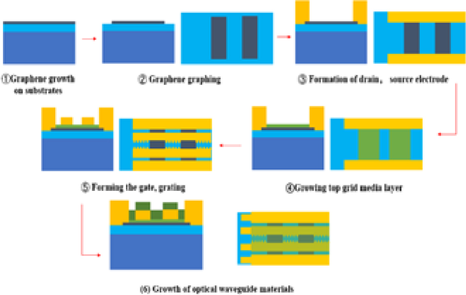
Figure 10: DBR-DG-GFET fabrication steps.
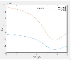
The potential difference between the gate and graphene determines the density of the two carriers in the device channel and whether the conducting type is electrons or holes. A sizeable forward gate voltage leads to the accumulation of electrons in graphene to produce an n-type channel. A sizeable reverse gate voltage leads to the accumulation of holes in graphene to build a p-type channel. This feature forms two branches separated by a Dirac point. After fabrication, electrical tests were performed on the double-top gate GFET. To obtain its transfer characteristic curve, the gate voltage V= -3V-3 V, V=0 V, and the drain-source V were 0.1 V and 0.2 V, respectively, to get its transfer characteristic curve, as shown in Fig. 11. The Dirac point of the intrinsic graphene is located at 0 V, and a bipolar curve shifted to the right is obtained because the substrate is heavily doped silicon, and the Dirac point is situated near 1.8 V, indicating that the graphene channel is P-type doped.
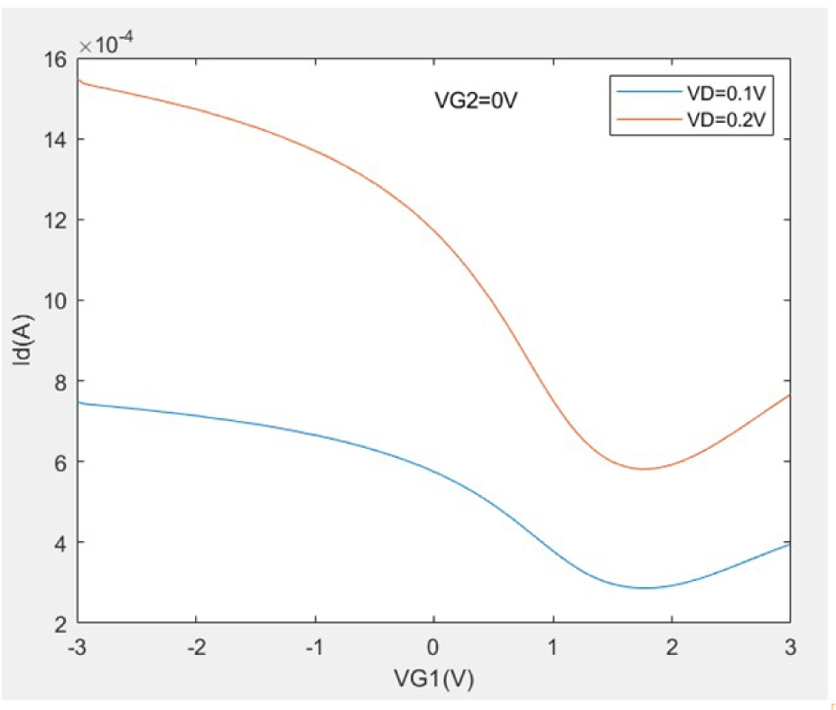
Figure 11: Transfer characteristic test curve.
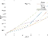
To eliminate the effect of graphene P-type doping, the value of the applied positive gate voltage needs to be greater than the Dirac point so that N-type graphene can be induced below this gate, thus forming a p-n junction. The output characteristics are tested by applying an appropriate forward drain voltage. Let V be 1 V and V be 3 V, 4 V, 5 V, and 6 V, and try the output characteristic curve of the device at the drain-source voltage V from 0 to 5 V Results are shown in Fig. 12.
Based on the results, when no gate voltage is applied, i.e., V=V=0 V, the graphene in the channel region is a good conductor, and the V-I curve is linear, as shown by the dashed line in Fig. 12. If there is no drain voltage, i.e., V=0, the p-n junction is in equilibrium, the current is zero, and the balance is broken after the drain bias is applied; When V gradually increases to the critical point of the p-n junction barrier, the growth trend of current turns; When V exceeds the breakdown point of the p-n junction barrier, the current increases significantly and enters into another linear growth region. It is worth mentioning that when V increases to a certain degreea negative transconductance phenomenon appears, which is due to the large gate voltage establishing a higher p-n junctionbarrier, resulting in a lag in the growth turning point of output current. Overall, the experimental results demonstrate that applying an external bias voltage to the double-top gate device effectively induces graphene to form a p-n junction.
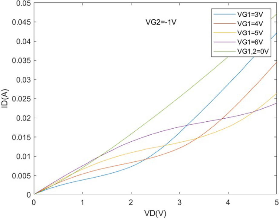
Figure 12: Output characteristics test curve.
5 RESULTS AND DISCUSSION
This paper designs and fabricates a graphene p-n junction device with a double-top gate structure. Comparing experimental test data versus simulation results, the default channel in simulation is pure graphene. The Dirac point is located at 0 V The gate voltage injection is positive and negative with equivalent absolute values. The actual device has a Dirac point shift in the graphene leading to a difference in the gate voltage setting. The measured data are consistent with the simulation results. When the injected bias voltage is small, larger the gate voltage causes the graphene channel to accumulate more non-equilibrium carriers, at which time the current operating increases linearly with the rise of the gate voltage; when the bias voltage is raised to the critical point of breaking through the p-n junction barrier, the trend of current growth turns; When the bias voltage reaches the p-n junction barrier-breaking point, the current starts to increase significantly and enters into the faster linear growth region. A large gate voltage will increase the barrier height of the p-n junction to a certain extent, and the negative transconductance phenomenon appears, which suppresses the continuous increase of the current. Since simulation parameters are less accurate than in perfect theoretical conditions, there are some numerical errors, but overall the model is quitereliable.
ACKNOWLEDGMENT
This work is supported by National Natural Science Fund (61871442), Ministries Fund (6142601200504, 2020-JCJQ-JJ-3 97) funding.
REFERENCES
[1] S. Masuminia, C. Ghobadi, J. Nourinia, M. Karamirad, and B. Mohammadi, “A novel tunable graphene based terahertz absorber with polarization insensitive,” Applied Computational Electromagnetics Society (ACES) Journal, vol. 31, no. 12, pp. 1439-1444, 2021.
[2] B. Beiranvand and A. S. Sobolev, “A proposal for a multi-functional tunable dual-band plasmonic absorber consisting of a periodic array of elliptical grooves,” J. Opt., vol. 22, Art. no. 105005, 2020.
[3] B. Beiranvand, A. S. Sobolev, and A. Sheikhaleh, “A proposal for a dual-band tunable plasmonic absorber using concentric-rings resonators and mono-layer graphene,” Optik, vol. 223, Art. no. 165587, 2020.
[4] V. Kumar, “24 GHz graphene patch antenna array,” Applied Computational Electromagnetics Society (ACES) Journal, vol. 34, no. 5, pp. 676-683, 2019.
[5] S.-l. Wang, J.-S. Hong, Y. D., and Z.-j. Chen, “A frequency reconfigurable antenna based on few layer graphene,” Applied Computational Electromagnetics Society (ACES) Journal, vol. 36, no. 5, pp. 542-547,2021.
[6] R. Bala, R. Singh, A. Marwaha, and S. Marwaha, “Wearable graphene based curved patch antenna for medical telemetry applications,” Applied Computational Electromagnetics Society (ACES) Journal, vol. 31, no. 5, pp. 543-550, 2021.
[7] R. Sordan, F. Traversi, and V. Russo, “Logic gates with a single graphene transistor,” Appl. Phys. Lett., vol. 94, Art. no. 073305, 2009. Available: https://doi.org/10.1063/ 1.3079663.
[8] A. Das, S. Pisana, B. Chakraborty, S. Piscanec, S. K. Saha, U. V. Waghmare, K. S. Novoselov, H. R. Krishnamurthy, A. K. Geim, A. C. Ferrari, and A. K. Sood, “Monitoring dopants by Raman scattering in an electrochemically top-gated graphene transistor,” Nat. Nanotech, vol. 3, pp. 210-215, 2008.
[9] P. Weis, J. L. Garcia-Pomar, M. Höh, B. Reinhard, A. Brodyanski, and M. Rahm, “Spectrally wide-band terahertz wave modulator based on optically tuned graphene,” ACS Nano, vol. 6, no. 10, pp. 9118-9124, 2012.
[10] I. Maeng, S. Lim, S. J. Chae, Y. H. Lee, H. Choi, and J.-H. Son, “Gate-controlled nonlinear conductivity of Dirac Fermion in graphene field-effect transistors measured by terahertz time-domain spectroscopy,” Nano Lett., vol. 12, no. 2, pp. 551-555, 2012.
[11] L. Valentini, J. M. Kenny, F. Alimenti, and L. Roselli, “Planar MOSFET devices on paper substrate using graphene oxide film as gate dielectric,” in Proc. 2013 European Microwave Conference, pp. 5-8, 2013, doi: 10.23919/EuMC.2013.6686576.
[12] J. S. Moon, D. Curtis, S. Bui, T. Marshall, D. Wheeler, I. Valles, S. Kim, E. Wang, X. Weng, and M. Fanton, “Top-gated graphene field-effect transistors using graphene on Si (111) wafers [J],” IEEE Electron. Device Lett., vol. 31, no. 11, pp. 1193-1195, 2010.
[13] J. S. Moon, D. Curtis, M. Hu, D. Wong, C. Mcguire, P. Campbell, G. Jernigan, J. Tedesco, B. VanMil, R. Myers, Jr. Eddy, and D. K. Gaskill, “Epitaxial-graphene RF field-effect transistors on Si-face 6H-SiC substrates,” IEEE Electron. Device Lett., vol. 30, no. 6, pp. 650-652, 2009.
[14] K. Tamersit, “An ultra-sensitive gas nanosensor based on asymmetric dual-gate graphene nanoribbon field-effect transistor: Proposal and investigation,” J. Comput. Electron., vol. 18, no. 3, pp. 846-855, 2019.
[15] J. P. Liu, S. Safavi-Naeini, and D. Ban, “Fabrication and measurement of graphene p–n junction with two top gates,” Electron. Lett., vol. 50, no. 23, pp. 1724-1726, 2014.
[16] J. Sarker and A. Shifat, “An analytical approach for modeling of a top gated graphene based MOSFET[C],” in Proc. Int. Conf. Comput. Inform. Technol., IEEE, 2017.
[17] S. Bardhan, M. Sahoo, and H. Rahaman, “Empirical drain current model of graphene field-effect transistor for application as a circuit simulation tool,” IETE J. Res., no. 3, pp. 1-13, 2019.
[18] M. Weis, “Gradual channel approximation models for organic field-effect transistors: The spacecharge field effect,” J. App. Phys., vol. 111, Art. no. 054506, 2012.
[19] B. Su, J. Huang, and J. Liu, “Current characteristics of double-top-gated graphene field effect transistor,” in Proc. 2021 IEEE 4th Int. Conf. Autom. Electron. Electr. Eng. (AUTEEE), Shenyang, China, Nov. 19-21, pp. 264-267, 2021.
[20] A. Greene, S. Madisetti, P. Nagaiah, V. Tokranov, M. Yakimov, R. Moore, and S. Oktyabrsky, “InGaSb MOSFET channel on metamorphic buffer: Materials, interfaces and process options,” in Proc. 223th ECS Meeting, 2013.
[21] P. D. Ye, A. T. Neal, T. Shen, J. J. Gu, M. L. Bolen, and M. A. Capano, “Atomic-layer-deposited high-k dielectric integration on epitaxial graphene,” ECS Trans., vol. 33, no. 3, pp. 459-466, 2010.
BIOGRAPHIES

Jinbao Huang born in 1999, a native of Luan, Anhui Province, China.
He is a master’s student at the School of Electronic and Optical Engineering, Nanjing University of Science and Technology. His main research interests are terahertz devices.

Yun Wu works in Science and Technology on Monolithic Integrated Circuits and Modules Laboratory, Nanjing Electronic Device Institute. His main research interests are terahertz devices.

Bo Su born in 1997, a native of Xi’an, China.
He got his master’s degree in Optical Engineering from Nanjing University of Science and Technology. His main research interests are terahertz devices.

Jingping Liu School of Electronic and Optical Engineering, Nanjing University of Science and Technology, Nanjing, People’s Republic of China
Her main research areas are antenna design, signal reception, processing, electronic countermeasure technology, and terahertz devices.
ACES JOURNAL, Vol. 37, No. 7, 774–781.
doi: 10.13052/2022.ACES.J.370704
© 2022 River Publishers