A New Approach of Applying Chebyshev Distribution of Series Fed Microstrip Antenna Array for Radar Applications
Mohammed S. Salim, Tareq A. Najm, Qusai Hadi Sultan, and Adham M. Saleh
Department of Communications Engineering, Ninevah University, Mosul, Iraq
mohammed.salim@uoninevah.edu.iq, tareq.najm@uoninevah.edu.iq, qusai.sultan@uoninevah.edu.iq, adham.saleh@uoninevah.edu.iq
Submitted On: April 20, 2022; Accepted On: September 23, 2022
Abstract
In this paper a new method of applying Chebyshev distribution for series fed antenna array was proposed for radar applications. The first part of this study consists of applying the proposed method on antenna arrays working at 2.3 GHz (S-band radar applications) with 6, 8, 10, 14, and 28 elements, whereas the second part of the study is applying the method on antenna arrays working at 5.2 GHz (C-band radar applications) with the same number of elements. The achieved sidelob level is around (19.6- 24 dB).The obtained antenna gain is around (10-17.4 dB) depending on the number of elements. Whereas the horizontal half-power beam width is around (7 – 20).
Index Terms: Antenna array, Chebyshev distribution, series fed, side lob level.
I. INTRODUCTION
Radars can be used in many fields such as marine applications, air traffic control, and military fields. There are many frequency bands dedicated to radar applications, for example, X-band (8.5-10.5 GHz), S-band (2.3-2.38 GHz), and C- band (5.2-5.8 GHz) [1].
In general, antennas play a significant role in radar systems and they affect the performance of the radar systems. There are many types of antennas used in radars applications such as parabolic antennae, horn antennae, and microstrip antennae. The accuracy of radar detection depends on several antenna parameters for instance side lobe level, HPBW, polarization, and gain. Microstrip antenna arrays are widely used in radar applications, due to their unique features such as high gain, low cost, lightweight, and low profile, and can accurately control the radiation patterns [2]. The desired radiation pattern of the antenna array can be formed depending on the spacing between the elements. It is also relying on the excitation’s distribution of the elements. The most popular methods of amplitude distribution are uniform, Chebyshev and Binomial distribution. Feeding of microstrip patch antenna array can be achieved by single feed or multiple ports. Because of the simplicity of a single feed port, it is widely used in radar antennas. Chebyshev method was chosen to apply to the series feed array antenna with single.
Reducing the side lobe of antenna arrays has attracted much research in recent years [3–8]. Designing a series-fed microstrip array antenna for x-band Indonesian maritime radar was proposed by Hajian M. et al. In the mentioned work, the researchers designed an 8- and 16element antenna array and they used the spacing between elements as a parametric study to optimize the radiation pattern [9]. Chen Z. and Otto S. studied a taper optimization of a microstrip patch antenna array [10]. A 2*16-element antenna array working at 9.35 GHz for marine radar applications were proposed by Kuo F. Y. and Hwang R. B. [11]. The researchers used s-parameter analysis to find the values of main feed line impedances by which the Chebyshev distribution is achieved [11]. Milijić M. et al studied the influence of feeding structure on the side lobe level [12]. A 4*4 non-uniform antenna array working at 0.9 GHz was designed by Inserra D., Hu W., and Wen G. They used a sequentially rotated series power divider to apply a Chebyshev tapering [13]. Toan, Tran, and Giang proposed a double-sided printed dipole linear array antenna working at 5.5 GHz for WLAN outdoor applications. The proposed antenna consists of 10- element double side; also the researchers used series-fed Chebyshev tapering [14].
The main idea behind this paper is to examine a new analysis method to apply Chebyshev distribution for a series-fed microstrip antenna array. The distribution of amplitude excitations of the array elements is controlled by changing the width of the main feed line. The variation of the width was evaluated depending on the impedance values, which were calculated by the proposed method. By applying this method of analysis, a wider feed line was obtained as compared to other works. This technique allows more power to be transmitted through the antenna array due to the fact that impedance values are reduced with increasing the width of the feed line. In addition, the increased width of the feed lines is an advantage from the manufacturing perspective since less fabrication accuracy is needed. Furthermore, the proposed method in this work has shown that the variation of the feed line’s impedance is too small where the impedance values are ranging from 43 to 70 , which in fact doesn’t necessitate the use of /4 transform. All these advantages of the proposed technique cause the proposed antenna arrays to exhibit low complexity and low fabriction cost in addition to handling higher power while maintaining the standard acceptable performance.
II. THEORETICAL ANALYSIS
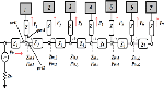
The analysis of the feeding network was achieved by considering each feed line of the elements as a tee junction, which is denoted by T1, T2….T6 as shown in Fig. 1, [11]. The distance between the two elements was chosen to be one wavelength , whereas the length of the feeding line of each element is /4 see Fig. 1. The power ratio between the tee junction ports is depending on the characteristic impedance of the microstrip lines. The impedances of the main feed line are denoted by Zi, where i = 1, 2…7 as explained in Fig. 2. The value of Z was assumed to be 70 . The impedances of the feed lines of all the elements were assumed to be the same and denoted by Z = 50 except element 7, which was assumed to be 45 . The values of Zto Zwhich represent the impedances seen after i-th tee junction were calculated depending on the power divider relation. For example, to calculate Z, at tee junction 1 the power divider relationship is given by [13]:
| (1) |
Where: P is the total power fed to the one side of the feeding network. P is the power delivered to port 2 of the first tee junction and it is given by Eq. 2.
| (2) |
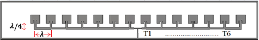
Fig. 1: The proposed antenna array configuration (14 elements).
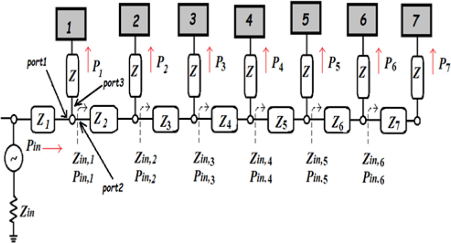
Fig. 2: Equivalent circuit of the right side 14-element antenna array.
Where P, P……. P is the power fed to each element of the array, which was calculated according to the Chebyshev distributions. Therefore, the values of Zto Z were evaluated using Eq. 1. To calculate the values of Z, a reverse impedance analysis was applied. The values of the calculated Z are listed in Table 1. Depending on the assumed values of Z and Z, the obtained range of Z is extended from 43 to 70 . On the other hand, this assumption excludes the use of /4 transform between the elements but only one /4 transform is used in the feed that separates both sides of the antenna array.
Table 1: Values of calculated impedances of the main feed line
| Impedance | Value of the Impedance | Width of the Line (mm) |
|---|---|---|
| (assumed) | 70 | 1.5 |
| 49.5 | 3 | |
| 51.1 | 2.85 | |
| 51.7 | 2.8 | |
| 52.5 | 2.7 | |
| 61 | 2.04 | |
| 43 | 3.8 |
III. ANTENNA DESIGN
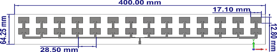
Fig. 3: Geometry of the 214-element antenna array at C-band.
A rectangular microstrip antenna was chosen to be the basic element of the array. The width (W) and length (L) of the elements were optimized to satisfy the desired frequency bands. At the S-band, the dimensions of the patch antenna is W = 39.18 mm and L = 30.4 mm, whereas W = 17.1 mm and L = 12.8 mm at the C-band.
Table 2: Calculated Chebyshev amplitude excitation
| Amplitude Excitation of the i-th Element | 6 Elements |
8 Elements |
10 Elements |
14 Elements |
| a | 1 | 1 | 1 | 1 |
| a | 0.72 | 0.818 | 0.89 | 0.786 |
| a | 0.37 | 0.544 | 0.706 | 0.496 |
| a | —— | 0.33 | 0.485 | 0.266 |
| a | —— | —— | 0.357 | 0.138 |
| a | —— | —— | —— | 0.077 |
| a | —— | —— | —— | 0.0065 |
At the beginning, a 14-element antenna array working on 2.3 GHz was designed. The array is divided into two symmetrical parts each part contains 7 elements as shown in Fig. 1. The proposed antenna array was implemented on FR4 substrate with relative dielectric constant = 4.3, thickness of 1.6 mm and tangent loss = 0.025.
The feeding network was designed according to the Chebyshev distribution. The amplitude excitation of each element was calculated based on the Chebyshev method [1] and listed in Table 2. To validate the proposed method of feeding network analysis, two steps were applied. The first step is to change the number of elements (6, 8 and 10) for the proposed antenna array at 2.3 GHz. The second step of validation is to redesign the same antenna arrays (6, 8, 10 and 14 elements) at different frequency band (5.2 GHz). To increase the gain of the array, the number of elements was duplicated as shown in Fig. 3 to be a 214-element antenna array.
IV. RESULTS ANALYSIS
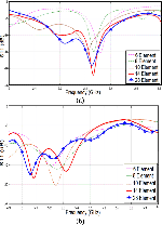
This section presents the simulated results of the proposed antenna arrays in terms of reflection coefficient (S11), surface current distribution, half power beam width (HPBW), antenna gain and sidelobe level at two frequency bands (S and C band). These simulated results are obtained by CST software package. The simulated reflection coefficients for the two arrays are explained in Figs. 4 (a) and (b). Each array is simulated with different number of elements (6, 8, 10, 14 and 28 elements) to show their effect on the bandwidth. It is clear from figures that the obtained bandwidth fluctuated when increasing the number of elements in both bands. These fluctuations can be related to the effect of the feeding network. By increasing the number of elements the feeding network becomes more complex and the overall impedance of the antenna array will change. This will affect the S11 and bandwidth results. Additionally, it can be noticed that there is a small shift in the operating frequency bands. This shift happened because of the change of the total physical length of the array antenna due to the change in the number of elements in eacharray.
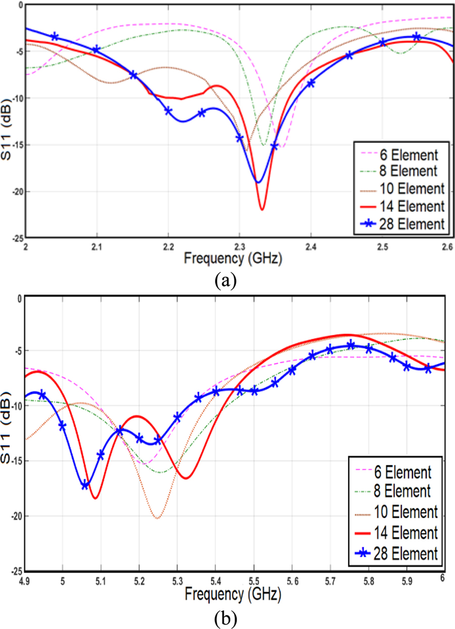
Fig. 4: S11 of the designed antenna arrays at: (a) S-band. (b) C-band.
Furthermore, the 2D-Normalized antenna array patterns in xz-plane were plotted in Fig. 5 while the antenna parameters of the presented antennas like HPBW, antenna gain and side lob level were listed in Tables 3 and 4. These tables show the natural trend of decreasing HPBW with increasing the number of radiating elements in 1-D antenna array [2]. This means compressing the radiation pattern in the xz-plane (horizontal) and expanding the radiation pattern in the yz-plane (vertical). The only exception for the previous scenario is in the case of the 214 element where the horizontal HPBW is slightly increased approximately by 2. This increase is resulted from duplicating the number of elements from 14 to 214 element, which leads to compress the pattern in elevation and expand the pattern in the horizontal plane.
Table 3: HPBW, Gain and SLL of array antennas at 2.35 GHz
| No. of Elements | HPBW (deg.) xz- Plane | HPBW (deg.) yz- Plane | BW(MHz) | Gain (dB) | SLL (dB) |
| 6 | 20.3 | 78 | 44 | 10 | 22 |
| 8 | 19.5 | 79 | 40 | 10.8 | 20 |
| 10 | 17 | 81 | 76 | 11.3 | 23 |
| 14 | 7.4 | 89 | 169 | 14.5 | 20 |
| 2*14 | 9.1 | 86 | 199 | 17.4 | 21.5 |
Table 4: HPBW, Gain and SLL of array antennas at 5.2 GHz
| No. of Elements | HPBW (deg.) xz- Plane | HPBW (deg.) yz- Plane | BW(MHz.) | Gain (dB) | SLL (dB) |
| 6 | 20.4 | 79 | 240 | 10.1 | 19.7 |
| 8 | 20 | 79 | 387 | 10.3 | 19.6 |
| 10 | 13.1 | 82 | 290 | 11.4 | 21.9 |
| 14 | 8.4 | 85 | 408 | 13.2 | 20.1 |
| 2*14 | 10.8 | 83 | 357 | 17 | 23.1 |
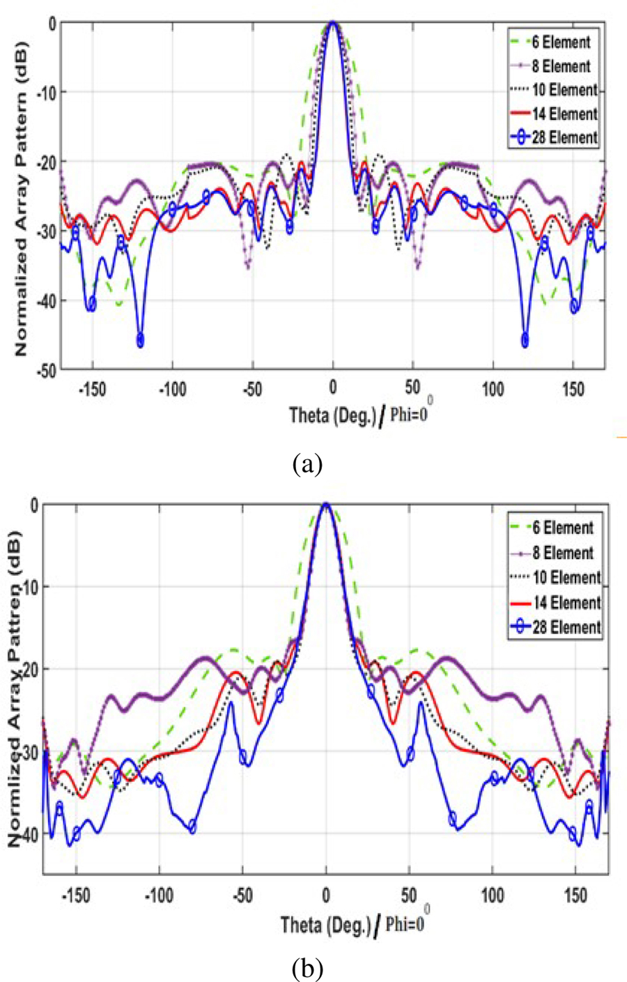
Fig. 5: 2D Radiation pattern in x-z plane of the designed antenna arrays at: (a) 2.35 GHz; (b) 5.2 GHz.
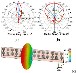
Moreover, the tables indicate that the gain of antenna arrays are increased with increasing the number of elements. A 3dB gain enhancement was obtained by duplicating the radiating elements from 14 to 28. Regarding to the achieved side lob level, it is approximately -19 down to -25 dB. On the other hand, the surface current distribution for the 214-element antenna array is shown in Fig. 6. It evident that the radiating elements at the center of the arrays have higher amplitude excitation compared to the elements at the edges of the arrays as shown in the amplitude excitation values in Table 2. Finally, the 3D and 2D radiation patterns for 28 elements were illustrated in Fig. 7 and Fig. 8 at thetwo bands.
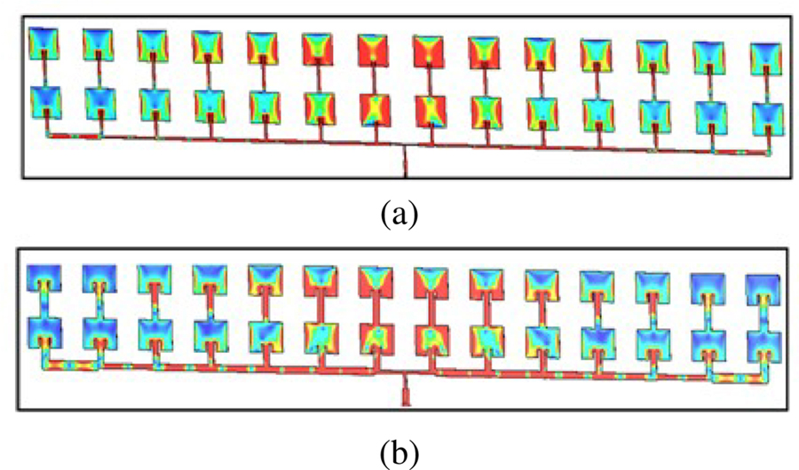
Fig. 6: Surface current distribution of 28 element at: (a) 2.35 GHz; (b) 5.2 GHz.
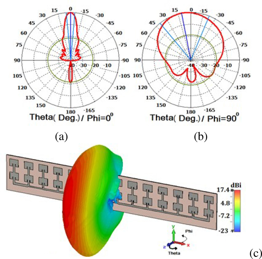
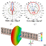
Fig. 7: Far-field radiation pattern of the antenna array at 2.35 GHz.: (a) H-plane; (b) E-plane; (c) 3D pattern.
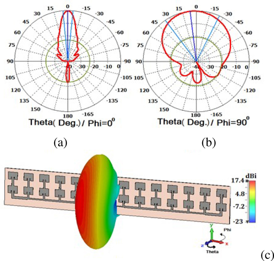
Fig. 8: Far-field radiation pattern of the antenna array at 5.2 GHz: (a) H-plane; (b) E-plane; (c) 3D pattern.
V. EXPERIMENTAL RESULTS
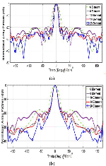
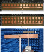
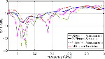
To validate the simulation results, 14 and 28-element prototype antenna arrays at 5.2GHz were created on a PCB board as shown in Fig. 9. A vector network analyzer (VNA) was used to test the S-parameter of the printed antennas. Comparisons between the simulated and measured outcomes for the two proposed antennas are depicted in Fig. 10. It is clear from these comparisons that the results of the 214-element antenna array have the same tendency whereas some differences were noticed in the results of the 14-element antenna array.
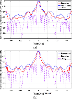
The radiation pattern is another significant parameter that should be tested practically inside the anechoic chamber to show the side lobes levels and compare it with the simulation ones. The x-y plane radiation pattern was plotted. Figure 11 shows the comparison of the x-y plane radiation pattern of the theory with the simulated and measured results. The theory results were obtained using the equations listed in [1]. The array factor was calculated first and then multiplied with the radiation pattern of the single-element antenna. It is clear from Fig. 11 that a good agreement is achieved between simulated and measured results for the two proposed antenna arrays. All the obtained results are summarized in Table 5. It is clear from the table that the experimental results have the same trend as those obtained by simulation with small differences.
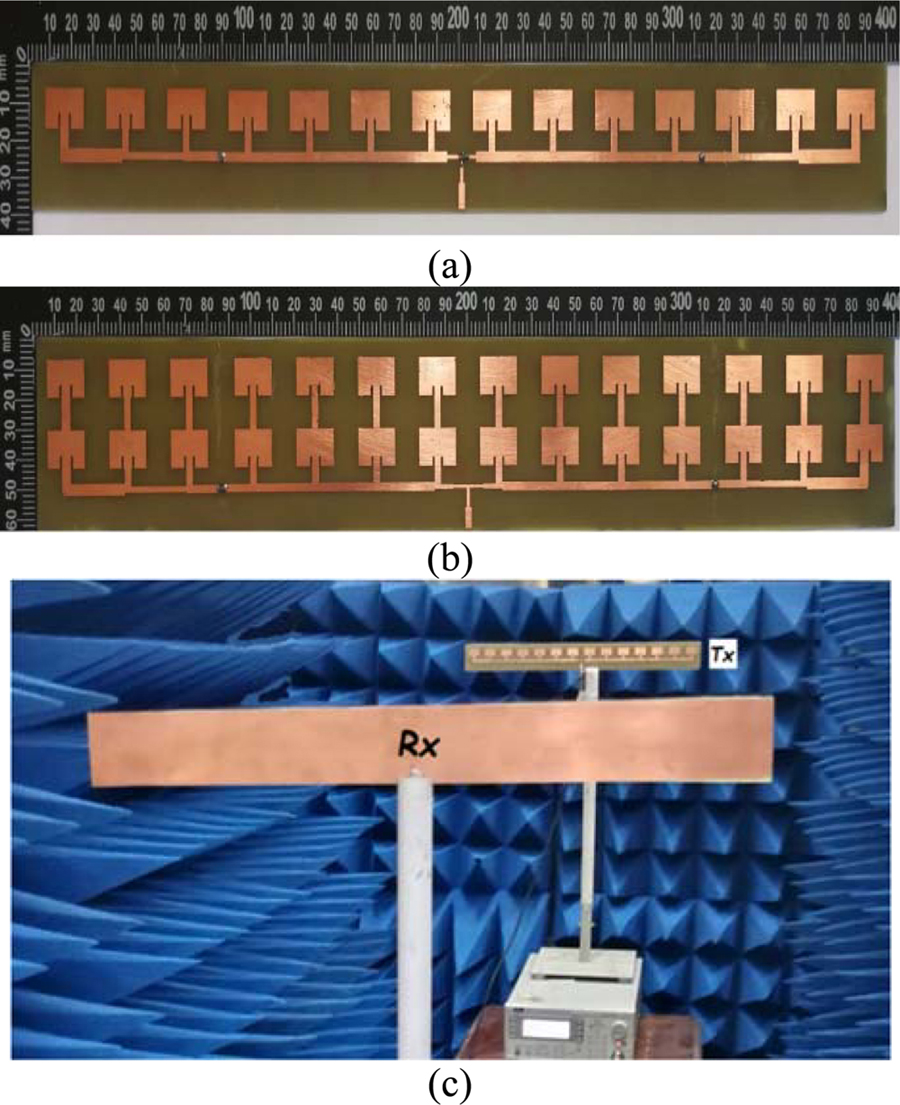
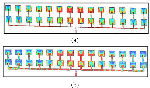
Fig. 9: Fabricated antenna arrays and experimental setup. (a) 14-elements fabricated antenna array. (b) 28-elements fabricated antenna array. (c) experimental setup.
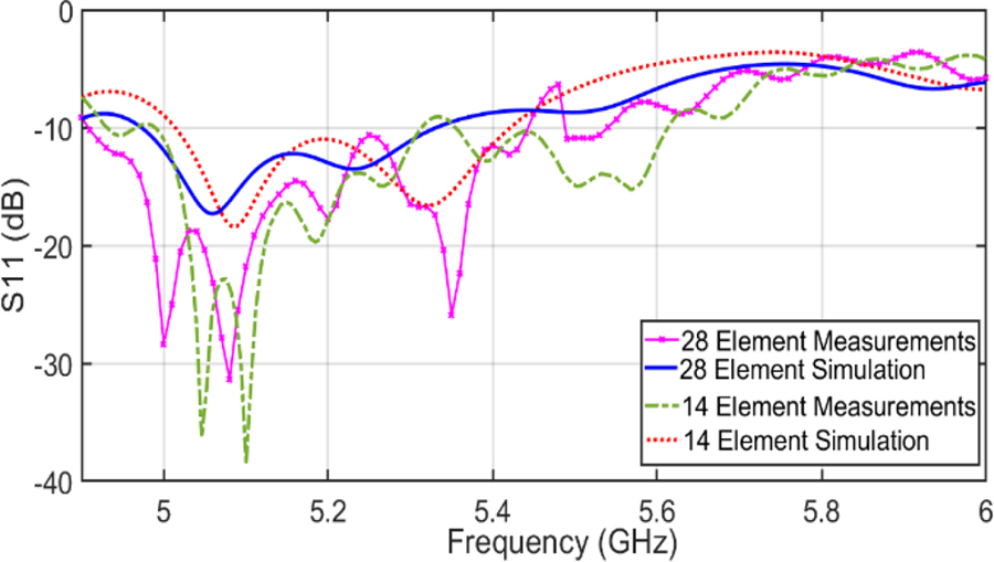
Fig. 10: Comparison of S11 results between Simulation and Measurements at C-band.
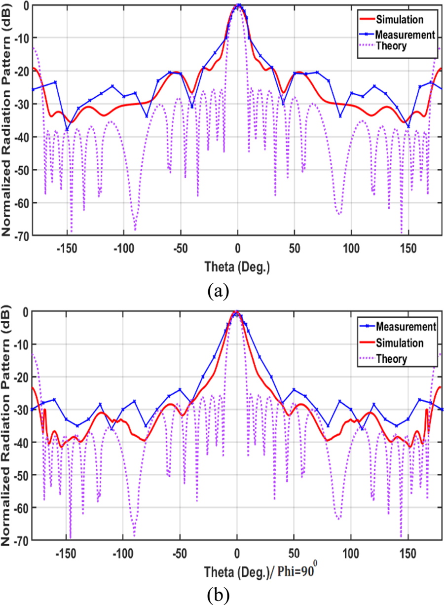
Fig. 11: Comparison of xy-plane results for the printed antenna array at 5.2 GHz. (a) 14-elements. (b) 28-elements.
Finally, the differences between simulation and measurements results in Figs. 10 and 11 can be related to the assumed values of the of the substrate and the effect of non-ideal environment of the Lab. In addition, due to the toleration of manufacturing and soldering, there are some deviations between the measured and simulated data. In general, the proposed antennas have achieved the expected SLL. The differences between the theory against the simulation and measurement results can be related to the fact that the theory does not take into account the effect of mutual coupling between the elements.
Table 5: HPBW, gain and SLL of array antennas at 5.2 GHz of the simulated and measurement results
| No. of Elements | HPBW (deg.) xz plane | BW(MHz) | Gain (dB) | SLL (dB) |
| 14 Simulated | 8.4 | 408 | 13.2 | 20.1 |
| 14 Measured | 12 | 318 | 12.1 | 20 |
| 2*14 Simulated | 10.8 | 357 | 17 | 23.1 |
| 2*14 Measured | 10 | 540 | 15.7 | 24 |
VI. COMPARESION WITH OTHER WORKS
Table 6 shows a comparison between the obtained results of the proposed antenna arrays in this article with other works. To make a fair comparison, the performance of the antenna array was compared with other works in literature that have the same number of elements. It was observed that a good agreement with such works is obtained in terms of HPBW and SLL. However, the values of BW that are obtained in this work outperform other reported works. In addition, there are some differences in gain values, which can be related to the number of elements or to the geometry of the antenna array as shown below. Finally, the overall agreement between the obtained results and the other works validate the proposed method of applying the Chebyshev distribution with gaining the advantage of less complexity and cost.
Table 6: Comparing with results from other works
| This work Sim. | This work Sim. | This work Meas. | [10] | [14] | [11] | |
| No. of Elements | 1*10 | 2*14 | 2*14 | 1*10 | 1*10 | 2*16 |
| Freq/GHz | 5.2 | 5.2 | 5.2 | 5.8 | 5.5 | 9.35 |
| HPBW/0 | 13.1 | 10.8 | 10 | 10 | 10.4 | 5.3 |
| BW/MHz | 290 | 357 | 540 | 90 | 212 | 100 |
| Gain/dB | 11.4 | 17 | 15.7 | —- | 17.5 | 22 |
| SLL/dB | 21.9 | 25.6 | 24 | 20 | 26 | 26.4 |
By comparing the design of 10 elements with a reference [10], a good correlation was observed between the results. In [10], a symmetric 10-element antenna array with a Chebyshev tapering operating at 5.8 GHz has been designed by two methods of tapering. The first is the patch width tapering method and the second is the feed line tapering method [10]. As compared to [14], there is a difference in the results of the SLL and gain for the design of 10-element antenna array at the C-band. The difference of the gain values is due to the effect of the driven element, which is found above each element in the array reported in [14]. Whereas the difference of the SLL can be related to the methodology of the design and the type of the material (Roger RT/Duroid). The main difference between this work and [14] is the methodology of the design. Shunt stubs were added to the main feed line to achieve Chebyshev tapering with calculated values of the impedances of these stubs ranging from 45-178 whereas in this work they are from 43-70 . In addition, in [14] the value of the higher impedance is 178 and the width of the strip line less than 0.8mm, which represent weakness when using high power. In [11] the researchers designed a 2*16-element antenna array. They used the width of the main feed line to achieve the Chebyshev distribution. They considered each junction of the feed line of the element as a tee junction then they found the s-matrix of the tee junction. Depending on the analysis of the s-matrix, they found the impedances of the main feed line. In addition, they considered the impedance value of feed lines of the elements to be equal to 100 . It can be noticed that they use a /4 transformer after each junction. Referring to [11], the SLL results of the design of the 214-element antenna array is approximately equal. On the other hand, the gain values of this work are lower by 5dB. This difference in the gain values is caused by the effect of two metallic plates bounding the antenna array in [11], which acts as a director. It is true that the gain was improved by using such a director, but this gain is at the price of complexity and reliability. Thus, careful consideration should be paid tosuch tradeoffs.
VII. CONCLUSION
A new method of applying Chebyshev distribution on a microstrip antenna array is produced. The method is tested by designing two sets of antenna arrays that work at the S-band and C-band respectively. As mentioned previously, the values of the impedances of the main feed line is around (43-70 ) which means the quarter wavelength transformers are not needed. The feed line of the proposed array is wider than the previous designs of the other researchers, which allows more power to be transmitted through it. The practical measurements show an agreement with the simulation results. The proposed antenna (214 Element) is suggested for radarapplications.
REFERENCES
[1] ITU Recommendation V431-8, “Nomenclature of the frequency and wavelength bands wsed in telecommunications,” Aug. 2015.
[2] C. A. Balanis, Antenna Theory Analysis and Design, 3rd edition, John Wiley & Sons, 2005.
[3] K. H. Sayidmarie and Q. H. Sultan, “Synthesis of wide beam array patterns using random phase weights,” International Conference of Electrical, Communication, Computer, Power and Control Engineering ICECCPCE, vol. 13, pp. 52-57, Dec. 17-18, 2013.
[4] H. Luo, Y. Xiao, W. Tan, L. Gan, and H. Sun. “A W-band dual-polarization slot array antenna with low sidelobe level,” Applied Computational Electromagnetics Society (ACES) Journal, vol. 34, pp. 1711-1718, Nov. 2019.
[5] M. R. Sarker, M. M. Islam, M. T. Alam, and M. H. E-Haider, “Side lobe level reduction in antenna array using weighting function,” International Conference on Electrical Engineering and Information & Communication Technology ICEEICT, Bangladesh, pp. 1-5, Apr. 2014.
[6] J. R. Mohammed and K. H. Sayidmarie, “Sidelobe cancellation for uniformly excited planar array antennas by controlling the side elements,” IEEE Antennas and Wireless Propagation Letters, vol. 13, pp. 987-990, 2014.
[7] H. Singh and S. K. Mandal, “Side lobe levels reduction in digitally optimized time modulatedlinear arrays using particle swarm optimization technique,” Students Conference on Engineering and Systems, India, pp. 1-4, May 2014.
[8] E. Kurt, S. Basbu, and K. Guney, “Linear antenna array synthesis by modified seagull optimization algorithm,” Applied Computational Electromagnetics Society (ACES) Journal, vol. 36, pp. 1552-1562, Dec. 2022.
[9] M. Hajian, J. Zijderveld, A. A. Lestari, and L. P. Ligthart, “Analysis, design and measurement of a series-fed microstrip array antenna for X-Band Indra: the indonesian maritime radar,” European Conference on Antennas and Propagation, Berlin, Germany, pp. 1154-1157, Mar. 2009.
[10] Z. Chen and S. Otto, “A taper optimization for pattern synthesis of microstrip series-fed patch array antennas,” European Wireless Technology Conference, Rome, Italy, Sep. 2009.
[11] F. Y. Kuo and R. B. Hwang, “High-isolation X-band marine radar antenna design,” IEEE Transactions on Antennas and Propagation, vol. 62, no. 5, pp. 2331-2337, May 2014.
[12] M. Milijić, A. Nešić, B. Milovanović, N. Dončov, and I. Radnović, “Feeding structure influence on side lobe suppression of printed antenna array with parallel reflector,” 12th International Conference on Telecommunication in Modern Satellite, Cable and Broadcasting Services (TELSIKS), Nis, Serbia, Oct. 2015.
[13] D. Inserra, W. Hu, and G. Wen, “Design of a microstrip series power divider for sequentially rotated nonuniform antenna array,” International Journal of Antennas and Propagation, vol. 2017, Jan. 2017.
[14] M. T. Nguyen and V. B. Giang Truong, “A novel chebyshev series fed linear array with high gain and low sidelobe level for WLAN outdoor systems.” Applied Computational Electromagnetics Society (ACES) Journal, vol. 34, no. 8, Aug. 2019.
BIOGRAPHIES

Mohammed Sameer Salim was born in Mosul, Iraq in 1987. He received a B.Sc. degree in Communications Engneering in 2007, then completed his M.Sc. study in Ccommuncation Engineering at the College of Electronics Engineering, Ninevah university (2013). Currently, he works as an assistant lecturer at the same collage. His reserch interests include antenna design, antenna arrays, and wave propagation.

Tareq A. Najm was born in Mosul, Iraq, in 1984. He received B.Sc. and M.Sc. degrees from Ninevah University, Iraq in 2006 and 2013, respectively, in Communications Engineering. He has been a Lecturer at Ninevah University since 2013. His current research interests include MIMO antenna design, filter design, ultrawide band antennas (UWB), and multi-band antenna techniques.

Qusai Hadi Sultan was born in Mosul, Iraq, in 1979. He received B.Sc. and M.Sc. degrees from Mosul University, Iraq in 2007 and 2014, respectively, in Communications Engineering. He has been a Lecturer at Ninevah University since 2008. His current research interests include antenna array, reflect antenna array, fractal antenna design, and multi-band antenna techniques.

Adham Maan Saleh was born in Mosul, Iraq, in 1984. He received B.Sc. and M.Sc. degrees from Ninevah University, Iraq in 2006 and 2012, respectively, all in Communication Engineering. After that, he received a Ph.D. degree from the University of Bradford, West Yorkshire, UK, in 2020 in Antennas Engineering He has been a Lecturer at Ninevah University since 2012. His current research interests include MIMO antenna design, defected ground structures (DGS), neutralization techniques, reflectarrayantennas, and multiband antennastechniques.
ACES JOURNAL, Vol. 37, No. 9, 933–940.
doi: 10.13052/2022.ACES.J.370902
© 2022 River Publishers