Complementary Frequency Selective Surface with Polarization Selective Responses
Jian Jiao, Nianxi Xu, and Jinsong Gao
1School of Physics, Changchun Normal University, Changchun 130032, China
xinhe7hl@126.com
2Key Laboratory of Optical System Advanced Manufacturing Technology, Changchun Institute of Optics, Fine Mechanics and Physics, Chinese Academy of Sciences, Changchun 130033, China
xnxlzhy999@126.com
3Jilin Provincial Key Laboratory of Advanced Optoelectronic Equipment and Instruments Manufacturing Technologies, Changchun 130033, China
gaojs@ciomp.ac.cn
Submitted On: October 24, 2020; Accepted On: April 4, 2022
Abstract
This paper reports the design and electromagnetic performance of a new complementary frequency selective surface (CFSS) which shows polarization selectivity and good angular stability. Each CFSS unit cell only consists of a thin substrate sandwiched by a square patch array and its complementary square slot array with lateral displacement. The polarization selectivity of the proposed CFSS is determined by the displacement introduced between two arrays. An equivalent circuit model has been developed for this structure to interpret its polarization selective feature. The CFSS structure has been analyzed with full-wave simulation. The polarization selectivity of the proposed structure was verified by experiment.
Keywords: Frequency selective surface (FSS), complementary screen, polarization selective surface (PSS).
I. INTRODUCTION
Frequency selective surfaces (FSSs) are two-dimensional periodic arrays that have been widely used in a lot of applications, such as various microwave systems and antenna radomes [1, 2]. The FSSs with polarization selective response are called polarization selective surfaces (PSSs). The polarization selectivity is significant to anti-interference performance and detection capability. The PSSs are important in antenna applications and can be used in many fields, such as polarimetric imagining radars and communicationsatellites [3, 4].
There are so many ways to achieve linear polarizer. One classic way is to use parallel metal strip structure [5]. But its bandwidth should be widened by adding more layers. Some other linear polarizers are obtained by well-designed FSS structure [6]. Complementary frequency selective surface (CFSS) has many advantages in designing polarizer, such as good angular stability, low profile, and easy fabrication [7].
In this work, an alternative design of PSS based on CFSS structure is proposed. The PSS consists of a square patch array and a complementary square slot array separated by a thin substrate. An important parameter lateral displacement DSX is introduced. Its geometry and frequency responses are presented and explained from the circuit point of view. The measured transmissions, including normal and oblique incidence, are obtained. It is indicated that the proposed CFSS structure has polarization selectivity and its filtering performance is insensitive to the variation of the incident angle of illuminated wave. Polarization selectivity, low profile, and light weight make it a promising application in metamaterial polarizers on curved surfaces.
II. CFSS DESIGN AND CIRCUIT ANALYSIS SECTION FORMATTING
A. Design description
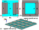
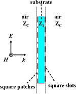
The proposed CFSS has two printed layers separated by a very thin dielectric substrate. On the top surface, there is a 2-D periodic array of metallic square patches, and on the bottom, there is a 2-D periodic array of complementary square slots. Figures 1 (a) and (b) show the unit cell of the proposed CFSS structure and its physical parameters. The period of the unit cell is Dx = Dy = D, and the length of square patch and slot is L. An important parameter, lateral displacement DSX along the x-axis, is introduced. And there is no lateral displacement DSY along the y-axis (DSY = 0) as shown in Figure 1 (a). That means the center of the square patch is shifted by DSX, along the x-axis, relative to the center of the square slot. Here, let DSX = D/2 in this work. Figure 1 (c) shows the 3-D view of the proposed CFSS array. The side view of the proposed CFSS array is shown in Figure 2.
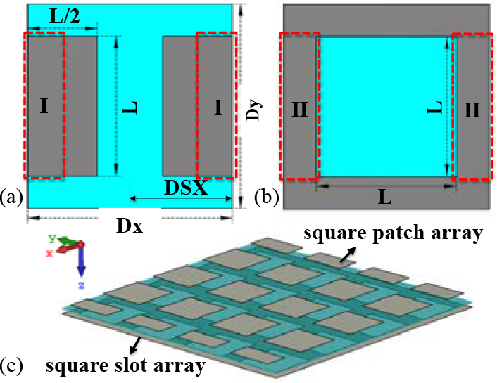
Figure 1: The unit cell of the proposed CFSS design. (a) The unit cell of square patch array. (b) The unit cell of square slot array. (c) The topology of the proposed CFSS (3-D view). The inset in (c) is the coordinated system.
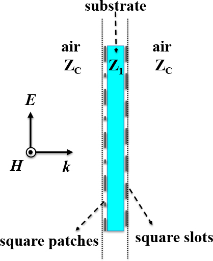
Figure 2: Side view of the proposed CFSS array.
B. Circuit analysis
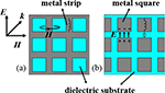
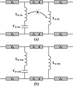
We define that TE-polarization is that the incident E-field is parallel to the y-axis and that of TM-polarization is parallel to the x-axis. Figure 3 shows the plane view of the proposed CFSS illuminated by the TE polarized plane wave. The metallic strip of square slot array that acts as an inductor for magnetic field is perpendicular to the wire as shown in Figure 3 (a). Capacitance formed between the adjacent edges of two coplanar square patches and inductance is associated with square patch. Thus, the square patch array interacts with E-field and behaves as a series LC circuit as shown in Figure 3 (b) [8]. The substrate between square patches and square slots can be considered as a short transmission line. Hence, the proposed CFSS is equivalent to a parallel combination of inductor and a series LC circuit, as shown in Figure 4, where Z is the intrinsic impedance of air and Z is the intrinsic impedance of the dielectric substrate. The thickness of the substrate d is relatively small, and its equivalent transmission line could be neglected in this work. The different transmission responses to TE- and TM-polarization incidence account for the electromagnetic coupling that occurs between square patches and square slots.
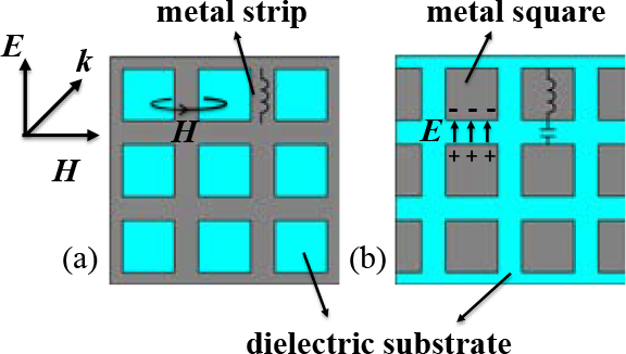
Figure 3: Plan view of the proposed CFSS array and their equivalent circuit. (a) The square slot array. (b) The square patch array.
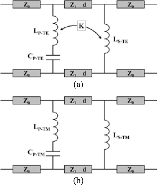
Figure 4: The equivalent circuit model of the proposed CFSS. (a) TE wave incidence. (b) TM wave incidence.
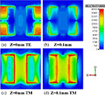
When a TE-polarized plane wave normally impinges on the composed CFSS structure, a strong coupling occurs around the metallic overlap area between I and II as shown in Figures 1 (a) and (b), which can be proved by the electric field distribution of square patch array and slot array at the resonance peaks shown in Figures 5 (a) and (b) where the E-field is concentrated on the overlap area.
The magnetic field induced by the current flowing on the square patch encircles the patch itself; hence, a portion of that field couples through the strips of the slot array because of overlap. Meanwhile, the current on the strips of square slot array produces a magnetic field that couples to the square patches. The mutual coupling between two layers is modeled as the mutual inductance as shown in Figure 4 (a) [9]. According to the transmission line and circuit theory, the CFSS sheet impedance Z can be found as follows:
| (1) |
Hence, the transmission zero frequency of the proposed CFSS in the TE-polarization case [10] is
| (2) |
where , , and M is the mutual inductance.
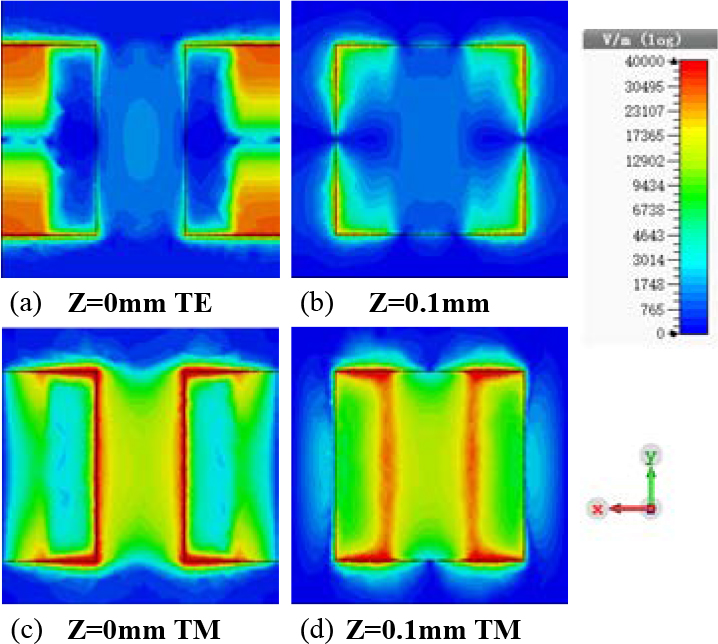
Figure 5: The electric field distribution of the proposed CFSS at 24.5 GHz. (a) TE mode, the electric field distribution of square patch array. (b) TE mode, the electric field distribution of square slot array. (c) TM mode, the electric field distribution of square patch array. (d) TM mode, the electric field distribution of square slot array.
When a TM-polarized plane wave normally incidents on the proposed CFSS, a weak coupling occurs between square patches and square slots. EM coupling between two layers can directly lead to the change of electromagnetic field distribution, which can be manifested by the electric field distribution at resonance shown in Figures 5 (c) and (d) where the E-field is concentrated on the gap between two square patches. The magnetic field induced by the current on the strips of square slot array is weak, and couples little to the patches, and vice versa. The coupling between the two complementary arrays would be ignored in this work as shown in Figure 4 (b). The CFSS sheet impedance Z can be found as follows:
| (3) |
Hence, the resonant frequency of the proposed CFSS in the TM-polarization case [10] is
| (4) |
All the parameters, such as DSX, D, L, as well as the thickness and permittivity of the dielectric substrate, determine the performance of the CFSS. Optimizing the structure and adjusting the coupling K make the transmission peak of TM-polarization equal to the transmission null of TE-polarization, that is,
| (5) |
where the CFSS shows polarization selective performance with a certain bandwidth.
The transmission coefficient of the proposed CFSS can be achieved by the following expression:
| (6) |
where is the impedance of the proposed CFSS structure.
A semi-analytic method is used to compute the values of the equivalent circuit parameters from the simulation. First, the transmission coefficient is obtained numerically by EM simulation, where commercial CST Microwave Studio is used in this work. Second, the least square method is applied to extract the equivalent lumped parameters of the equivalent circuit. Finally, the advanced design system (ADS) is used to test the extracted lumped parameters [11].
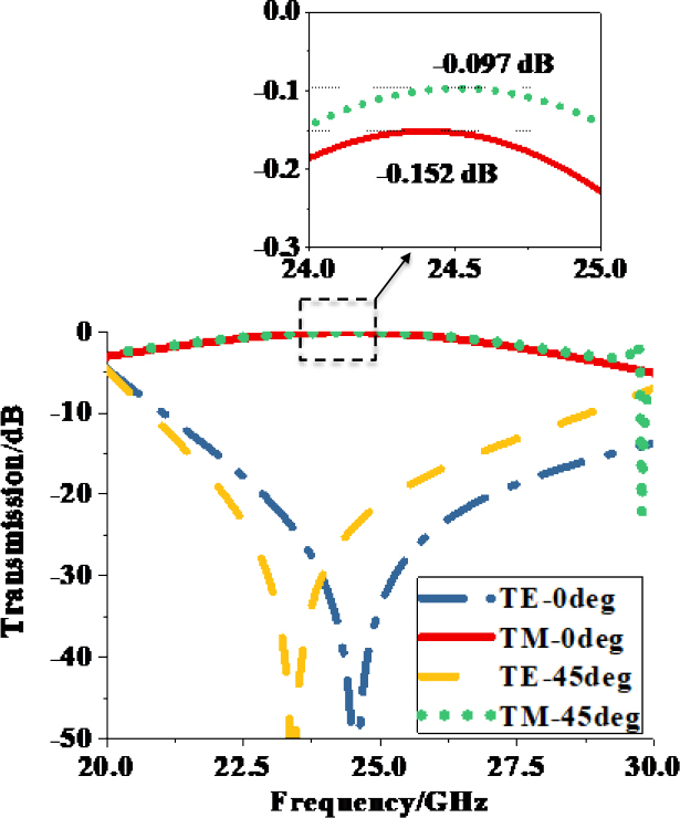
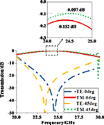
Figure 6: The transmission responses of the CFSS.
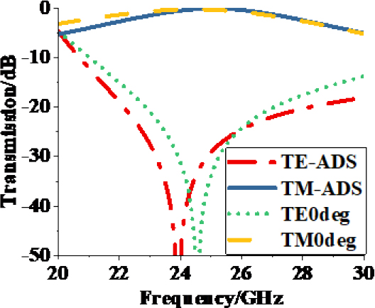
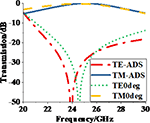
Figure 7: Transmission of the equivalent circuit and CFSS structure.
III. SIMULATION RESULTS
In order to verify our design, a full-wave analysis of the CFSS is performed using the commercial CST Microwave Studio. The parameters of an optimized CFSS design are D = 6 mm, L = 4.1 mm, and DSX = 3 mm. A thin dielectric substrate, with thickness of 0.1 mm and permittivity of 3, is sandwiched between the two complementary arrays. And its transmission responses of normal incidence and 45 incident angle for both polarizations are plotted in Figure 6. It is shown that the proposed CFSS has polarization selectivity and angular stability between 22.5 and 27.5 GHz.
The equivalent lumped parameters of the proposed CFSS are calculated with the semi-analytic method described in Section II-B. The extracted parameters are L= 212.64 pH, L= 318.5 pH, C= 0.3778 pF, K = 0.67, L= 101.68 pH, L= 410.18 pH, and C= 0.0786 pF. The results of the equivalent circuit using ADS and EM simulation results using CST are plotted in Figure 7, in which the simulated results are in good agreement.
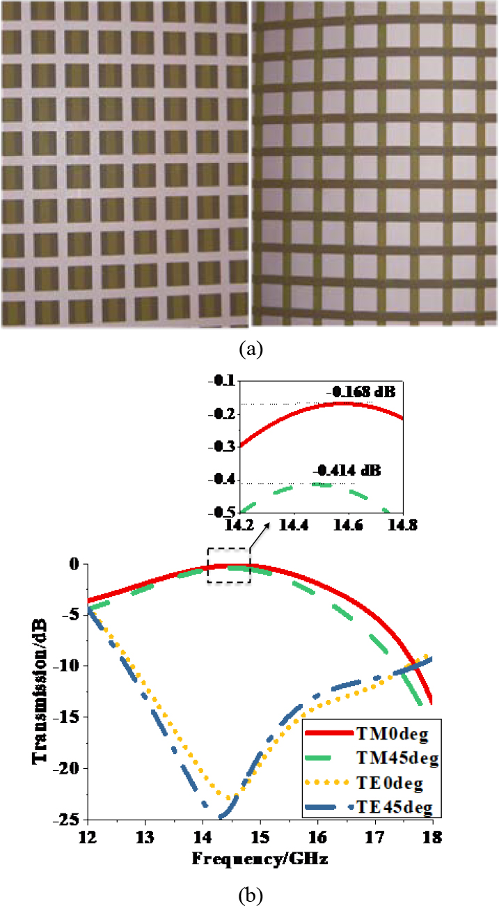
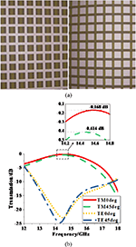
Figure 8: (a) The CFSS prototype. (b) Its measured transmission responses.
IV. EXPERIMENTAL VERIFICATION
A prototype was fabricated and its transmission responses were measured to validate the polarization selective performance. The parameters of the prototypes were re-optimized as L = 7.1875 mm and Dx = Dy = 10 mm under the limitation that the measuring range available to us is 12-18 GHz. Each array was printed on a thin polyimide with a thickness of 0.0254 mm, a dielectric constant of 3, and a loss tangent of 0.005. They were aligned and combined by a layer of EVA glue with a thickness of 0.045 mm, a dielectric constant of 3, and a loss tangent of 0.005. An Agilent N5224A vector analyzer and two horn antennas were used to measure the 400 mm 400 mm CFSS prototype shown in Figure 8 (a). The left is the square slot array and the right is the square patch array. The measured transmission responses of normal incidence and an oblique incidence angle of 45 are plotted in Figure 8 (b). It indicates that the proposed CFSS has polarization selectivity and angular stability.
V. CONCLUSION
In this paper, we propose a new CFSS structure with polarization selectivity and angular stability. The structure is based on the idea of using electromagnetic coupling to make the transmission peak of one polarization wave coincide with the transmission null of the orthogonal polarization wave. The circuit analysis is used to explain its filtering mechanism. A prototype of the proposed CFSS has been fabricated and its performance has been verified through experiment. It could be applied in various polarizer applications.
ACKNOWLEDGMENT
The authors would like to acknowledge the support by the Natural Science Foundation of Changchun Normal University (Grant No. 004[2019]) and Changchun Normal University Doctoral Research Fund (Grant No. 001[2020]BS).
REFERENCES
[1] M. S. Samani, R. S. Shirazi, and G. Moradi, “Multi-band frequency selective surface design based on idea of clusters in cellular communication systems,” Applied Computational Electromagnetic Society (ACES) Journal, vol. 30, no. 10, pp. 1079-1082, Oct. 2015.
[2] S. H. Wen and H. Y. Chen. “Design of a Jerusalem-cross slot antenna for wireless internet applications,” Applied Computational Electromagnetic Society (ACES) Journal, vol. 33, no. 1, pp. 15-22, Jan. 2018.
[3] L. W. Guo, S. M. Li, X. Jiang, X. Liao, and L. Peng, “Ultra-wideband transmissive linear polarization device based on graphene,” Applied Computational Electromagnetic Society (ACES) Journal, vol. 36, no. 7, pp. 914-921, Oct. 2021.
[4] B. Lin, W. Huang, L. Lv, J. Guo, Z. Wang, and R. Zhu, “Second-order polarization rotating frequency-selective surface,” IEEE Transactions on Antennas and Propagation, vol. 69, no. 11, pp. 7976-7981, Nov. 2021.
[5] M. Joyal and J. Laurin, “A cascaded circular-polarization-selective surface at K band,” 2011 IEEE International Symposium on Antennas and Propagation (APSURSI), Spokane, WA, pp. 2657-2660, Jul. 2011.
[6] X. Wu, Z. B. Pei, S. B. Qu, Z. Xu, P. Bai, J. F. Wang, X. H. Wang, and H. Zhou, “Design of metamaterial frequency selective surface with polarization selectivity,” Acta Phys. Sin., vol. 60, no. 11, pp. 279-283, Nov. 2011.
[7] J. Jiao, N. X. Xu, X. G. Feng, F. C. Liang, J. L. Zhao, and J. S. Gao, “Design and study of the active frequency selective surface based on the complementary screen,” Acta Phys. Sin., vol. 62, no. 16, pp. 364-369, Jul. 2013.
[8] K. Sarabandi and N. Behdad, “A frequency selective surface with miniaturized elements,” IEEE Trans. Antennas Propag., vol. 55, no. 5, pp. 1239-1245, May 2007.
[9] F. Bayatpur and K. Sarabandi, “Multipole spatial filters using metamaterial-base miniaturized-element frequency selective surfaces,” IEEE Trans. Microw. Theory Tech., vol. 56, no. 12, pp. 2742-2747, Nov. 2008.
[10] M. Moallem and K. Sarabandi, “Miniaturized element frequency selective surfaces for millimeter-wave to terahertz applications,” IEEE Trans. Terahertz Science Tech., vol. 2, no. 3, pp. 333-339, May 2012.
[11] H. A. Atallah, M. Alzubi, R. Hussein, and A. B. Abdlerhman, “Design of dual frequency coupled resonators using DGS and microstrip resonators for dual band WPT applications,” Applied Computational Electromagnetic Society (ACES) Journal, vol. 36, no. 1, pp. 75-81, Jan. 2021.
BIOGRAPHIES

Jian Jiao received the Ph.D. degree in optics from the Changchun Institute of Optics, Fine Mechanics and Physics, Chinese Academy of Sciences, China, in 2015.
She joined the School of Physics, Changchun Normal University, China, in 2019. Her research interests include frequency selective surface, and artificial electromagnetic material.

Nianxi Xub received the Ph.D. degree in optics from the Changchun Institute of Optics, Fine Mechanics and Physics, Chinese Academy of Sciences, China, in 2012.
He joined Key Laboratory of Optical System Advanced Manufacturing Technology Changchun Institute of Optics, Fine Mechanics and Physics, Chinese Academy of Sciences, China, in 2012. His research interests include frequency selective surface and functional thin films.

Jinsong Gao received the Ph.D. degree in optics from the Changchun Institute of Optics, Fine Mechanics and Physics, Chinese Academy of Sciences, China, in 2005. He was the Director of Key Laboratory of Optical System Advanced Manufacturing Technology Changchun
Institute of Optics, Fine Mechanics and Physics, Chinese Academy of Sciences, China, from 2008 to 2017. He has been the Director of Jilin Provincial Key Laboratory of Advanced Optoelectronic Equipment and Instruments Manufacturing Technologies since 2017. His research interests include optical thin films, frequency selective surface, and functional thin films.
ACES JOURNAL, Vol. 37, No. 4, 382–387.
doi: 10.13052/2022.ACES.J.370402
© 2021 River Publishers