Field Distribution Analysis Based on Improved Differential Algorithm for Dual Port Radiation Device
Shiqi Wang, Shaojun Fang, and Peng Chen
Department of Information Science and Technology
Dalian Maritime University, Dalian, Liaoning 116026, China
1609900643@qq.com, fangshj@dlmu.edu.cn, chenpeng213@126.com
Submitted On: August 8, 2021; Accepted On: March 8, 2022
Abstract
With the continuous development of science and technology, the requirement of signal source is higher and higher. Single port signal source is difficult to meet experimental requirements of radiation spatial field distribution. In this paper, a dual port radiation device for changing the field distribution is proposed. The dual port radiation device is mainly composed of the DC to 6 GHz experimental radiation device, amplifier, attenuator, and the phase shifter. After adding two different excitation signals to the dual port, the field distribution of the radiation device is calculated by improved differential algorithm and simulated by CST software. The simulated results are in good agreement with the calculated results. The innovation of this research lies in the dual port and controlling the field distribution of the radiation space freely.
Keywords: Field distribution, dual port, signal source, differential algorithm.
I. INTRODUCTION
With the increasing use of electronic chips and devices, electromagnetic radiation effect and its protection have become the focus of attention [1]. Signal source plays an important role in the detection and experiment of communications as well as in the biological field of studying the effect of electromagnetic radiation on cells. Field distribution is a highly important factor to ensure the validity of test results for electromagnetic field facilities [1]. Field uniformity is also addressed and required in some standards and works [2–4]. At present, there are many kinds of signal sources designed by existing technology, but there are still some problems, such as small frequency range adjustment, high noise, power and phase adjustment, and so on. Most of them are single port signal transmission rather than dual port signal sources, which are not suitable for analyzing the internal field distribution and controlling the field pattern. Most existing sources can provide a frequency range of 30 MHz to 3 GHz and higher frequency [5–7]. In [6], a radio frequency (RF) signal source with 40–160 MHz output frequency range is designed based on direct digital frequency synthesizer (DDS). In [7], a 143.4–151.5 GHz high DC-RF efficiency signal source in CMOS is introduced. In [8], a measurement of reflection coefficient of an 8.2–12.4 GHz RF signal source is introduced. In [9], a 0.01–70 GHz ultra-wideband and high output power signal source module is applied to RF and microwave test instruments. Some studies have shown that multi-port can provide better performance and meet requirements than single port [9–11]. In [10], a dual control and dual output current source from 0 to 12 A is designed for semi-conductor laser diode to meet the high power and high stability requirements. In [11], a dual-port intermodulation generator is introduced, which can be worked at 710 and 2550 MHz. In [12], a four-port high-frequency system for a 0.14-THz dual-sheet-beam hole-grating backward-wave oscillator is presented. The published paper [13] proposed a cylindrical coaxial radiation device with single port excitation in a small size. And the field distribution is not uniform in the frequency range. In recent years, based on the research of DC to 6 GHz broadband electromagnetic radiation experimental device, the field distribution in the radiation device is studied.
Because the field distribution in the single port radiation device is not very uniform, and it is not easy to control the internal field distribution, in order to solve the above technical problems and better control the distribution and uniformity of the electromagnetic field in the DC to 6 GHz radiation device, a dual port radiation device is proposed in the article. The proposed dual port radiation device is mainly composed of the DC to 6 GHz broadband experimental radiation device, amplifier, attenuator, and the phase shifter. The dual port radiation device uses the DC to 6 GHz experimental radiation device as the carrier of electromagnetic wave. By adding two signals with different amplitude and phase to the dual port radiation device, electromagnetic fields with different power and phase can be generated in the radiation space. In this way, the electromagnetic field in the radiation space can be freely controlled and changed to provide uniform electromagnetic field with good broadband characteristics. We use the CST Microwave Studio software to make the simulation [12–21]. Due to the large number of frequency points to be simulated, the simulation time of CST software is longer, and the memory space occupied is larger, which is not conducive to the research. Therefore, we propose an improved differential algorithm to calculate it, which saves simulation time and reduces memory space. Details of the analysis of field distribution are given and the related key parameters arediscussed.
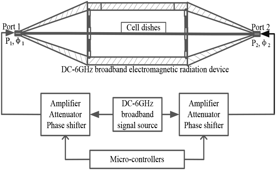
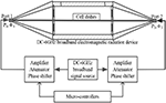
Figure 1: Structure of a dual port radiation device.
II. PRINCIPLES OF THE PROPOSED DEVICE
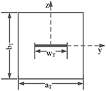
The configuration of the proposed dual port radiation device is shown in Figure 1. It consists of a DC to 6 GHz broadband electromagnetic radiation device, a broadband signal source, two adjustable amplifier modules, attenuators, and phase shifters. They are all controlled by a micro-controller and powered by a power supply module. It can be seen in Figure 1 that the broadband signal source generates two signals and passes through the amplifiers, attenuators, and phase shifters into signals with different power and phase . The cell dish is 35 mm in diameter and 10 mm in height and it is used to place cells. The cell dishes are placed in the inner conductor of the electromagnetic radiation device. These two different signals are added to the dual port of the radiation device respectively. Sinusoidal source signal is used for single port excitation. We can control the output frequency of the signal source according to the input data and input the data into the micro-controllers through the keyboard. And we can control the gain of dual port adjustable gain amplifiers, such as A-way and B-way and the last dual port output of the phase shifter, respectively. There is a wave detection device that can feedback the field strength of the experimental space. The integrated phase locked loop module has the advantage of low noise characteristics and saving development time. The amplifier module uses chip-compatible variable attenuator to achieve its gain control, while the micro-controllers will connect the keyboard and screen to input the required frequency and the power. In this way, we can change the power and phase of the signal source. By adding it to the two ports of the radiation device, two broadband signals with different power and phase can be generated to change the distribution of internal electromagnetic field.
III. DIFFERENTIAL ALGORITHM ANALYSIS AND SIMULATION
A. Differential algorithm analysis
The electromagnetic field values of each discrete point in the device are different, and the degree of variation is also different [12]. The field distribution of the TEM mode is solved by the two-dimensional Laplace equations, as shown in the following equation:
| (1) |
where is the scalar potential and is the Laplacian operator.
Given the initial value of each point, the electromagnetic field formula is analyzed and discretized, and the distribution of electric field is obtained in the following equations:
| (2) |
| (3) |
where is the electric field in the x direction, is the electric field in the y direction, and is the grid size.
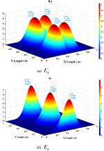
Differential algorithm is used to calculate the electromagnetic field distribution. In the calculation process, the phase and power (amplitude) are introduced by setting the initial amplitude and phase of the input signal. And the phase and power are further calculated by iteration. The frequency set in program calculation is 6 GHz. The 3-D field distribution of single port signal source by differential algorithm is shown in Figure 2. Figure 2 (a) shows the field distribution and Figure 2 (b) shows the field distribution, where a is half of the cross-sectional length of outer conductor plate and b is half of the cross-sectional length of outer conductor plate. x is the position coordinate in the length direction of the cavity and y is the position coordinate in the height direction of the cavity. As can be seen from Figure 2 (a), the peak value of field strength appears at x = 0.4a y = 0.776b, x = 0.6a y = 0.782b, x = 0.6a y = 0.28b, and x = 0.4a y = 0.274b. As can be seen from Figure 2 (b), the peak value of field strength appears at x = 0.5a y = 0.992b, x = 0.5a y = 0.504b, and x = 0.5a y = 0.006b.
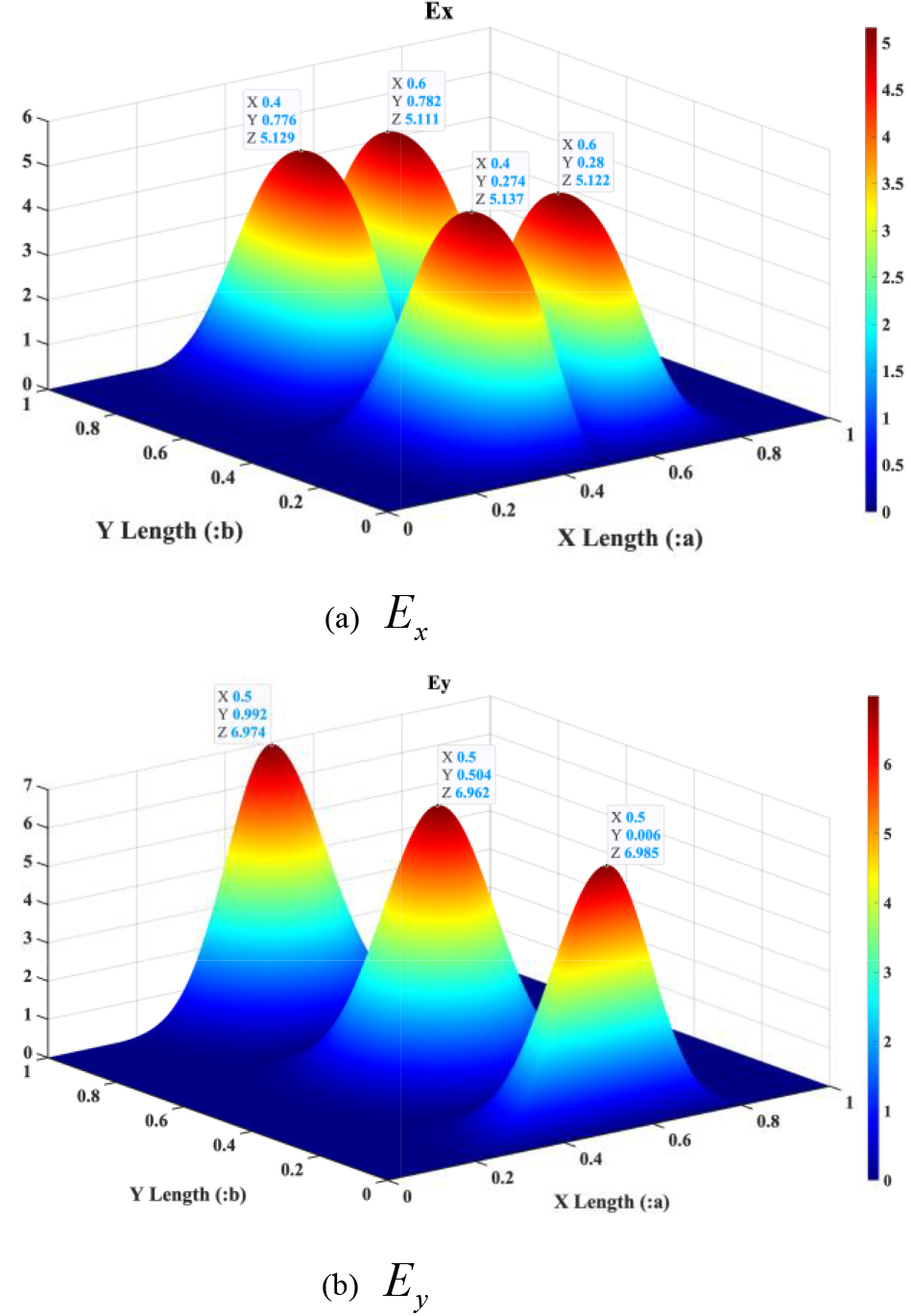
Figure 2: 3-D field distribution of single port signal source by differential algorithm.
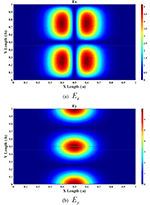
Field distribution of single port signal source in X-Y view by differential algorithm is shown in Figure 3. Figure 3 (a) shows the field distribution and Figure 3 (b) shows the field distribution. Figure 3 is the top view of Figure 2, respectively.
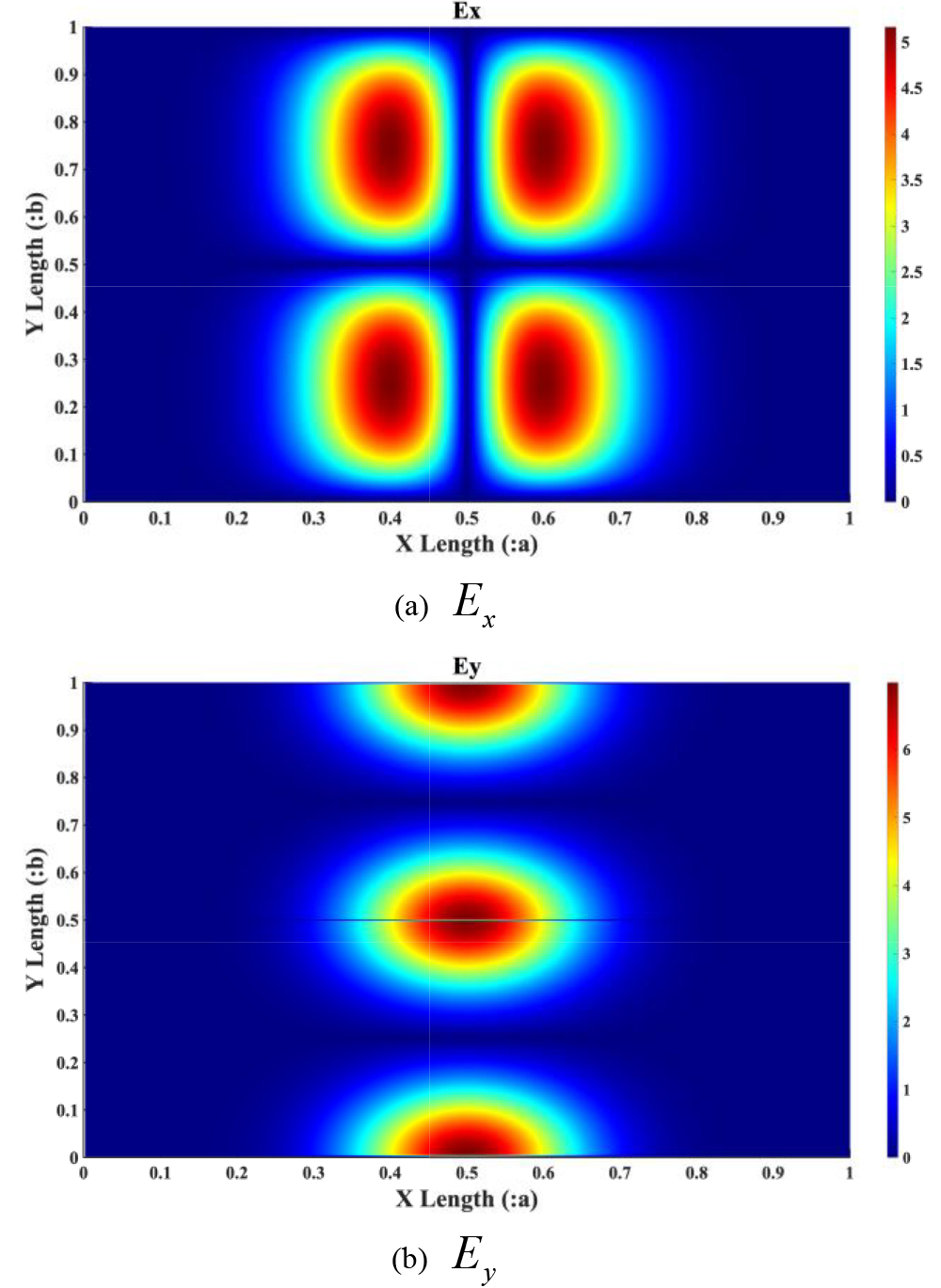
Figure 3: Field distribution of single port signal source in X-Y view by differential algorithm.
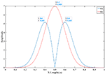
In order to observe the electric field distribution better, the field distribution of single port in one-dimension is shown in Figure 4. In Figure 4, the red dotted line shows the field distribution and blue line shows the field distribution of single port signal source in one-dimension. As can be seen from Figure 4, the peak value of field strength appears at x = 0.5a, and the amplitude is 7. The peak value of field strength appears at x = 0.4a and x = 0.6a, and the amplitude is 5.
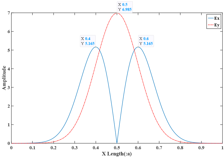
Figure 4: Field distribution of single port signal source in one-dimension.
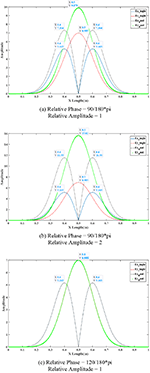
Figure 5 shows the field distribution of dual port in one-dimension. In Figure 5, the red dotted line shows the field distribution and blue line shows the field distribution of single port, the green line shows the field distribution, and black dotted line shows the field distribution of dual port. When the relative phase and amplitude of the dual port are changed, the field distribution and field distribution will also change. Because the field along the y direction is nearly unchanged, and the field along the x direction changes greatly in the placement area of the radiation device, we focus on the field along the x direction.
When the amplitude is constant, the relative phase is changed and some parameters are selected, the field distribution in one-dimension is shown in Figure 5 (a), (c), (e), and (g). Figure 5 (a) illustrates that the relative phase is 90/180*pi and the relative amplitude is 1. Figure 5 (c) illustrates that the relative phase is 120/180*pi and the relative amplitude is 1. Figure 5 (e) illustrates that the relative phase is 210/180*pi and the relative amplitude is 1. And Figure 5 (g) illustrates that the relative phase is 360/180*pi and the relative amplitude is 1. When the amplitude is constant, the relative phase changes from 90/180*pi, 120/180*pi to 210/180*pi, the amplitude of field and field decrease by nearly half. While the relative phase changes from 210/180*pi to 360/180*pi, the amplitude of field and field is nearly doubled. It can be seen from the above three figures that when the relative phase changes, the amplitude of the field distribution changes periodically. The maximum amplitude is twice that of the single port.
When the phase remains constant, we change the relative amplitude and some parameters are selected, the field distribution in one-dimension is shown in Figure 5 (b), (d), (f), and (h). Figure 5 (b) illustrates that the relative phase is 90/180*pi and the relative amplitude is 2. Figure 5 (d) illustrates that the relative phase is 120/180*pi and the relative amplitude is 2. Figure 5 (f) illustrates that the relative phase is 210/180*pi and the relative amplitude is 2. And Figure 5 (h) illustrates that the relative phase is 360/180*pi and the relative amplitude is 2. Comparing Figure 5 (b), (d), (f), and (g) with (a), (c), (e), and (h), respectively, when the relative amplitude changes, the amplitude of field distribution causes corresponding changes, the relative amplitude has changed to two times the original one. And when the relative amplitude becomes twice, the amplitudes of field and field increase.
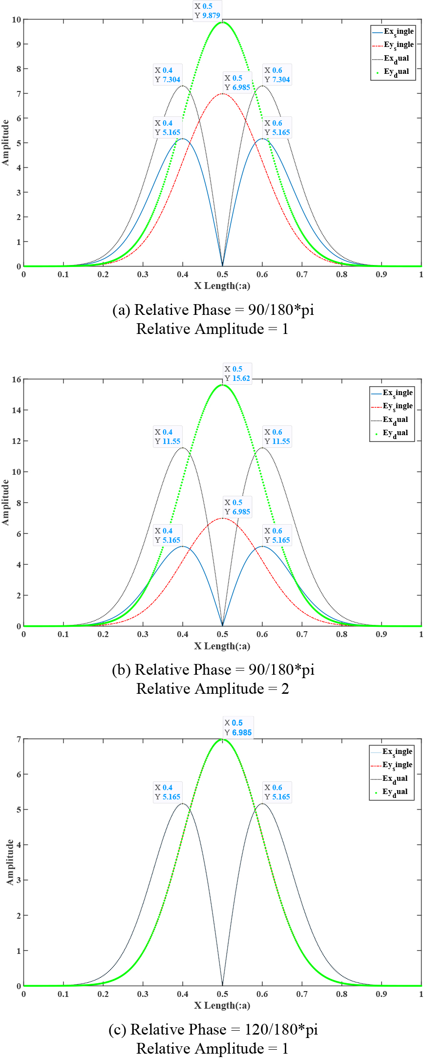
Figure 5: Field distribution of dual port signal source in one-dimension when relative phase and amplitude change.
B. CST simulation
The commercial software CST Microwave Studio Suite TM 2013 could be used to simulate the inner field distribution of the device [22–26]. The meshing parameters of CST simulation are provided in Table 1 and the boundary conditions are PEC boundary.
Table 1: Meshing parameters of the structure
| Meshing parameters | Values (mm) |
|---|---|
| Lower mesh limit | 5 |
| Min. mesh step | 0.154755 |
| Max. mesh step | 0.505055 |
| Meshcells | 4,670,784 |
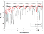
Figure 6 illustrates the cross-sectional structure of the DC to 6 GHz wideband electromagnetic radiation device, and Table 2 lists the structural parameters in the CST simulation process. The dimensions are as follows: a = 20 cm, b = 20 cm, w = 13.12 cm, L0 = 40 cm, and L1 = 36.5 cm, where a is the cross-sectional length of outer conductor plate, b is the cross-sectional length of outer conductor plate, w is the cross-sectional width of inner conductor plate, L0 is the length of intermediate cavity of the device, and L1 is the length of conical cavity on the side. Moreover, the device has to be symmetrical and its characteristic impedance is chosen to be . The characteristic impedance of 50 is provided by adjusting the ratio of the inner conductor to the outer conductor of the coaxial at the port. The reflection coefficient S is depicted in Figure 8. It depicts that the S is better than dB in the frequency range of DC to 6 GHz.

Figure 6: Cross-sectional structure of the device.
Table 2: Simulation parameters of the structure
| Structural parameters | a | b | w | L0 | L1 |
|---|---|---|---|---|---|
| Values (cm) | 20 | 20 | 13.12 | 40 | 36.5 |
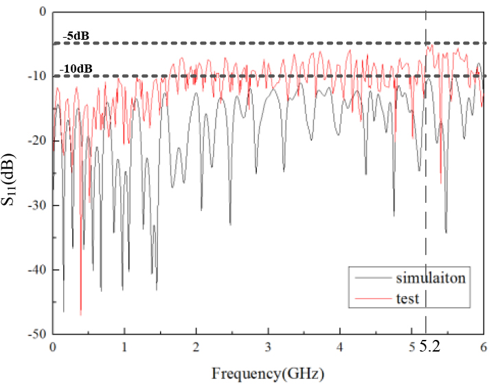
Figure 7: Reflection coefficient of the device.
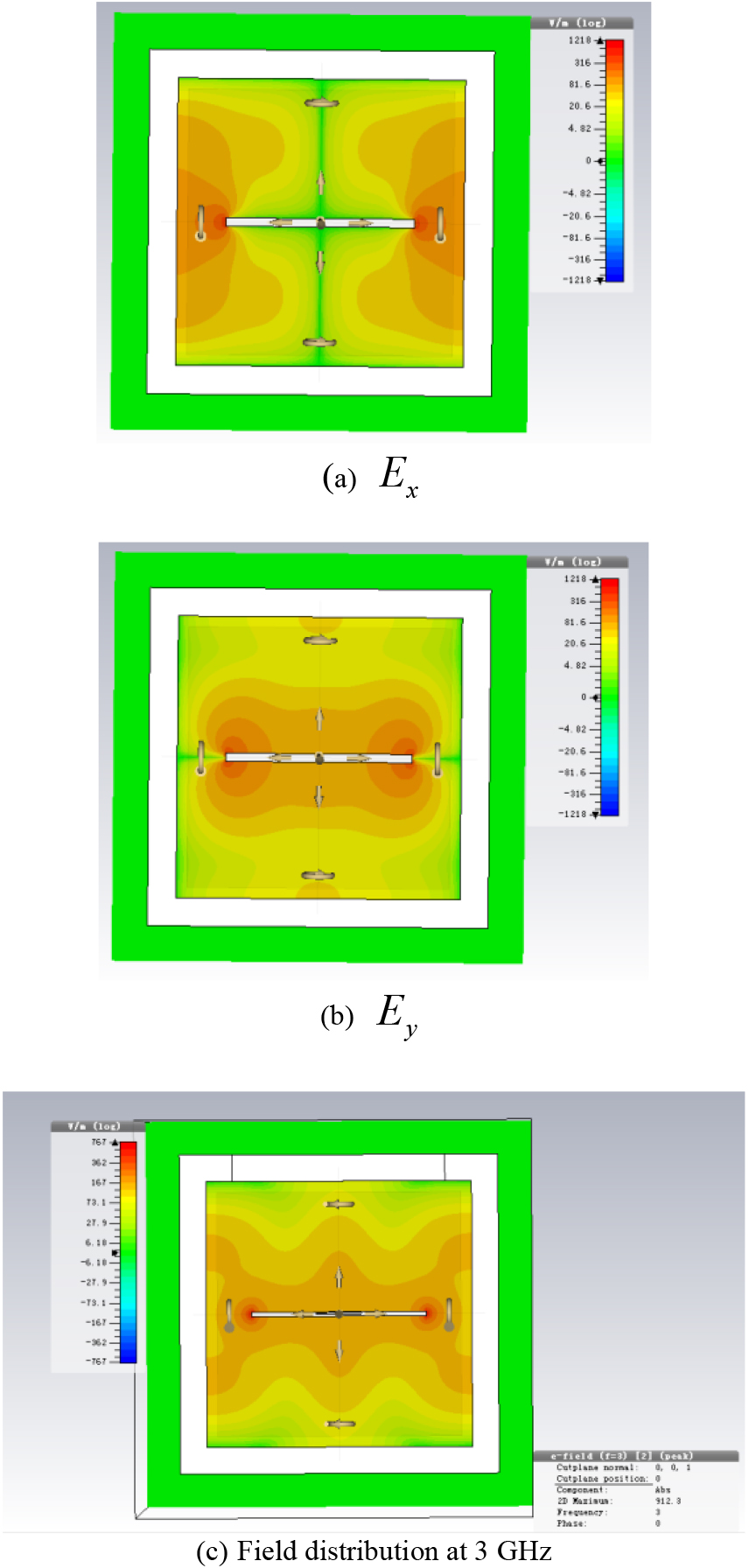
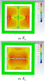
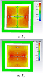
Figure 8: Field distribution of single port signal source.
When single port source was used in simulation, the other port was connected to the matching load. Field distribution of single port signal source is shown in Figure 8. Figure 8 (a) shows the field distribution and Figure 8 (b) shows the field distribution at 6 GHz. Figure 8 (c) shows that the electromagnetic field distribution at 3 GHz. It can be seen from Figures 3 and 8 that the peak values of appear on both sides, and the peak value of appears in the middle. Compared with Figure 3, the simulated results are basically consistent with the calculated results, which shows that the established model is correct. From this point of view, it is consistent in Figures 3 and 8. There are some deviations between the simulated results and the calculated results in some places, which are related to the thickness error of the dielectric plate at the edge of the intermediateconductor.
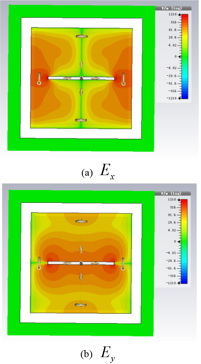
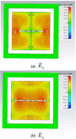
Figure 9: Field distribution of dual port signal source when .
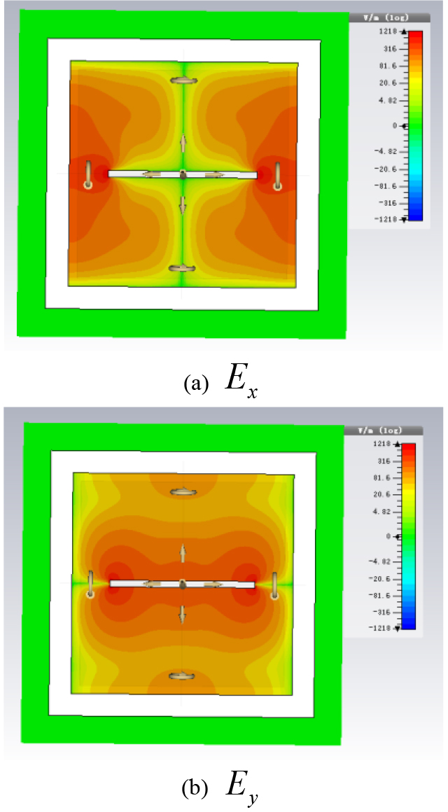
Figure 10: Field distribution of dual port signal source when .

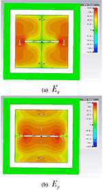
Figure 11: Field distribution of dual port signal source when .
When we add two different signal sources to ports of the device, the inner filed will be superimposed. Field distributions of dual port signal source are shown in Figures 9–12. Figures 9 and 11 illustrate the two different powers of the dual port signal source, which in Figure 8 and in Figure 11. Figure 9 (a) shows the field distribution and Figure 9 (b) shows the field distribution. Comparing Figure 8 with Figures 9 and 11, we can see that the strength of electromagnetic field has been superimposed on the radiation interface. Figure 11 illustrates the two different phases of the dual port signal source, which is . Figure 11 (a) shows the field distribution and Figure 11 (b) shows the field distribution. Comparing Figure 8 with Figure 11, we can see that the electromagnetic fields of the same phase are superimposed and offset at the radiation interface. Figure 12 illustrates the two different powers of the dual port signal source, which are and . As can be seen from Figure 12, when we change the power of each port, the strength of electromagnetic field will be superimposed on the radiation interface. And when we change the phase of each port, the electromagnetic field will be superimposed and offset by the same phase. It can be seen from the simulated results and calculated results that the trend and results are consistent, which shows that this method is feasible. In this way, we can change and control the electromagnetic field precisely.
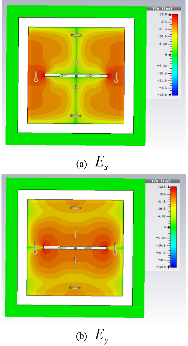
Figure 12: Field distribution of dual port signal source when and .
IV. COMPARISON OF THE SINGLE PORT DEVICE
Table 3 summarizes the performance comparison between the proposed dual port radiation device and previously reported designs for radiation experiments.
Table 3: Comparison between the proposed dual port radiation device and previously reported designs
| Ref. | Structure | Frequency range (GHz) | Field distribution |
|---|---|---|---|
| [11] | Dual-port intermodulation generator | 710–2550 MHz | |
| [12] | Four-port high-frequency system | 0.14 THz | |
| [14] | Twin TEM cells | 200 MHz | TEM |
| [16] | Twin TEM cells | 1 GHz | TEM |
| [17] | TEM/GTEM cell | ||
| [20] | Multi-step/piecewise linear TEM cell | DC to 1 | TEM |
| This work | Dual port device | DC to 6 | Uniform TEM/TM/TE |
The proposed dual port radiation device shows the widest frequency range compared with other designs [17, 20] for the radiation frequency range. In the item of field distribution, the proposed dual port device can control the field distribution and ensure the uniformity of the field in the radiation space compared with [14] and [16]. In general, the proposed dual port device has obvious advantages in the uniform field distribution and broadband aspect.
V. CONCLUSION
In this paper, a dual port radiation device is proposed, which can change the power and phase of the signal source. In this way, we can generate broadband signals with different power and phase to change the distribution of the electromagnetic field in the radiation space. Field distributions of the dual port radiation device for improved differential algorithm and CST simulation are provided. Its construction is given, and the related key parameters are discussed. Therefore, numerical and simulation analysis from DC to 6 GHz was carried out to define the usability of the system for well-controlled device. Based on the theoretical analysis and simulation calculations, the electromagnetic field distribution is generally shown. This characterization is assumed to be the fundamental prerequisite before considering the presence of cell dishes within the radiation device for radiation experiments of these new and widespread used telecommunication frequencies. Therefore, the proposed device can control the electromagnetic field in the radiation space. And the field distribution can be calculated with the proposed differentialalgorithm.
REFERENCES
[1] C. Baum, “Reminiscences of high-power electromagnetics,” IEEE Transactions on Electromagnetic Compatibility, vol. 49, no. 2, pp. 211-218, May 2007.
[2] L. Yao, J. Huang, N. Kang, T. Shen, D. Liu, F. Zhang, and H. Sun, “Implementation of a measurement system on field uniformity of transient electromagnetic field,” IEEE Electromagnetic Compatibility Magazine, vol. 5, no. 1, pp. 43-49, 2016.
[3] Electromagnetic Compatibility (EMC)-Part 4-3: Testing and Measurement Techniques- Radiated, Radio-Frequency, Electromagnetic Field Immunity Test, IEC 6l000-4-3: 2010, 2010.
[4] Electromagnetic Compatibility (EMC)-Part 4-20: Testing and Measurement Techniques- Emission and Immunity Testing in Transverse Electromagnetic (TEM) Waveguides, IEC61000- 4-20:2010, 2010.
[5] L. Yao, T. Shen, N. Kang, D. Liu, and J. Huang, “Time-domain simulation and measurement of a guided-wave EMP Simulator’s field uniformity,” IEEE Transactions on Electromagnetic Compatibility, vol. 55, no. 6, pp. 1187-1194,Dec. 2013.
[6] S. Chen, X. Han, and K. Chen, “The design of 40 160MHz RF signal source,” 2011 International Conference on Electric Information and Control Engineering, Wuhan, China, pp. 4598-4600, 2011.
[7] X. Meng, M. Zhou, B. Chi, and Z. Wang, “A 143.4-151.5 GHz high DC-RF efficiency signal source in 65nm CMOS,” 2019 IEEE International Conference on Integrated Circuits, Technologies and Applications (ICTA), Chengdu, China, pp. 1-2, 2019.
[8] K. Furuya and T. Inoue, “Measurement of reflection coefficient of RF signal source using a mismatch power meter with loss-less dielectric,” Conference Digest Conference on Precision Electromagnetic Measurements, Ottawa, Ontario, Canada, pp. 78-79, 2002.
[9] S. Zhang, G. Fan, Q. Li, and A. Zhao, “Design of a 0.01GHz–70 GHz high output power signal source module,” 2017 Progress in Electromagnetics Research Symposium - Fall (PIERS - FALL), Singapore, pp. 2241-2246, 2017.
[10] H. Xue, Y. Che, W. Teng, Y. Ma, and L. Ge, “Design of dual control and dual output constant current source for semi-conductor laser diode,” 2013 5th International Conference on Power Electronics Systems and Applications (PESA), Hong Kong, China, pp. 1-4, 2013.
[11] X. Chen, Y. He, and W. Cui, “Broadband Dual-Port Intermodulation Generator for Passive Intermodulation Measurements,” IEEE Microwave and Wireless Components Letters, vol. 27, no. 5, pp. 518-520, May, 2017.
[12] X. Tang, Z. Yang, K. Khan, N. Muhammad, and Z. Ouyang, “Theoretical and cold-test investigation of a four-port high-frequency system for a 0.14-THz dual-sheet-beam backward-wave oscillator,” IEEE Transactions on Electron Devices, vol. 65, no. 11, pp. 5068-5074, Nov. 2018.
[13] S. Wang, S. Fang, and P. Chen, “Design and research of DC-6GHz broadband electromagnetic radiation experimental device,” Journal of Electronics & Information Technology, vol. 41, no. 5, pp. 1092-1097, 2019.
[14] C. Zhang and J. Fu, “Research on field distribution of TEM mode in TEM cells,” Journal of Xi’ An Jiaotong University, vol. 30, no. 09, pp. 121-125, 1996.
[15] F. Dai, M. Wang, and D. Su, “A design of new twin TEM cells,” 2005 IEEE International Symposium on Microwave, Antenna, Propagation and EMC Technologies for Wireless Communications, Beijing, China, vol. 1, pp. 10-13, 2005.
[16] M. Wang, “Research of the uniformity of electromagnetic field based on FDTD method,” Journal of Guizhou University (Natural Science), vol. 30, no. 06, pp. 23-28, 2013.
[17] C. Song and X. Feng, “A new design and implementation of expanding testing space of a transverse electromagnetic cell,” 2016 IEEE International Conference on Microwave and Millimeter Wave Technology (ICMMT), Beijing, China, pp. 967-969, 2016.
[18] V. Chechetkin, A. Korotkov, E. Golubenko, E. Sychugov, and P. Smirnov, “Investigation of the characteristics of the TEM cell model,” 2019 Ural Symposium on Biomedical Engineering, Radioelectronics and Information Technology (USBEREIT), Yekaterinburg, Russia, pp. 439-441, 2019.
[19] H. Cui, Y. Hu, and L. Pang, “Calculation and verification of uniform electromagnetic field for cell culture,” Tianjin society of Biomedical Engineering, vol. 61, 2010.
[20] L. Yao, T. Shen, N. Kang, J. Huang, D. Liu, F. Zhang, and H. Sun, “Use of a reference point method to calibrate the field uniformity when testing with transient electromagnetic fields,” IEEE Transactions on Electromagnetic Compatibility, vol. 59, no. 2, pp. 352-359, 2017.
[21] M. Arezoomand, M. Meybodi, and N. Noori, “Design of a TEM cell using both multi-step and piecewise linear tapering,” 2016 8th International Symposium on Telecommunications (IST), Tehran, Iran, pp. 571-574, 2016.
[22] Z. Chen, Y. Deng, and D. Deng, “Research on field uniformity calibration method of GTEM cell,” Safety&EMC, vol. 3, pp. 42-44+77, 2013.
[23] W. Zhang and Y. Cao, “Research and simulation analysis on radio propagation model in electromagnetic environment simulation,” Chinese Journal of Radio Science, vol. 27, no. 3, pp. 538-542+550, 2012.
[24] W. Ju, Study on the critical frequency and the cause of higher order modes in the GTEM Cell [D]. Southeast University, 2016.
[25] G. Zhao, Q. Liu, and J. Wang, “Homogenization of microwave field in rectangular resonator,” Science & Technology Vision, vol. 18, pp. 24+44,2016.
[26] V. Sebera, A. Nasswettrová, and K. Nikl, “Finite element analysis of mode stirrer impact on electric field uniformity in a microwave applicator,” Drying Technology, vol. 30, no. 13, pp. 1388-1396,2012.
BIOGRAPHIES

Shiqi Wang was born in Shenyang, China. She received the B.Eng. and M.Eng. degrees in information and communication engineering from Dalian Maritime University, Liaoning, China, in 2014 and 2017, respectively. She is currently working toward the Ph.D. degree with the Dalian Maritime University.
Her current research interests include wideband electromagnetic field, bioelectromagnetics, and optimization method.

Shaojun Fang received the Ph.D. degree in communication and information systems from Dalian Maritime University (DLMU), Liaoning, China, in 2001.
Since 1982, he has been with DLMU, where he is currently the Head Professor with the School of Information Science and Technology. His recent research interests include passive RF components, patch antennas, and computational electromagnetics. He has authored or coauthored three books and over 100 journal and conference papers. He was a recipient of the Best Doctor’s Dissertation Award of Liaoning Province in 2002 and the Outstanding Teacher Award of the Ministry of Transport of China.

Peng Chen received the Ph.D. degree in communication and information systems from Dalian Maritime University (DLMU), Liaoning, China, in 2007.
He is currently an Associate Professor with the School of Information Science and Technology, DLMU. His current research interests include wireless sensor network, ultra-broadband wireless communication technology, and antenna.
ACES JOURNAL, Vol. 37, No. 4, 373–381.
doi: 10.13052/2022.ACES.J.370401
© 2021 River Publishers