Single-band Series Absorptive Common-mode Noise Filter
Ding-Bin Lin1, Erfansyah Ali1,2, Tjahjo Adiprabowo1, and Cheng-Yi Zhuang1
1Department of Electronic and Computer Engineering, National Taiwan University of Science and Technology, Taipei, Taiwan
dblin@mail.ntust.edu.tw, d10902801@mail.ntust.edu.tw, d10602804@mail.ntust.edu.tw, d10902010@mail.ntust.edu.tw
2Department of Telecommunication Engineering, Telkom University, Bandung, Indonesia
erfansyahali@telkomuniversity.ac.id
Submitted On: June 28, 2022; Accepted On: December 22, 2022
ABSTRACT
A Single-band Series Absorptive Common Mode Noise Filter (ACMF) is proposed. The ACMF is embedded in a four-layer printed circuit board (PCB) and consists of three parts: a Reflective Common Mode Noise Filter (RCMF), a matching circuit, and an absorber. The RCMF is designed using mushroom-type resonators. The matching circuit is designed using meander lines to reduce the size of the filter dimensions. The absorber of the Common Mode noise (CM) is a series resistor. The designed operating frequency is 2.45 GHz. The simulation results are as follows: the insertion loss of CM () is 22.49 dB at the frequency of 2.61 GHz, the return loss of CM () is 18.62 dB at the frequency of 2.5 GHz, while the integrity of the Differential Mode signals (DM) can be maintained with a very small insertion loss () of 1 dB at the frequency range of 0-8 GHz, and the achieved Absorption Efficiency (AE) is 93% at the frequency of 2.54 GHz. The proposed ACMF dimension is 10.3 x4.6 mm. The fractional bandwidth is 19%. The measurement results of the fabricated ACMF do not deviate significantly the simulation results. They are as follows: is 17.87 dB at the frequency of 2.31 GHz, Scc11 is 20.87 dB at the frequency of 2.38 GHz, is 2.8 dB at the frequency range of 0–8 GHz, the Absorption Efficiency is 97% at the frequency of 2.32 GHz, and the fractional bandwidth is 17%. Therefore, the results of the ACMF design carried out by simulation can be implemented into a fabricated ACMF with measurement results similar to the calculation results in the design.
Index Terms: absorptive common-mode filter (ACMF), absorption efficiency (AE), common-modefilter (CMF).
1 INTRODUCTION
Today, high-speed data transmission is used in many electronic systems, including Universal Serial Bus (USB) and High Definition Multimedia Interface (HDMI). The signals used are Differential Mode (DM) signals because of their high immunity to noise. However, some of these DM signals can turn into Common Mode (CM) signals as a result of the time skew and asymmetrical circuit structure. The CM signals will degrade the performance of electronic devices surrounding it, as they can cause the problem of radiated Electromagnetic Interference (EMI) noises [1, 2]. Therefore, the CM signals are considered as noise which is commonly referred to as CM noise [3–5]. To overcome this, a Common Mode noise Filter (CMF) is needed which is expected to reduce the CM noise at a certain frequency needed while maintaining the integrity of the DM signals.
In the past, many types of CMFs were proposed to overcome CM noise [6–8]. One of them is the use of a ferrite core with winding lines. This results in a large input impedance for CM noise [9], while the DM signals can still pass without significant attenuation. The disadvantage is that its bandwidth at high frequencies is limited due to decreased permeability. The next type of CMF proposed is the use of mushroom-like resonators in multilayer PCBs [10]. Next, RCMFs are made of Pattern Ground Structure (PGS). This structure provides a resonator in the reference ground plane to block the flow of CM noise [11]. The above-mentioned CMFs can prevent the transmission of CM noise to the next stage, because the CM noise is reflected to the front-end circuit by the filter. As a result, interference by CM noise is still sensed by the front-end and surrounding circuits. To overcome this problem, a filter type that can absorb CM noise energy is proposed.
There are two types of CMFs, namely: Reflective Common Mode Noise Filter (RCMF) and Absorptive Common Mode Noise Filter (ACMF). RCMF reflects CM noise to circuits in the previous stage. ACMF absorbs or dampens CM noise at certain frequencies so it does not continue to transmit to the next stages of the circuits and also does not bounce back to the previous stages of the circuits. The reflective CM noise will degrade the performance of the previous stages of the electronic circuits. Therefore, ACMF is better than RCMF. An ACMF can be made by adding absorber circuits in the form of resistive materials to an RCMF to absorb the reflected CM noise [12].
In this paper, a series ACMF is proposed. The ACMF consists of three stages. The first stage is the RCMF, the second stage is the matching circuit, and the third stage is the absorber in the form of a series resistive material. The RCMF type that is designed is a mushroom type. The matching circuit function is to bring a short circuit in the middle of the RCMF to the absorber which is located on the front port. Therefore the length of the matching circuit is half wavelength (/2) of the resonant frequency so that the short circuit condition reaches the absorber. The matching circuit is designed using meander lines to make the filter dimensions as small as possible. The absorber that is used is a Surface Mounted Device (SMD) resistor. The advantage of a series ACMF over another type of filter is its simpler implementation. The other type of ACMF filter is parallel ACMF. A series ACMF is implemented on a four-layer Printed Circuit Board (PCB).
An ACMF is said to be useful only if it is able to absorb as much CM noise as possible. This occurs when the insertion loss of CM () is minimum and the return loss of CM () is also minimum. This is expressed in terms of Absorption Efficiency (AE) as shown in (1) [13]. Therefore, the larger the AE the better the ACMF.
| (1) |
2 PROPOSED STRUCTURE
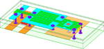
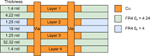
The structure of the proposed ACMF is shown in Fig. 1. This series ACMF uses four Layers PCB with detail dimensions and materials can be seen in Fig. 2. Layer 1 is used for differential mode signal traces. Layer 2 is used for the mushroom pad and reference ground of the matching circuit. While Layer 3 is used for local ground. Layer 4 is used for system ground and the location where the serial Surface Mounted Device (SMD) Resistor is attached.

Figure 1: The structure of proposed ACMF, trimetric view.
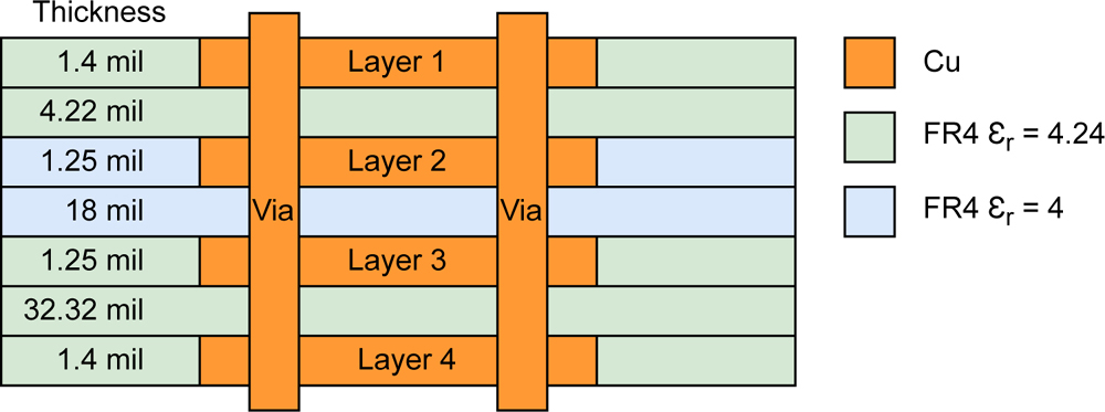
Figure 2: PCB layers of proposed ACMF.
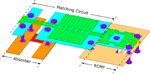
The series ACMF is shown in Fig. 3. The RCMF that we use in stage 1 is a mushroom-type RCMF. Therefore, the mushroom pad acts as an auxiliary ground for DM signals on stage 1. The mushroom pad is connected to the local ground at Layer 3 through a via and meandering path as shown in Fig. 1. This meandering path serves as an inductor that determines the resonant frequency. This is the frequency when transmission zero occurs for CM noise. The resonant frequency that we use is 2.45 GHz. This frequency was deliberately chosen according to the Wi-Fi frequency standard [14], so that our proposed ACMF can be used to secure the Wi-Fi transceiver module from the interference of CMnoise.
Transmission Zero or short circuit load occurs in the middle of the mushroom pad. The matching circuit in stage 2 has a function as a short circuit load shifter from the middle of the mushroom pad to the resistor absorber on stage 3. This is achieved by adjusting the length of the matching circuit to /2, where is the wavelength of the resonant frequency. To reduce the physical dimensions of the filter, this matching circuit is made in meander form. This results in the proposed ACMF dimensions of 10.3x4.6 mm. Thus, at stage 3, the CM noise will go through a short circuit and an absorbent resistor that is mounted serially towards the ground. This is a new concept of our research, which is to use an absorbent resistor in series rather than parallel. The advantage of this concept is its simplicity in implementation. The absorbent resistor is drawn in red as shown in Fig. 1 and Fig. 3. This is how the CM noise is dissipated into heat by an absorbent resistor that has a resistance of 25 .

Figure 3: The structure of proposed ACMF.
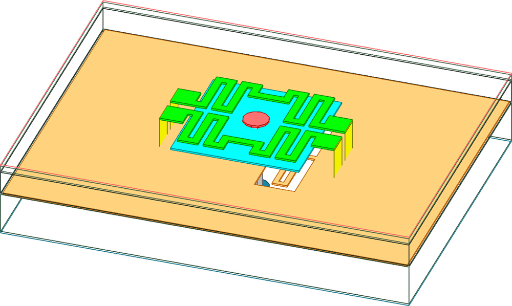
Figure 4: The structure of proposed RCMF.
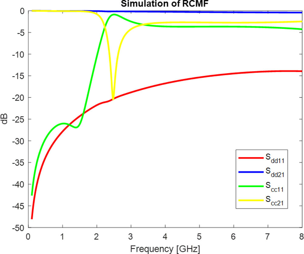
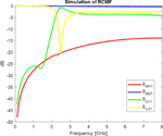
Figure 5: The simulation results of RCMF.
2.1 Reflective common mode noise filter (RCMF)
The first stage of our proposed ACMF is an RCMF. Its structure is shown in Fig. 4. It is a mushroom-type RCMF. Its working frequency is 2.45 GHz. The transmission zero of the mushroom-type RCMF happens in the middle of the structure. The simulation results of the mushroom type RCMF is shown in Fig. 5. The dimension of this RCMF is 3x2.5 mm.
It is seen in Fig. 5 that only decreased slightly (less than 1 dB) for the frequency range of 0–8 GHz. This shows that the integrity of the differential signals is well maintained. We also see that the insertion loss of CM reached its lowest value of around 20 dB at 2.45 GHz. Meanwhile, the return loss of CM reached its highest value (less than 1 dB) at a frequency of 2.45 GHz. This means that at a frequency of 2.45 GHz the common mode noise is not transmitted to the next device but is reflected back to the previous device. This proves that this filter is an RCMF.
2.2 Matching circuit
The function of the Matching Circuit is to bring the short circuit impedance from the center of the RCMF to the input port of the series-type absorber. The goal is that as much of the reflected common mode noise energy that occurs in the center of the RCMF is channeled to the absorber to be dissipated into heat so that it does not flow to the device located at the ACMF input. This matching circuit is implemented using a transmission line with a length of /2, where is the electromagnetic wavelength with a frequency of 2.45 GHz, which is the ACMF working frequency. To reduce the dimensions, the matching circuit transmission line is made in the form of ameander.
2.3 Series-type absorber
The absorber is used to absorb the CM noise energy reflected by the RCMF by passing it through a resistor so that the energy turns into heat. By dissipating the CM noise energy into heat, the CM noise energy no longer interferes with RF (Radio Frequency) devices around it. This absorber is implemented using a 0805 SMD resistor and is installed in serial position with the system ground through which common mode energy passes. Technically, we cut the system ground plane immediately after the input port of the ACMF so that there is a gap in the system ground. Into this gap an SMD resistor is serially installed in such a way that the SMD resistor connects the two planes of the cut off system ground. This SMD resistor is safe and suitable for use in ACMF because the maximum power that can be applied to this SMD resistor is 0.5 W and its size is 2.00×1.25×0.50 mm [13]. The resistance used for this SMD resistor is 25 . This absorber resistance is chosen according to the input impedance of the CM noise so that the transfer of CM noise energy to the absorber is maximum.
3 SIMULATED AND FABRICATED ACMF
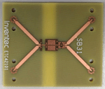
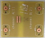
This section presents measurement results both in simulation and fabricated of designed ACMF. The simulation was made by using HFSS software from Ansys and the real ACMF was made at the factory based on this simulation. We named it the fabricated ACMF and it is shown in Fig. 6 and Fig. 7, which are the fabricated ACMF top view and bottom view, respectively.

Figure 6: Fabricated ACMF, top view.
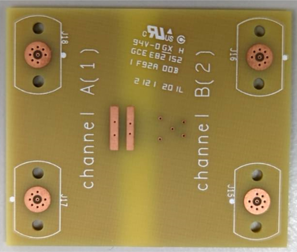
Figure 7: Fabricated ACMF, bottom view.
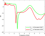
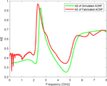
The measurement results of the simulated ACMF are shown in Figs. 8-11 in green line, meanwhile the measurement results of the fabricated ACMF are shown in red line. The comparison between them is shown in Table1.
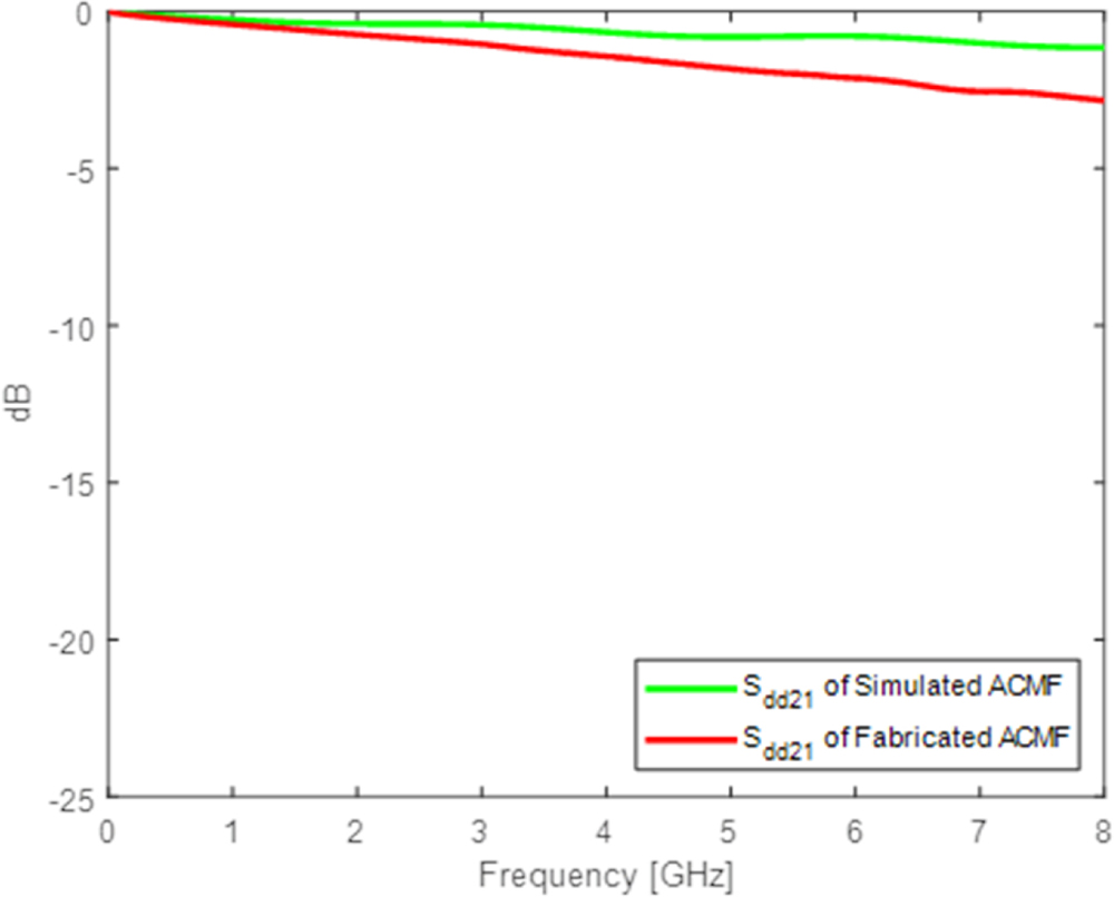
Figure 8: The comparison between the of the simulated and fabricated ACMF.
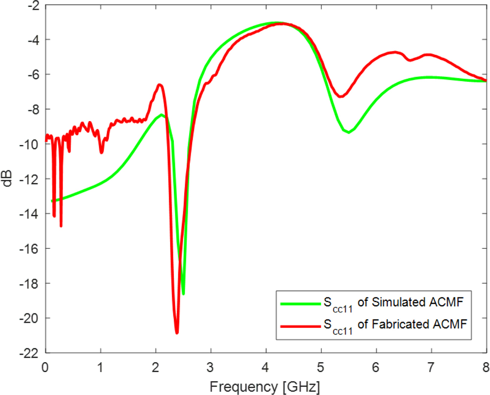
Figure 9: The comparison between the of the simulated and fabricated ACMF.
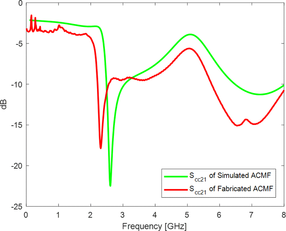
Figure 10: The comparison between the of the simulated and fabricated ACMF.
Table 1: Comparison between Simulation and Fabrication
| Simulation | Fabrication | |||
|---|---|---|---|---|
| 22.49 dB | 2.61 GHz | 17.87 dB | 2.31 GHz | |
| 18.62 dB | 2.5 GHz | 20.87 dB | 2.38 GHz | |
| 1 dB | 8 GHz | 2.8 dB | 8 GHz | |
| AE | 92.8% | 2.54 GHz | 97% | 2.32 GHz |
| Fract. BW | 19% | 17% | ||
Table 2: Comparison between Series and Parallel ACMF
| Parameter [Unit] | This Paper | Paper [18] | Paper [19] | Paper [20] |
| Absorption freq. [GHz] | 2.32 | 2.25 | 3.55 | 2.45 |
| Absorption efficiency [%] | 97 | 96 | 97 | 97 |
| Dimensions [mm] | 10.3 x4.6 | 8.65x2.5 | 28.6x13.5 | 16x3.5 |
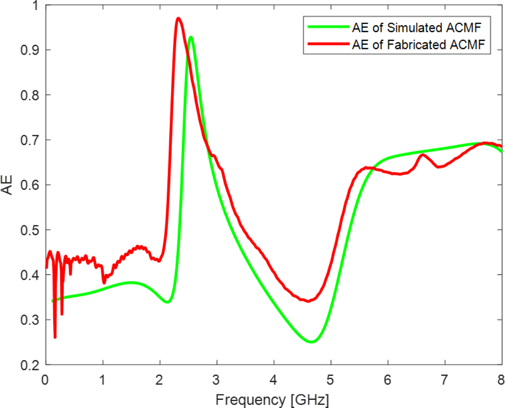
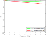
Figure 11: The comparison between the Absorption Efficiency of the simulated and fabricated ACMF.
4 DISCUSSIONS
S parameter is used to analyze the characteristics of common mode filters. The ones that are often used are , , and [6, 8,15–17]. is the insertion loss of DM which is ideally 0 dB. is the insertion loss of CM which is ideally dB. is the return loss of CM which is ideally dB for ACMF.
From simulation results, Fig. 8 shown that is 0.4 dB at frequency 2.45 GHz. Therefore, the insertion loss of DM signal in our simulation is very small, i.e. integrity of the DM signal that is passed in the proposed ACMF is well maintained. Figure 9 shown that for the frequency of 2.45 GHz is about 19 dB. his means that the reflected CM noise in our simulation has been reduced quite significantly. Figure 10 shown that the minimum for with a level of 23 dB occurs at a frequency slightly above 2.45 GHz. This means that the CM attenuation in our simulation is very large and occurs slightly above the expected frequency. In Figure 11, it can be seen that the maximum absorption efficiency of about 93% occurs at a frequency of around 2.5 GHz. As a result, at a frequency of around 2.5 GHz, our simulation succeeded in reducing and absorbing 93% of the CM noise that passes through it.
The real ACMF was fabricated at the factory based on this simulation as shown in Figs. 6 and 7. The comparison between the measurement results and the simulation results are shown in Figs. 8–11 in which we can clearly see that the S parameter measurements are slightly different from the measurement results in the simulation. These differences are caused by the addition of transmission lines, which are used to connect ACMF ports with measurement terminals as we can see in Fig. 6. However, these differences can be tolerated because they are small and the overall results of these measurements show the same pattern and close similarity.
In addition, the absorption efficiency obtained from fabricated ACMF is also greater than that obtained from simulated ACMF. This AE, which is generated by a series ACMF, is also compared with the AE generated by a parallel ACMF and made by other researchers [18] as shown by Table 2.
Table 2 is a comparison of the data between the ACMF that we made and several ACMFs produced by other researchers as written in the papers [18–20]. Frequency absorption occurs at adjacent frequencies, namely: 2.32 GHz, 2.25 GHz, 3.55 GHz, and 2.45 GHz, so this comparison is valid because the ACMF works at adjacent frequencies. Although our ACMF dimension is larger than the ACMF dimension reported by the paper [18], the Absorption efficiency generated by our ACMF is greater than the ACMF absorption efficiency reported by the paper [18]. Papers [19, 20] reported absorption efficiencies similar to absorption efficiency produced by our ACMF, but our ACMF dimension is smaller than those reported in the same papers.
In addition, the fabricated series ACMF can maintain the integrity of differential signal well. As we can see in Fig. 8, it can be seen that at a frequency of around 2.5 GHz the DM insertion loss value of is less than 1 dB. Thus, we can conclude that the simulation of the series ACMF that we have designed has been successful and can be implemented on the PCB with good S parameter measurement results.
5 CONCLUSIONS
The motivation of this research is to identify a technique to reduce CM noise at a frequency of 2.45 GHz so as not to interfere with RF devices operating in the vicinity of this frequency, such as Wi-Fi transceiver module. Our experiment solved this problem with the success of our simulated ACMF and fabricated ACMF to reduce CM noise at the frequency of near the 2.45 GHz. We use an SMD resistor in our ACMF to absorb CM noise. The absorption efficiency that we managed to achieve in the simulation was 93%, while our fabricated ACMF managed to achieve an absorption efficiency of 97%. In addition, our simulated ACMF and fabricated ACMF also managed to maintain the integrity of the DM signal that passes through it with a DM insertion loss of less than – 0.5 dB and less than 1 dB respectively at frequencies of around 2.45 GHz. The next thing, the dimension of our proposed ACMF is also small. For future development, the method used in our experiment can be further developed to achieve better characteristics and smaller dimensions.
ACKNOWLEDGMENT
This work was supported by Ministry of Science and Technology of Taiwan (Grant MOST 110-2221-E-011-052).
REFERENCES
[1] C. Y. Zhuang, T. Adiprabowo, D. B. Lin, Y. H. Chen, Y. H. Zheng, B. H. Tsai, and A. A. Pramudita, “A broadband common-mode filter by using dual band transmission zero,” 2021 Asia-Pacific International Symposium on Electromagnetic Compatibility (APEMC), pp. 1-3, 2021.
[2] Z. Zhu, W. Yan, Y. Wang, Y. Zhao, T. Zhang, and J. Huang, “Noise analysis method of radiated EMI based on non-linear principal component analysis,” Applied Computational Electromagnetics Society (ACES) Journal, vol. 35, no. 10, p. 1144–1152, 2020.
[3] Z. Chen and G. Katopis, “A comparison of performance potentials of single ended vs. differential signaling,” Electrical Performance of Electronic Packaging - 2004, pp. 185–188, 2004.
[4] D. G. Kam, H. Lee, J. Kim, and J. Kim, “A new twisted differential line structure on high-speed printed circuit boards to enhance immunity to crosstalk and external noise,” IEEE Microwave and Wireless Components Letters, vol. 13, no. 9, pp. 411–413, 2003.
[5] E. Bogatin, Signal and Power Integrity, Simplified, Prentice Hall, Upper Saddle. River, NJ 3rd edn., 2018.
[6] W. T. Liu, C. H. Tsai, T. W. Han, and T. L. Wu, “An embedded common-mode suppression filter for GHz differential signals using periodic defected ground plane,” IEEE Microwave and Wireless Components Letters, vol. 18, no. 4, pp. 248–250, 2008.
[7] F. de Paulis, L. Raimondo, S. Connor, B. Archambeault, and A. Orlandi, “Compact configuration for common mode filter design based on planar electromagnetic bandgap structures,” IEEE Transactions on Electromagnetic Compatibility, vol. 54, no. 3, pp. 646–654, 2012.
[8] S. J. Wu, C. H. Tsai, T. L. Wu, and T. Itoh, “A novel wideband common-mode suppression filter for gigahertz differential signals using coupled patterned gound structure,” IEEE Transactions on Microwave Theory and Techniques, vol. 57, no. 4, pp. 848–855, 2009.
[9] K. Yanagisawa, F. Zhang, T. Sato, K. Yamasawa, and Y. Miura, “A new wideband common-mode noise filter consisting of Mn-Zn ferrite core and copper/polyimide tape wound coil,” IEEE Transactions on Magnetics, vol. 41, no. 10, pp. 3571–3573, 2005.
[10] B. F. Su and T. G. Ma, “Miniaturized common-mode filter using coupled synthesized lines and mushroom resonators for high-speed differential signals,” IEEE Microwave and Wireless Components Letters, vol. 25, no. 2, pp. 112–114,2015.
[11] H. W. Liu, C. H. Cheng, P. J. Li, and T. L. Wu, “A novel compact single-stage absorption common-mode filter,” IEEE Transactions on Electromagnetic Compatibility, vol. 64, no. 1, pp. 111–118, 2022.
[12] H. W. Liu and T. L. Wu, “A wideband single-cell unidirectional absorption common-mode filter with pattern ground structure,” 2022 Asia-Pacific International Symposium on Electromagnetic Compatibility (APEMC), pp. 13–15, 2022.
[13] T. Adiprabowo, D. B. Lin, Y. H. Zheng, Y. H. Chen, C. Y. Zhuang, and B. H. Tsai, “Dual-band high absorbing and broadband suppressing common-mode noise filter,” IEEE Transactions on Electromagnetic Compatibility, pp. 1–10, 2021.
[14] “IEEE Standard for Information Technology — Telecommunications and information exchange between systems Local and metropolitan area networks—Specific requirements - Part 11: Wireless LAN Medium Access Control (MAC) and Physical Layer (PHY) Specifications,” IEEE Std 802.11-2016 (Revision of IEEE Std 802.11-2012), pp. 1–3534, 2016.
[15] C. H. Wu, C. H. Wang, and C. H. Chen, “Novel balanced coupled-line bandpass filters with common-mode noise suppression,” IEEE Transactions on Microwave Theory and Techniques, vol. 55, no. 2, pp. 287–295, 2007.
[16] C. H. Tsai and T. L. Wu, “Novel balanced coupled-line bandpass filters with common-mode noise suppression,” IEEE Transactions on Microwave Theory and Techniques, vol. 58, no. 1, pp. 195–202, 2010.
[17] X. H. Wu and Q. X. Chu, “Compact differential ultra-wideband bandpass filter with common-mode suppression,” IEEE Microwave and Wireless Components Letters, vol. 22, no. 9, pp. 456–458, 2012.
[18] P. J. Li, Y. C. Tseng, C. H. Cheng, and T. L. Wu, “A novel absorptive common-mode filter for cable radiation reduction,” IEEE Transactions on Components, Packaging and Manufacturing Technology, vol. 7, no. 4, pp. 511–518, 2017.
[19] S. K. Tseng, C. N. Chiu, Y. C. Tsao, and Y. P. Chiou, “A novel ultrawideband absorptive common-mode filter design using a miniaturized and resistive defected ground structure,” IEEE Transactions on Electromagnetic Compatibility, vol. 63, no. 1, pp. 66–73, 2021.
[20] P. J. Li, C. H. Cheng, and T. L. Wu, “A resistor-free absorptive common-mode filter using gap-coupled resonator,” IEEE Microwave and Wireless Components Letters, vol. 28, no. 10, pp. 885–887, 2018.
BIOGRAPHIES

Ding-Bing Lina (S’89–M’93–SM’14) received M.S. and Ph.D. degrees in Electrical Engineering from National Taiwan University, Taipei, Taiwan, in 1989 and 1993, respectively.
From August 1993 to July 2016, he was a Faculty Member with the Department of Electronic Engineering, National Taipei University of Technology (Taipei Tech), Taipei, Taiwan, where he was an Associate Professor, Professor, and Distinguished Professor in 1993, 2005, and 2014, respectively. Since August 2016, he has been a Professor with the Department of Electronic and Computer Engineering, National Taiwan University of Science and Technology (Taiwan Tech). He is currently directing a human resources cultivation program named the Promotion Center for 5G Antennas and Radio Frequency Techniques Consortium. He has authored or coauthored more than 200 papers in international journals and at international conferences, respectively. His research interests include wireless communication, radio multipath fading channel modeling, mobile antennas, high-speed digital transmission, and microwave engineering.
Dr. Lin was the recipient of the Annual Research Outstanding Award of the College of Electrical Engineering and Computer Science in 2004, 2006, and 2008. After he had received these three awards, the College of Electrical Engineering and Computer Science awarded him the College Research Outstanding Award to highlight his research achievements. He was also the recipient of the Taipei Tech Annual Outstanding Research Award in 2008. He was the Chair of the Taipei Chapter, IEEE Broadcasting Society, from 2010 to 2014, the Technical Program Committee Chair of the 2015 Asia-Pacific International EMC Symposium, and the Chair of the Taipei Chapter, IEEE EMC society from 2015 to 2018. He has been on the Associate Editor of the IEEE Transaction on EMC since 2019 and the Editorial Board of the International Journal of Antennas and Propagation since 2014.
Erfansyah Alia received B.Eng. (2005) and M.Eng. (2012) degrees in Communications from the Electrical Engineering Department, Intitut Teknologi Bandung (ITB). Currently, he is a lecturer at School of Electrical Engineering, Telkom University, and a PhD student at National Taiwan University of Science and Technology (NTUST). His research interests are in Radar Systems, RF device, and Signal Processing.

Tjahjo Adiprabowoa received a B. Eng. degree in Telecommunication Engineering from Bandung Institute of Technology, Bandung, Indonesia, in 1987, and a M. Eng. degree in Telecommunication Engineering from Royal Melbourne Institute of Technology, Melbourne, Australia, in 2001. He is now pursuing a Ph.D. degree in Wireless Engineering at the Department of Electronic and Computer Engineering in National Taiwan University of Science and Technology, Taipei, Taiwan. From 1987 to 1991, he worked as a Satellite Ground Station Engineer for PT. Elektrindo Nusantara, in Jakarta, Indonesia. From 1991 to 2000, he worked as a Mainframe System Programmer for PT. Telekomunikasi Indonesia, in Bandung, Indonesia. From 2001 to 2012, he worked as a Network Performance Engineer for PT. Telekomunikasi Indonesia, in Bandung, Indonesia. Since 2012, he has been a Lecturer in School of Electrical Engineering in Telkom University, in Bandung, Indonesia. His research interests include Wireless Engineering, Wireless Sensor Networks, Radar Engineering, and Common-Mode Noise Filters.

Cheng-Yi Zhuanga (S’20) was born in Pingtung, Taiwan. He received a B.S. degree in Electronic and Computer Engineering from National Taiwan University of Science and Technology, Taipei, Taiwan, in 2019, where he is currently pursuing a Ph.D. degree.
ACES JOURNAL, Vol. 37, No. 11, 1139–1145
doi: 10.13052/2022.ACES.J.371104
© 2022 River Publishers