On the Coupling Imbalance of the UWB BLC in the 5G Low Noise Amplifier Design
Tamer G. Abouelnaga1,2 and Esmat A. Abdallah1
1Microstrip Circuits Department, Electronics Research Institute ERI, Cairo, Egypt
2College of Industry and Energy Technology, New Cairo Technological University (NCTU)
Submitted On: July 10, 2022; Accepted On: October 27, 2022
Abstract
In this article, the design and the development of ultra-wideband UWB branch-line couplers BLCs with a novel method to control the coupling imbalance is proposed. The proposed UWB BLC is suitable for the 5G low-noise amplifier (LNA) design. UWB 4-branch BLC is designed using design curves developed using even and odd mode analyses to cover the 5G (3.3-5 GHz) frequency bands. The vertical branches of the UWB BLC are replaced by modified ones, and their effect on the coupling imbalance is investigated. The proposed BLC occupies an area of . Both conventional and modified BLC are fabricated, and their measured S-parameters are compared with analytical and simulated models. Based on the balanced amplifier topology, a 5G UWB low-noise amplifier is designed. The proposed BLCs and the MGF3022AM InGaP-HBT (Heterojunction Bipolar Transistor) are used to produce acceptable UWB performance. The balanced amplifier return loss, noise figure, and gain are investigated as BLCs coupling imbalance varies. The ultra-wideband LNA exhibits an acceptable small-signal gain, noise figure, input return loss, and output return loss across the 5G different frequency bands.
Index Terms: Branch-line coupler, balanced LNA amplifier, imbalance coupling, UWB.
I. INTRODUCTION
High data rates, spectral efficiency enhancement, shorter latency, and high Quality of Service (QoS) are the main requirements for 5G wireless communication networks [1–3]. For outdoor coverage, 5G sub-6 GHz bands are used [4]. The 5G frequency bands are classified as n46 (5.15-5.925), n47 (5.855-5.925), n77 (3.3 GHz–4.2 GHz), n78 (3.3 GHz–3.8 GHz), and n79 (4.4 GHz–5 GHz) [5]. These bands are within the ultra-wideband UWB frequency band (3.1 GHz - 10.6 GHz) that is authorized by Federal Communications Commission (FCC). Ultra-wideband refers to radio technology that is above 500 MHz or 20% bandwidth, depending on its center frequency [6]. In all RF and microwave receivers, the low noise amplifier (LNA) is the first level of the received signal amplification. There are two possible configurations for the LNA wideband operation. The first is the unbalanced structure, which consists of a multi-stage amplifier with inter-stage matching circuits. The second is a balanced amplifier, which employs 3 dB hybrid couplers to improve the matching across the wider bandwidth [7].
In this paper, an imbalanced coupling UWB BLC with an unbalanced structure is adopted to achieve a high-gain LNA over the UWB frequency range for the 5G applications. Other parameters such as input return loss, output return loss, noise figure (NF), and isolation are kept at an acceptable level. For that, both conventional UWB BLC and the proposed UWB imbalanced coupling BLC are designed, fabricated, andmeasured.
It had been shown in [8–12] that hybrid couplers may have arbitrary output power division by controlling the characteristic impedances of the sections, where is the guided wavelength. Few researchers were concerned by the coupling imbalance CI of the couplers. Introducing a shorted stub, single section transformers, circular sector patch, impedance varying, and phase inverter are the most used techniques, [13–18]. In [13], the vertical branch lines of the BLC were loaded by parallel-shorted stubs. In [14], single-section quarter-wave transformers at each port were integrated to achieve wideband and coupling imbalance operation. In [15], four circular sector patches were combined to form the coupler and the coupling imbalance was achieved by varying the impedance of the sectors. In [16], the conventional uniform transmission lines of BLC were replaced with nonuniform lines governed by a truncated Fourier series. In [17], a conventional two-section branch-line coupler with an additional phase inverter was used to control the coupling imbalance and the wideband operation. In [18], the BLC’s vertical branch lines were loaded with a short circuit stub. Parallel notches were also introduced at the T-junction of the BLC.
II. BLC DESIGN AND ANALYSIS PROCEDURE
In this section, even and odd mode analyses were used to obtain a developed design curve for the UWB BLCs over the entire frequency band of the 5G. Also, the S-parameters are calculated using a developed MATLAB code and then verified by CST and measured counterparts.
A. Even and odd mode analysis of conventional UWB BLC
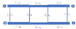
Considering the analytical model of a one-section branch-line coupler [19], the analytical theory is extended to model four-branch BLC. Figure 1 shows a conventional four-branch BLC and its characteristic impedances of through and branch lines. The through lines’ characteristic impedance are and , and their lengths are and respectively. The branch lines’ characteristic impedance is and their length is . Both Port 1 and 4 are excited by in-phase and amplitude of signals which leads to an equivalent open circuit at the line of symmetry. Similarly, two out-of-phase and amplitudes of signals lead to an equivalent short circuit at the line of symmetry. By superposition, the sum of the two cases is a single signal of unit amplitude at Port 1. The resultant signals from the four ports are also the superposition of the results obtained in the even mode and odd mode cases. In each case, the problem reduces to that of a two-port network.
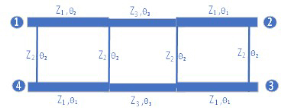
Fig. 1: Four branches of conventional BLC.
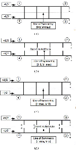
For the even mode, Figs. 2 (a) and (b) show the even mode excitation and the open stubs equivalent circuit, respectively. The even mode ABCD parameters are obtained in Equation (2.1). Similarly, Figs. 2 (c) and (d) show the odd mode excitation and the short stubs equivalent circuit, respectively. The odd mode ABCD parameters are obtained in Equation (2.1).
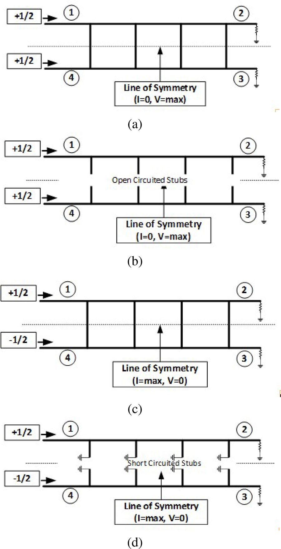
Fig. 2: Decomposition of BLC into (a) even–mode excitation; (b) even–mode equivalent circuit; (c) odd–mode excitation; (d) odd–mode equivalent circuit.
| (1) |
| (2) |
Using ABCD to S parameters transformation [20], and the fact that and , the S-parameter for the four-branch BLC is obtained. The required characteristic impedance, of the branch line for the conventional four-branch, BLC is between 135 and 264 in Butterworth and Chebyshev designs [21]. In [22], the through characteristic impedance and are obtained as Equations (3) and (4).
| (3) |
| (4) |
where the coupling factor is related to and in [4]:
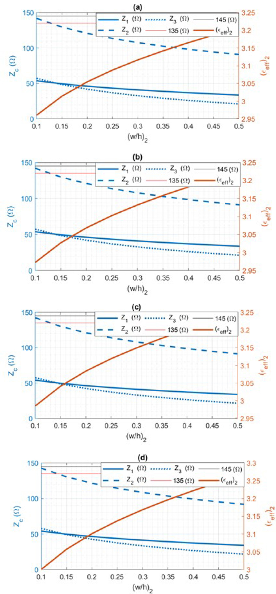
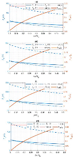
Fig. 3: Characteristic impedances of branch and through lines values at (a) 3 GHz; (b) 4 GHz; (c) 5 GHz; (d) 6 GHz.
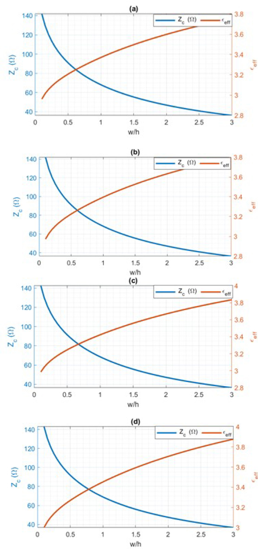
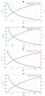
Fig. 4: Characteristic impedances of branch and through lines values versus aspect ratio w/h and effective dielectric constant at (a) 3 GHz; (b) 4 GHz; (c) 5 GHz; (d) 6 GHz.
For physical realizations, the branch characteristic impedance is recommended to be within the range of 135 to 145 . MATLAB code was developed based on this assumption and Equations (3) and (4). Considering the frequency effect (3 GHz – 6 GHz), line-width-to-substrate-height ratio , and the effective dielectric constant , Fig. 3 shows how to choose the through and the branch characteristic impedance values simultaneously, and then choose the aspect ratio and the effective dielectric constant of branch line only. Figure 4 shows the aspect ratio and the effective dielectric constant of the through impedances and at different frequencies. In Table 1, the design process starts by choosing the branch characteristic impedance between 135 to 145 lines shown in Fig. 3 (b) at 4 GHz. is chosen to be 143 with an aspect ratio and . Also, and are found to be 54 and 57.7 , respectively. The through characteristic impedances aspect ratio and effective dielectric constant are extracted from Fig. 4 (b) and are shown in Table 2.
Table 1: Comparison of proposed BLC with previous works
| Ref. | Technique | (dB) |
PE (deg.) | ||
| 13 | Shorted stubs | 3 | 30.5 | 4-10 | 4 |
| 14 | Single section /4 transformer |
3 | 50.9 | 6-14 | 2 |
| 15 | Circular sector patch | 10 | 22.2 | 3-10 | 5 |
| 16 | Impedance varying | 3 | 57 | 3-9 | 5 |
| 17 | Phase inverter | 2 | 48.2 | 3-10 | 5 |
| 18 | Shorted stub and parallel notches | 3.5 | 62 | 9-15 | 4 |
| This work | Circular discs | 3.19 | 103 | 1-12 | 2 |
Table 2: Conventional UWB BLC parameters
| n | ||||
| 2 | 143 | 0.1 | 3.23 | 10.4 |
| 3 | 57.7 | 1.4 | 3.54 | 10 |
| 1 | 54 | 1.59 | 3.58 | 9.9 |
| 0 | 50 | 1.8 | 3.63 | 1.8 |
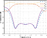
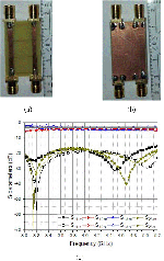
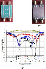
Figure 5 shows the calculated S-parameters of the UWB BLC using the developed MATLAB code. For verification purposes, the conventional UWB BLC is simulated using CST and then fabricated and both measured and simulated results are shown in Fig. 6. Good agreements were obtained between simulated and measured results over the frequency band, which extends from 3.3 GHz to 5 GHz. The conventional UWB coupler has simulated insertion loss and coupling of 3.77 dB and 3.15 dB while the measured insertion loss and coupling of 4 dB and 4.47 dB were obtained. The simulated and measured isolation and return loss are less than 16.5 dB with fractional bandwidth of 56%, and phase imbalances less than over the operating bandwidth.
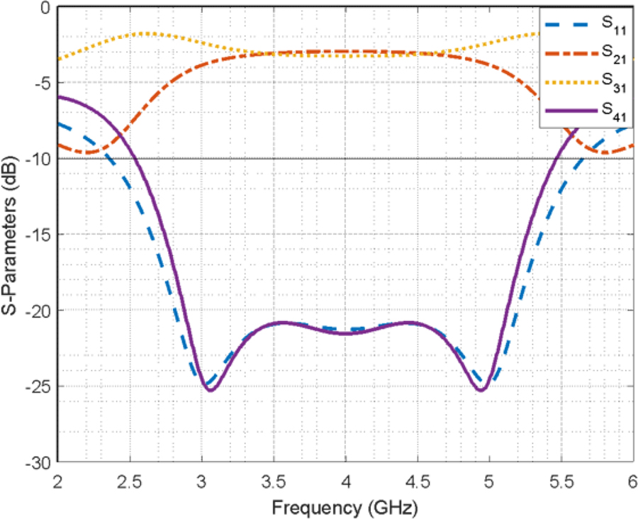
Fig. 5: Calculated S-parameters of conventional UWB BLC.
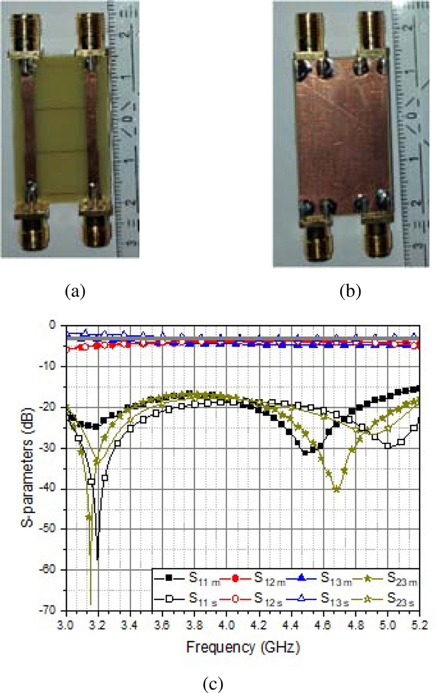
Fig. 6: Conventional UWB BLC (a) fabricated top view; (b) fabricated bottom view; (c) measured and simulated S-parameters.
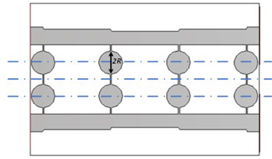
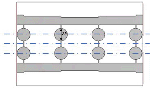
Fig. 7: Proposed UWB BLC with controllable coupling imbalance.
B. Proposed UWB BLC with different coupling imbalance
The UWB BLC coupling is controlled by replacing the uniform branch line with a proposed non-uniform one as shown in Fig. 7. The modified branch line has two circular discs with a radius at its upper and lower centers. As the disc radii increase the coupling imbalance increase. At 4 GHz the coupling imbalance increases from 0.8 dB to 12 dB as radius R increases from 0.25 mm to 1.25 mm, Table 3.
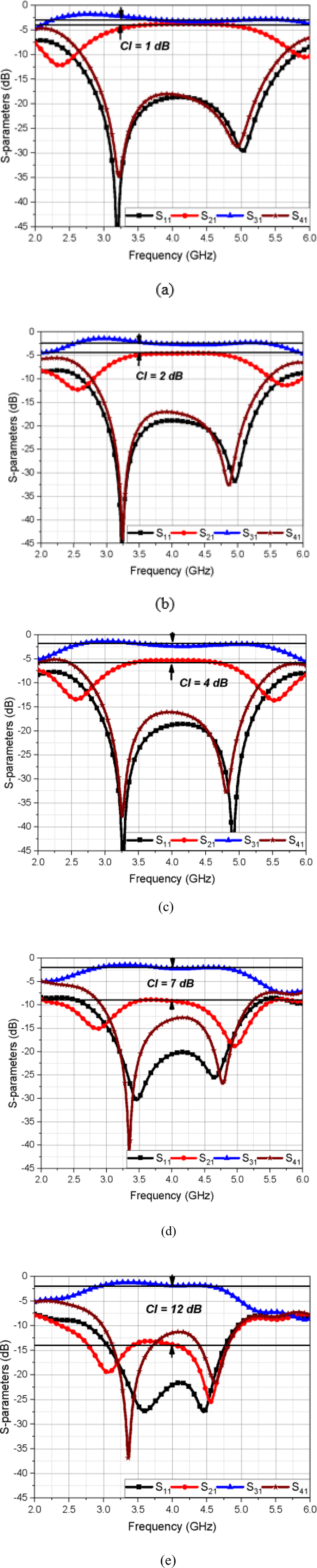
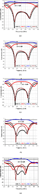
Fig. 8: UWB BLC with controllable coupling imbalance S-parameters at (a) ; (b) ; (c) ; (d) ; (e) .
Table 3: Coupling imbalance values at different disc radii at 4 GHz
| R (mm) | 0.25 | 0.5 | 0.75 | 1 | 1.25 |
| CIR (dB) | 1 | 2 | 4 | 7 | 12 |
Figures 8 (a) to (e) show the S-parameters of the UWB BLC as discs radii increase. The proposed UWB coupler has a coupling imbalance of 1 dB, 2 dB, 4 dB, 7 dB, and 12 dB over the bandwidth which ranges from 3.5 GHz to 5 GHz, 3.75 GHz to 4.65 GHz, 3.6 GHz to 4.5 GHz, 3.64 GHz to 4.2 GHz, and 3.5 GHz to 4 GHz as circular discs have radii of 0.25 mm, 0.5 mm, 0.75 mm, 1 mm, and 1.25 mm, respectively.
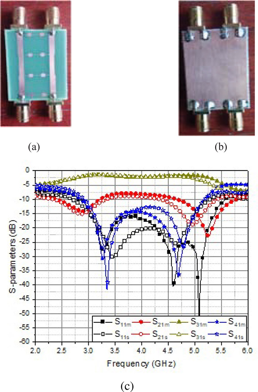
Fig. 9: Proposed fabricated UWB BLC (a) top view; (b) bottom view; (c) measured and simulated S-parameters.
For verification purposes, the proposed UWB BLC with a coupling imbalance of 7 dB is fabricated and measured. The top and bottom views of the proposed fabricated BLC are shown in Figs. 9 (a) and (b), respectively. Both measured and simulated results are shown in Fig. 9 (c). The simulated frequency band with a 7 dB imbalance extends from 3.5 GHz to 4.2 GHz while the measured frequency band with a 7 dB coupling imbalance extends from 3.3 GHz to 4.48 GHz. The simulated insertion loss and coupling of 2.33 dB and 9.33 dB while the measured insertion loss and coupling of 2.2 dB and 8.1 dB are obtained, respectively. The simulated isolation and return loss are less than 13 dB and 20 dB with fractional bandwidth of 20.3%, and phase imbalances less than while the measured isolation and return losses are less than 14 dB and 16 dB with fractional bandwidth of 36%, and phase imbalances less than for the entire operating bandwidth.
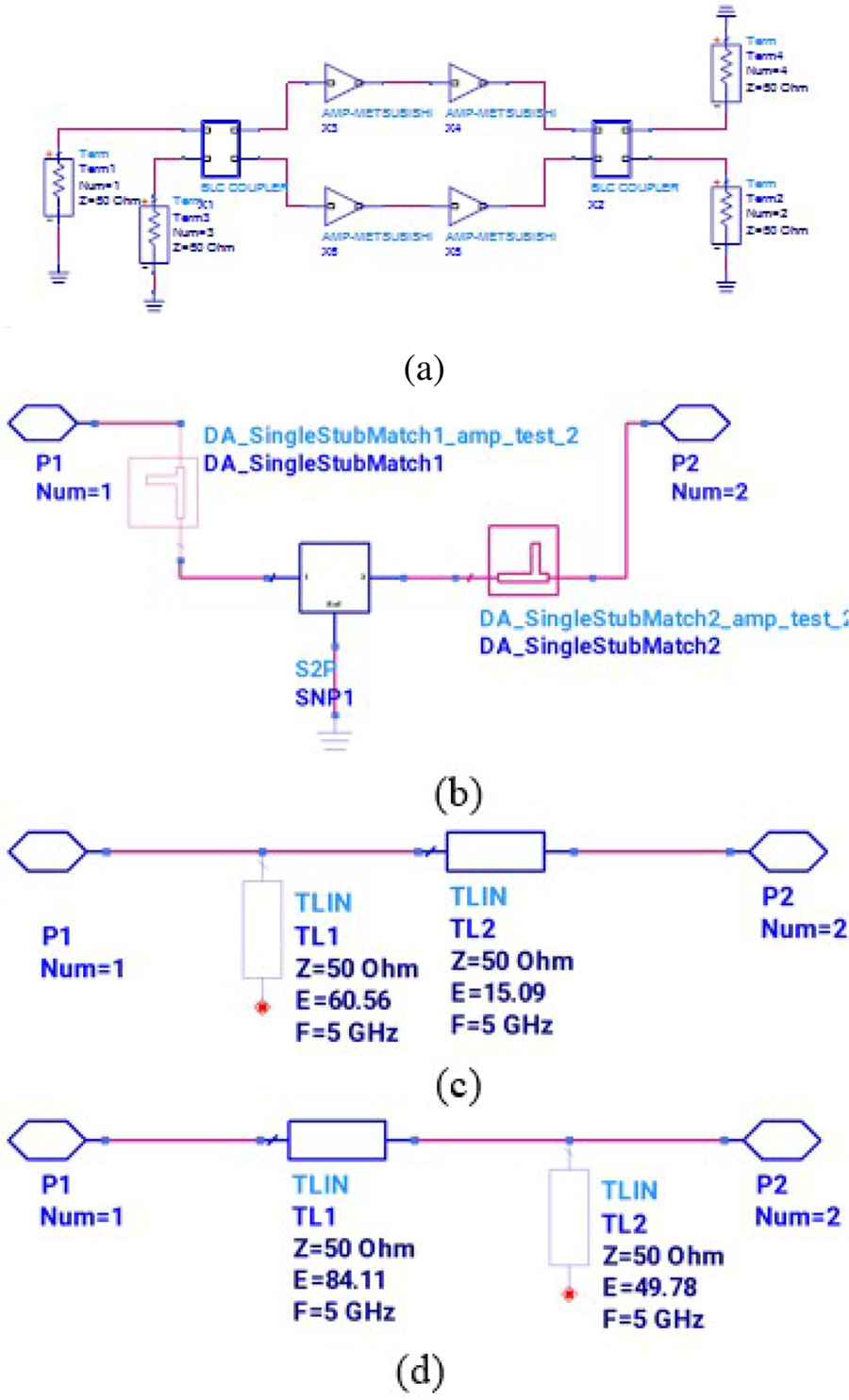
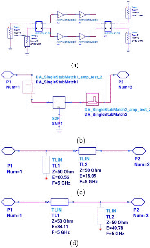
Fig. 10: Proposed UWB LNA (a) circuit diagram; (b) single transistor with input and output matching sections; (c) input matching section; (d) output matching section.
Table 4: factors of the MGF3022AM InGaP-HBT transistor
| 3.00 | 0.863 | 0.692 |
| 3.25 | 0.905 | 0.786 |
| 3.50 | 0.939 | 0.866 |
| 3.75 | 0.976 | 0.95 |
| 4.00 | 1.044 | 1.083 |
| 4.25 | 1.125 | 1.202 |
| 4.50 | 1.234 | 1.287 |
| 4.75 | 1.574 | 1.47 |
| 5.00 | 2.46 | 1.552 |
| 5.25 | 1.743 | 1.738 |
| 5.50 | 1.282 | 1.878 |
| 5.75 | 1.11 | 2.033 |
| 6.00 | 1.04 | 2.112 |
III. BALANCED UWB LNA
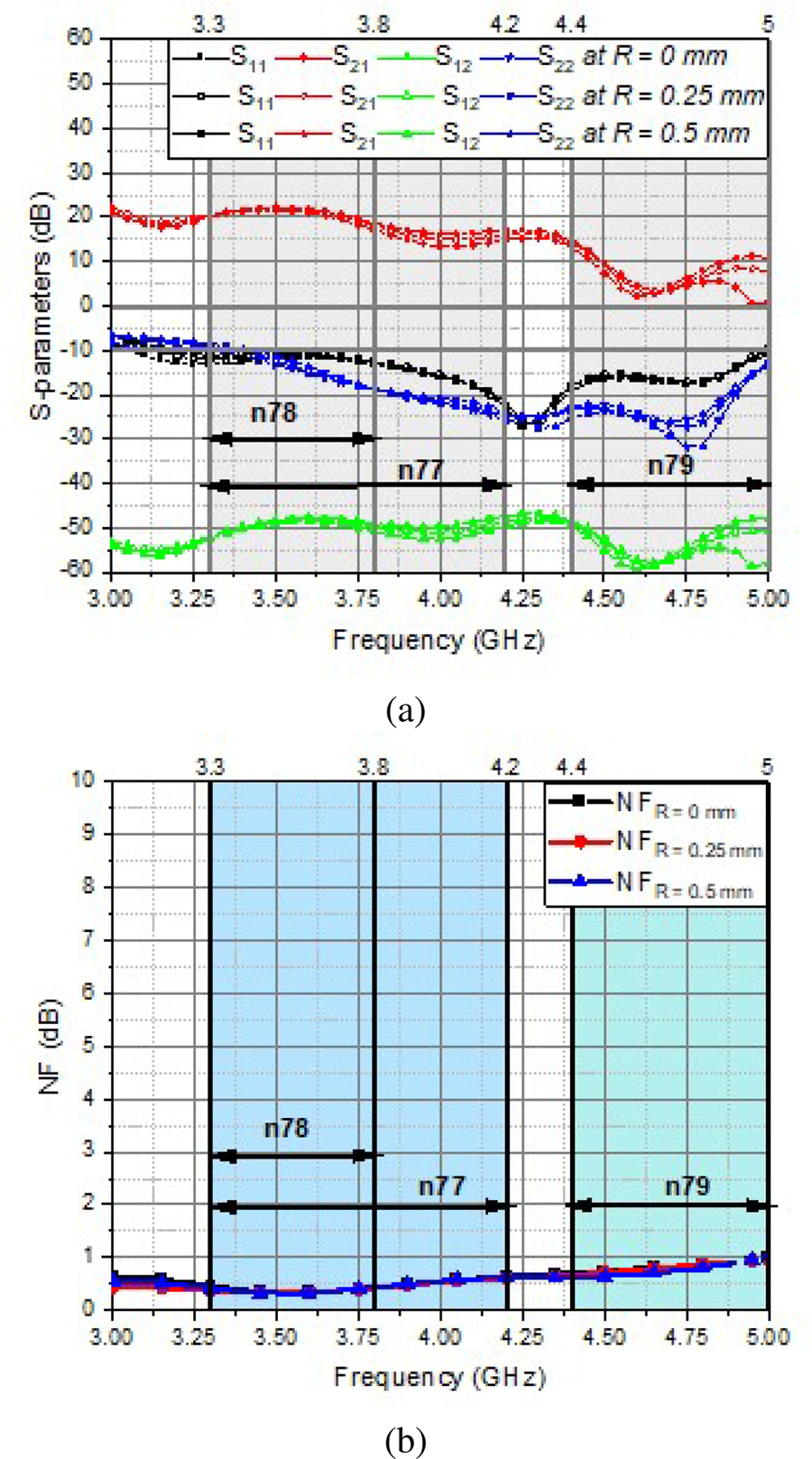
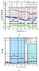
Fig. 11: Proposed LNA circuit (a) S-parameters at different coupling imbalances of the UWB BLC and (b) noise figure at different coupling imbalances of the UWB BLC.
Table 5: LNA parameters for different imbalance coupling associated with different discs’ radii
| R (mm) | I/P RL (dB) |
O/P RL (dB) |
Gain (dB) | NF (dB) | CI (dB) |
| n77 (3.7 GHz) | |||||
| 0 | 11.9 | 17.2 | 19.5 | 0.38 | 0.99 |
| 0.25 | 11.7 | 17 | 20.3 | 0.38 | 2.2 |
| 0.5 | 11.4 | 16.3 | 20.7 | 0.38 | 3.3 |
| 0.75 | 13.2 | 17.8 | 20.1 | 1.1 | 4.1 |
| 1 | 13.3 | 16.9 | 20.6 | 1.1 | 7.2 |
| 1.25 | 14.8 | 16.1 | 21.2 | 1.1 | 11.8 |
| n57 (3.5 GHz) | |||||
| 0 | 11.9 | 13.2 | 21.5 | 0.34 | 1.4 |
| 0.25 | 11.5 | 12.5 | 22.1 | 0.35 | 2.8 |
| 0.5 | 10.7 | 11.5 | 22.3 | 0.32 | 3.8 |
| 0.75 | 12.7 | 11.9 | 20.23 | 1.1 | 4.6 |
| 1 | 11.9 | 10.8 | 19.98 | 0.97 | 7.6 |
| 1.25 | 11.97 | 10.01 | 18.9 | 0.99 | 12.4 |
| n79 (4.7 GHz) | |||||
| 0 | 17.4 | 25.9 | 4.6 | 0.83 | 0.79 |
| 0.25 | 17 | 26.7 | 3.6 | 0.83 | 2.1 |
| 0.5 | 17.2 | 29.1 | 3.7 | 0.74 | 3.8 |
| 0.75 | 16.1 | 22.9 | 8.3 | 1.69 | 5.2 |
| 1 | 18.1 | 20.5 | 6.8 | 1.8 | 11.7 |
| 1.25 | 16.1 | 13.7 | 10.7 | 2.13 | 15.5 |
| 4 GHz | |||||
| 0 | 15.9 | 20.9 | 13.5 | 0.54 | 0.82 |
| 0.25 | 15.8 | 21.8 | 15 | 0.54 | 0.82 |
| 0.5 | 15.5 | 22 | 16.2 | 0.56 | 1.87 |
| 0.75 | 16.3 | 22.8 | 16.8 | 1.34 | 3.85 |
| 1 | 16.9 | 25.3 | 19.1 | 1.29 | 6.96 |
| 1.25 | 20 | 31.8 | 21.11 | 1.26 | 12.13 |
In wireless communication systems, balanced amplifiers have been widely used due to their low noise figure, and better gain and stability as compared to a single amplifier. The proposed LNA circuit consists of four transistors with an impedance-matching network at the input and output of each transistor. MGF3022AM InGaP-HBT (Heterojunction Bipolar Transistor) has opted for the proposed LNA circuit. The MGF3022AM is designed for use in L-to-C-band amplifiers. Additional, two identical UWB BLC with different coupling imbalanced designed in section II are included. Microwave transistors used to design UWB amplifiers are generally not well-matched across the operating frequency band. A wider bandwidth comes at the expense of low gain and more circuit complexity. Thus, we propseda circuit based on four amplifiers having a UWB coupler to provide a good adaptation for the gain and bandwidth. ADS simulator is used as a CAD tool to analyze the circuit performance. The balanced amplifier circuit is shown in Fig. 10 (a). Figure 10 (b) shows the transistor block, which has S-parameters of and , and it’s matching input and output circuits. Figures 10 (c) and (d) shows the equivalent input and output transmission line matching circuits designed at , where is the line impedance in and is the electrical length of the open stub in degree. Table 4 shows the and factors of the MGF3022AM InGaP-HBT transistor after adding the input and output matching sections. The and factors are given by [5] as:
| (5) |
The amplifier is nearly unconditionally stable across the 5G operating frequency band.
Different coupling imbalances associated with different discs’ radii of UWB BLCs are used for the balanced LNA performance analysis. Figure 11 (a) shows the input return loss, output return loss, gain, and isolation for the first three coupling imbalances associated with the first three discs’ radii of BLC balanced. Figure 11 (b) shows the associated noise figure of balanced LNA. Table 5 shows different LNA parameters for imbalances associated with six different discs’ radii. For the 5G n77 center band, the gain varies from 19.5 dB to 21.2 dB while NF is better than 1.1. The input and output return loss, are better than 11.4 dB. For the 5G n57 center band, the gain varies from 18.9 dB to 22.3 dB, while NF is better than 1.1. The input and output return loss are better than 10 dB. For the 5G n79 center band, the gain varies from 3.6 dB to 10.7 dB, while NF is better than 2.3. The input and output return loss are better than 13.7 dB. Additionally, at 4 GHz (the center frequency of the UWB BLC), the gain varies from 13.5 dB to 21.11 dB while NF is better than 12.13. The input and output return loss are better than 15.5 dB.
IV. CONCLUSION
We introduced a simple and new method of controlling the coupling imbalance of the UWB BLC. For verification, a conventional UWB BLC was designed, fabricated, and measured. Additionally, a UWB BLC with a coupling imbalance of 7 dB was designed, fabricated, and measured. Both UWB BLC and UWB BLC with a 7 dB coupling imbalance were measured and simulated, and their results were founded to be in good harmony. The application of the proposed LNA-design BLC was verified. The proposed BLC added a degree of freedom in the design of the LNA considering gain and NF.
The UWB LNA that uses UWB BLC with an imbalance coupling is suitable for 5G sub6 GHz applications as well as other wireless communication systems such as navigation and radar applications.
REFERENCES
[1] T. G. Abouelnaga, I. Zewail, and M. Shokair, “Design of 10 10 massive MIMO array in sub-6 GHz smartphone for 5G applications,” Progress in Electromagnetics Research B, vol. 91, pp. 97-114, 2021.
[2] I. Al-Mejibli and S. Al-Majeed, “Sub-6 GHz quad-band reconfigurable antenna for 5G cognitive radio applications challenges of using MIMO channel technology in 5G wireless communication systems,” Applied Computational Electromagnetics Society (ACES) Journal, vol. 36, no. 8, pp. 1015-1025, 2021.
[3] A. Junuthula and A. Prakasa, “A dual band AMC backed antenna for WLAN, WiMAX, and 5G wireless applications,” Applied Computational Electromagnetics Society (ACES) Journal, vol. 36, no. 9, pp.1209-1214, 2021.
[4] A. Biswas and G. Vibha, “Design and development of low-profile MIMO antenna for 5G new radio smartphone applications,” Wireless Personal Communications, vol. 111, no. 3, pp. 1695-1706, 2020.
[5] 5G NR specifications, document TS 38.101-1 V15.4.0 3GPP Release 15, 2018.
[6] R. S. Kshetrimayum, “An introduction to UWB communication systems,” IEEE Potentials, vol. 28, pp. 9-13, 2009.
[7] D. K. Misra, Radio Frequency and Microwave Communication Circuits; Analysis and Design, John Wiley & Sons, 2004.
[8] C. Y. Pon, “Hybrid-ring directional coupler for arbitrary power division,” IEEE Trans. Microw. Theory Tech., vol. 19, no. 11, pp. 529-535, 1961.
[9] R. Levy and L. J. Lind, “Synthesis of symmetric branch line guide directional couplers,” IEEE Trans. Microw. Theory Tech., vol. 16, no. 12, pp. 80-89, 1968.
[10] G. L. Matthaei, L. Young, and E. M. T. Jones, Microwave Filters, Impedance-Matching Network, and Coupling Structures, Norwood, MA, Artech House, 1980.
[11] A. K. Agrawal and G. F. Mikucki, “A printed-circuit hybrid-ring directional coupler for arbitrary power divisions,” IEEE Trans. Microw. Theory Tech., vol. 34, no. 12, pp. 1401-1407, Dec. 1986.
[12] C. Hsu, J. Kuo, and C. Chang, “Miniaturized dual-band hybrid couplers with arbitrary power division ratios,” IEEE Transactions on Microwave Theory and Techniques, vol. 57, no. 1, pp. 149-156, 2009.
[13] Z. Qamar, S. Y. Zheng, W. S. Chan, and D. Ho, “Coupling coefficient reconfigurable wideband branch-line coupler topology with harmonic suppression,” IEEE Transactions on Microwave Theory and Techniques, vol. 66, no. 4, pp. 1912-1920, 2018.
[14] S. Lee and Y. Lee, “Wideband branch-line couplers with single-section quarter-wave transformers for arbitrary coupling levels,” IEEE Microwave and Wireless Components Letters, vol. 22, no. 1, pp. 19-21, Jan. 2012.
[15] S. Y. Zheng, J. H. Deng, Y. M. Pan, and W. S. Chan, “Circular sector patch hybrid coupler with an arbitrary coupling coefficient and phase difference,” IEEE Transactions on Microwave Theory and Techniques, vol. 61, no. 5, pp. 1781-1792, 2013.
[16] K. A. Alshamaileh, V. K. Devabhaktuni, and N. I. Dib, “Impedance-varying broadband 90 branch-line coupler with arbitrary coupling levels and higher order harmonic suppression,” IEEE Transactions on Components, Packaging and Manufacturing Technology, vol. 5, no. 10, pp. 1507-1515, 2015.
[17] L. Chiu and Q. Xue, “Investigation of a wideband 90-degree hybrid coupler with an arbitrary coupling level,” IEEE Transactions on Microwave Theory and Techniques, vol. 58, no. 4, pp. 1022-1029, 2010.
[18] Q. Zeeshan, S. Y. Zheng, W. S. Chan, and H. Derek, “Coupling coefficient range extension technique for broadband branch-line coupler,” Journal of Electromagnetic Waves and Applications, vol. 32, no. 1, pp. 92-112, 2018.
[19] T. G. Abouelnaga and A. S. Mohra, “Reconfigurable 3/6 dB novel branch line coupler,” Open Journal of Antennas and Propagation, vol. 5, no. 1, pp. 1-7, 2017.
[20] M. Pozar, Microwave Engineering, John Wiley & Sons, 2011.
[21] M. Muraguchi, T. Yukitake, and Y. Naito, “Optimum design of 3-dB branch-line couplers using microstrip lines,” IEEE Trans. Microw. Theory Tech., vol. 31, no. 8, pp. 674-678, 1983.
[22] W. Yongle, J. Shen, and Y. Liu, Comments on “Quasi-Arbitrary Phase-Difference Hybrid Coupler,” IEEE Trans. Microw. Theory Tech., vol. 61, no. 4, pp. 1725-1727, 2013.
BIOGRAPHIES

Tamer Gaber Abouelnaga was born November 1976. He received his B.Sc. degree (1994–1999, honors degree) in Electronics Engineering from Menofiya University, Egypt, and M.Sc. (2002–2007) and Ph.D. degrees (2007–2012) in Electronics and Communications from Ain Shams University, Egypt. He works at Microstrip Circuits Department, Electronics Research Institute, Egypt as a Researcher (2012–2017) and an Associate Professor (2018 to present). He also has worked as the Students Affairs Vice Dean (2018–2019) and the Community Service, Environmental Development Vice Dean (2019–2022) – Higher Institute of Engineering and Technology – Kafr Elsheikh City, as well as the Students Affairs Vice Dean (2022–2023) – College of Industry and Energy Technology, New Cairo Technological University (NCTU), Egypt. He has published 42 papers, 29 papers in peer-reviewed journals, and 13 papers in international conferences regarding antennas, couplers, filters, and dividers for different microwave applications.
Esmat A. Abdallah (Senior Member, IEEE) graduated from the Faculty of Engineering, Cairo University, Giza, Egypt in 1968. She received her M.Sc. and Ph.D. degrees from Cairo University in 1972 and 1975, respectively. She was nominated as an Assistant Professor, Associate Professor, and Professor in 1975, 1980, and 1985, respectively. In 1989, she was appointed President of the Electronics Research Institute (ERI), Cairo, Egypt, a position she held for approximately 10 years. She then became the Head of the Microstrip Department, ERI, from 1999 to 2006. Currently, she is at the Microstrip Department, Electronics Research Institute, Cairo, Egypt. She focuses on her research on microwave circuit designs, planar antenna systems, and nonreciprocal ferrite devices, and recently on EBG structures, UWB components, and antenna and RFID systems. She has been a single author or co-author on more than 285 research papers in highly cited international journals and proceedings of international conferences. She has 6 books and 7 patents. She supervised more than 85 Ph.D. and M.Sc. theses. She is a member of the National Council of Communication and Information Technology.
ACES JOURNAL, Vol. 37, No. 9, 986–995.
doi: 10.13052/2022.ACES.J.370908
© 2022 River Publishers