Super-Broadband Rectifier with Wide-band Resistance Compression Network and Harmonic Cycling for RF-Harvesting
Xin Liu, Dawei Zhang, Yingsong Li, and Zhixiang Huang
1College of Information and Communication Engineering
Harbin Engineering University, Harbin, 150001, China
2Key Laboratory of Intelligent Computing and Signal Processing
Ministry of Education, Anhui University, Hefei, 230601, China
liyingsong@ieee.org
3Anhui Province Key Laboratory of Target Recognition and Feature Extraction
LuAn, 230088, China
Submitted On: July 11, 2022; Accepted On: August 14, 2022
ABSTRACT
In this paper, a super-broadband (SBB) rectifier using a wideband resistance compression network (WRCN) and harmonic cycling is proposed, simulated, fabricated, measured and analyzed in detail for the harvesting of ambient radio frequency (RF) energy. Meanwhile, impedance compression and matching are achieved to implement the SBB using WRCN and impedance operation networks. Additionally, harmonic cycling structure and bending technology are employed to improve the power conversion efficiency (PCE) and reduce the size, respectively. For demonstration, a prototype of the proposed rectifier is fabricated and measured. The measured results are in good accordance with the simulated ones, indicating that the rectifier can provide high efficiency and ultra-broadband rectification characteristics. A PCE over 50 is realized at 3.5 GHz with an input power range of 6–24 dBm, and a PCE of 75 is obtained at an input power of 18 dBm. The PCE is greater than 50 at 17 dBm with an input frequency of 2.7-4.6 GHz. This work can find significant applications in the development of RF-harvesting.
Index Terms: bending technique, harmonic cycling, RF-harvest, super-Broadband rectifier, wide-band resistance compression technique.
I. INTRODUCTION
With the rapid development of communication technologies, human beings’ living surroundings are full of electromagnetic waves. If these electromagnetic energies can be recycled and harvested on the spot, we can get rid of the limitation that their batteries determine the lifetime of electronic devices. Consequently, radio frequency (RF)-harvest is currently attracting much attention in scientific and industrial fields. Various RF-harvest devices are currently used in the medical field, smart homes, electric vehicles, consumer electronics, and drone charging [1]. Many rectifiers can now achieve high power conversion efficiency (PCE) in narrow band ranges. However, with the rise of 5G and Internet of Things (IoT) technologies and MIMO radars [2], wider bands are being used for wireless communications where the electromagnetic energy is distributed across multiple bands. Therefore, it is becoming increasingly important to design broadband rectifiers to maximize the amount of power that can beharvested [3, 4].
A lot of rectifiers have been reported to address these mentioned problems. A rectifier consisting of a two-stage coupler is proposed and discussed in [5], which allows the reflected power caused by impedance mismatch to be re-rectified, improving the rectification efficiency, and a fractional bandwidth of 21.5 and a PCE over 70 have been achieved from 2.08 GHz to 2.58 GHz. The rectifier in [6] uses a non-uniform transmission line to achieve broadband rectification characteristics, resulting in a PCE higher than 50 over a bandwidth of 0.4–1 GHz. In [7], a two-stage impedance matching network was used to achieve a PCE greater than 50 with a fractional bandwidth over 37 (1.8–2.72 GHz). In [8], by using a taper impedance matching network, a broadband rectifier is achieved over 2–3.05 GHz with an input power of 10 dBm, and a peak PCE of 75.8 is obtained at an input power of 14 dBm. There are other methods to increase the operating bandwidth of rectifiers by using sub-rectifiers operating in a different band range[9, 10]. In addition, the PCE can be improved by increasing the matching quality using varactor diodes andMOSFETs given in [10, 11]. However, it is still a great challenge to design rectifiers to cover multiple frequency bands.
This paper proposes an ultra-broadband rectifier with a wideband resistance compression network (WRCN) and harmonic cycling for RF-harvesting to address this issue. Two branches are connected using WRCN to achieve wideband impedance matching. The PCE of the rectifier is further improved with broadband, and a harmonic cycling technique is considered to achieve a broadband high-efficiency rectifier. The proposed rectifier is designed to get a PCE greater than 50 at an input power of 17 dBm from 2.7 to 4.6 GHz, which has a fractional bandwidth over 65 and provides a peak PCE up to 75 at 3.5 GHz with an input power of 18 dBm.
II. THEORETICAL ANALYSIS OF THE RECTIFIER
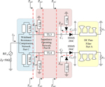
Figure 1 is the schematic diagram of the designed super-broadband (SBB) rectifier for RF energy harvesting applications using WRCN and harmonic cycling. The SBB rectifier circuit consists of two load resistors, a DC-pass filter (part A), two HSMS286C Schottky diodes, an impedance operating network (part B) and a wideband WRCN (part C).
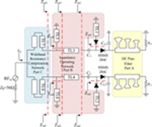
Figure 1: Schematic of the proposed super-broadband rectifier.
A. Design of the DC-pass filter and harmonic cycling
Since the Schottky diode is a non-linear component, it would generate fundamental frequency and high harmonics in the process of converting the RF signal to DC signal, while the high harmonics are mainly dominated by the second harmonic, and the rest of the high harmonics carry too little energy that can be negligible. In order to make the output voltage more stable, DC-pass filters combine lumped and distributed elements in this design, which is to smooth the output DC waveform and return the fundamental and higher harmonics to the Schottky diode for re-rectification.
The harmonic cycling structure in the proposed broadband rectifier consists of three linear microstrip stubs and three fan-shaped microstrip stubs. As depicted in Fig. 2, a fan-shaped stub has two characteristic parameters: the radius and the angle . The input impedance of the fan-shaped stub can be calculated from equations (1), (2), (3) and (4) [12]:
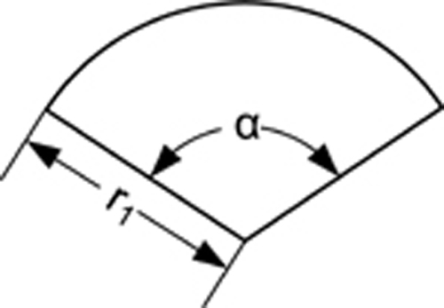
Figure 2: Characteristic parameters of the fan-shaped stub.
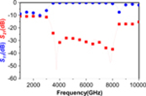
Figure 3: The simulated S-parameters of harmonic cycling.
| (1) |
| (2) |
| (3) |
| (4) |
where , , , represent the first class of 0-order Bessel function, the second class of 0-order Bessel function, the first class of 1-order Bessel function and the second class of 1-order Bessel function, respectively. denotes the wavelength in free space, is the equivalent dielectric constant, and h is the thickness of the dielectric substrate. In addition, the resonance point of the input impedance of the fan-shaped stub is less affected by frequency variations than that of the linear stub. Thus, the smoother return loss curve of the fan-shaped stub provides a broader bandwidth, which also exhibits a wider stop band in the DC-pass filter. Here, the DC-pass filter mainly consists of fan-shaped stubs and linear stubs, with the fan-shaped stubs to reduce the longitudinal size and the linear stubs to avoid the problem of the excessive transverse size of the fan-shaped stubs. The S-parameter is presented in Fig. 3, showing that the designed DC-pass filter can suppress the fundamental and higher harmonics of the RF signal and ensure a smooth DC output.
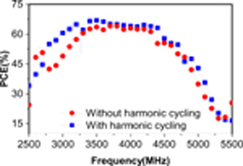
Figure 4: Comparison of the PCE with and without the harmonic cycling structure.
A comparison of the PCE with and without harmonic loop structure at an input power of 15 dBm is shown in Fig. 4, where the DC-pass filter can recover fundamental and second harmonics over a wide frequency range and improve the PCE. Furthermore, since the filter will be integrated into the circuit, there will be inevitable interactions with the other structures. Therefore, the parameters of the DC-pass filter structure should be adjusted to be optimal for the entire rectifier circuit design.
B. Design of an impedance operation network (ION)
In this design, an ION is used to convert the complex impedance into a wide resistance . The upper and lower branches in the ION have the same structures, which both consists of two short-circuit stubs TL1 (TL2), TL5 (TL6) and a section of microstrip transmission line TL3 (or TL4). Thus, the upper branch is used as an example to discuss the operating principle and parameters in this section.
Firstly, the upper branch of the ION consists of two short-circuit stubs TL1, TL5 and a section of microstrip transmission line TL3, where TL1 is mainly to counteract the capacitive characteristics carried by parallel branch diodes. Since the diode is mainly capacitive in its operating range, TL1 is used as a short-circuit inductor to compensate for the capacitive characteristics of the diode in the operating band by connecting the inductive and capacitive in series. The characteristic impedance and electrical length of TL1 are and , respectively. The input impedance of the diode in parallel is denoted as =+. Then, the input impedance of the branch after series connection with TL1 can be described as:
| (5) |
In order to better understand the design, we define the operating band as (, ), where < and /=, which can be further denoted as ()=()=. Under ideal circumstances, TL1 should compensate for the capacitive characteristic of caused by the diodes in parallel branch with frequency ranging from to , and hence, the characteristic impedance and electrical length of TL1 for a specific power can be calculated using:
| (6) |
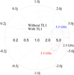
The TL1 can reduce the input impedance variation of the two diodes in the operating bandwidth and provide a basis for further impedance compression. The diode used in this design is the HSMS286C, and we integrate two diodes into one package. After optimization in Advanced Design Simulation (ADS) with Harmonic Balance Simulation (HB), the characteristic impedance and electrical lengths of TL1(TL2) is calculated at 3.5 GHz to be =81 , =41.2 deg. At an input power of 17 dBm, the input impedance is shown in Fig. 5 after using the series short-circuit stub TL1(TL2), which is equivalent to an inductor, to cancel the diode capacitance.

Figure 5: Comparison of with and without TL1.
Secondly, the microstrip transmission line TL3 has the role of adjusting the imaginary part of the rectifier’s input impedance after TL1. To calculate the characteristic impedance and electrical length of the series microstrip transmission line TL3, the rectifier initial input impedance at and is expressed as ()=+ and ()=+. Then, the rectifier input impedance at and after TL3 can be obtained and is given by equations (7) and (8):
| (7) |
| (8) |
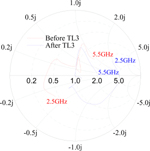
The characteristic impedance and electrical length of TL3(TL4) were calculated to be =77 , =153 deg at 3.5 GHz. () and () in the equations can be obtained using ADS simulation. Figure 6 shows the input impedance of the rectifier in the 2.5–5.5 GHz band. It is observed that at an input power of 17 dBm, the real part of in the frequency band of interest is approximately 39–50 , and the imaginary part nearly oddly symmetrical about the 3.5 GHz frequency. In addition, a bending technique has been adopted in this design, which greatly reduces the space occupied by the TL3, saving space and reducing manufacturing costs.
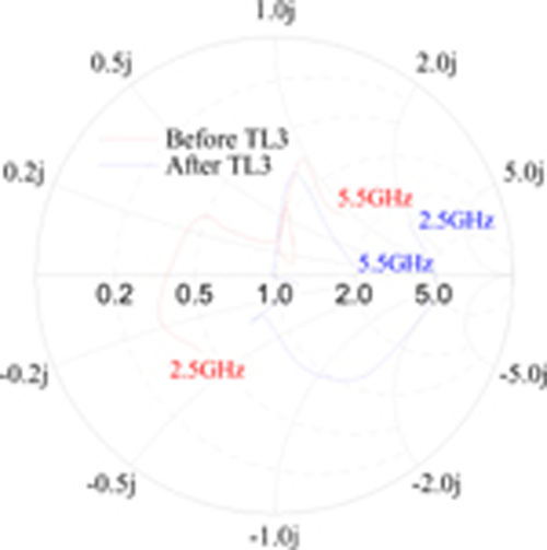
Figure 6: Comparison of before and after TL3.
Thirdly, the input impedance of the rectifier is further compressed by TL5, which compresses the complex impedance into a wide resistance. Calculating the electrical length and characteristic impedance of TL5, the inductance of the rectifier input impedance at and is expressed as -, +, respectively. Then, the inductance at and after TL5 is expressed as:
| (9) |
| (10) |
The characteristic impedance and electrical length of TL5(TL6) were calculated to be =77 , =79.7 deg at 3.5 GHz. Combining the two above equations gives the characteristic impedance and electrical length of TL5. Further compression is applied to the input impedance to get oddly symmetric about the resistance axis. Compared to the graph before compression, the compressed input impedance only varies around the resistive axis of the Smith chart. It is worth noting that the proposed ION can also work over a wide range of input powers since the input impedance of a Schottky diode rectifier varies with the input power and has a similar trend in the bandwidth.
C. Design of a WRCN
In this section, a WRCN is used to achieve impedance matching of the rectifier over broadband. The precondition for using WRCN is that the rectifier should have two branches. The principle behind it lies in the use of two transmission lines with electrical lengths of + and -, respectively, which can reduce the fluctuation of the input impedance due to load changes when it is connected in parallel. Compared to impedance compression networks, RCN requires additional ION, and impedance manipulation networks can transform complex impedances into wide resistances over a wide frequency range to a more stable achieve impedance matching over broadband.
The idea of designing the WRCN is presented as follows. Firstly, the WRCN should provide a resistor in the broadband, which is obtained from the previous ION analysis. For a conventional microstrip linear resistive compression network, it is difficult for the two branches to maintain complementary electrical lengths in the broadband, which can be well solved by using a double coupled line. Let the coupled line TL7 have an even-mode (odd-mode) characteristic impedance of () and an electrical length of at and at . Regarding the coupled line as a section of the transmission line, the characteristic impedance of this transmission line is , while the electrical lengths at and are and , respectively. To achieve complementarity of electrical lengths, and should satisfy:
| (11) |
Then, the ABCD transmission matrix of the coupled line at is modeled as equations (12), (13) and (14):
| (12) |
| (13) |
| (14) |
Similarly, the equivalent ABCD transmission matrix of the coupling line at can be obtained. The characteristic impedance and electrical lengths for the coupled line can be calculated using the above four equations, where the electrical lengths operating at and have a relationship of =×. The characteristic impedance and electrical length for TL6 can be obtained using the same analysis, except that the equivalent electrical length of TL6 at is that equals to (-), and the equivalent electrical length at is . In addition, the parallel impedance of the two branches is 50 , which matches the source impedance.
III. IMPLEMENTATION AND MEASUREMENT RESULTS
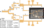
Based on the above principle analysis, the layout of the proposed rectifier is modelled in ADS and jointly optimized, which is shown in Fig. 7. The rectifier is printed on a F4B (=2.55, tan=0.002) dielectric substrate with thickness of h=0.762 and a total size of 94×60 . Herein, two HSMS2862C are used as rectifier diodes, and the capacitors are all Murata’s GRM18 series 100 pf capacitors, and the load resistance is 650 . To facilitate adjustment, two experimental resistor boxes are used in the test. Alternatively, if it was preferred to use only one load, the resistance value of the replacement load should be twice the resistance value of the initial load, and the PCE would remain almost unchanged.
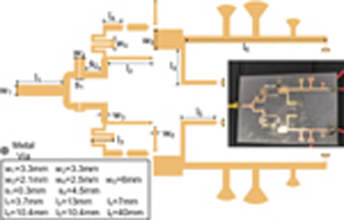
Figure 7: Layout of the proposed rectifier.
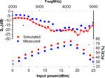
In the experiment, an Agilent PNA-X vector network analyzer is used as a signal source, two adjustable resistor boxes are used as load resistors, and a multimeter is used to measure the output voltage. The proposed ultra-broadband rectifier is analyzed, fabricated and tested. Figure 8 gives a comparison of the simulated of the proposed rectifier with the measured results at an input power of 17 dBm, showing that the rectifier has a good broadband characteristic. Herein, the PCE is calculated using equation (15) [13, 14]:
| (15) |
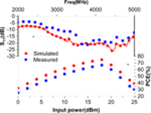
Figure 8: (Upper lines) Measured and simulated of the rectifier. (Lower lines) Measured and simulated PCE versus input power at 3.5 GHz.
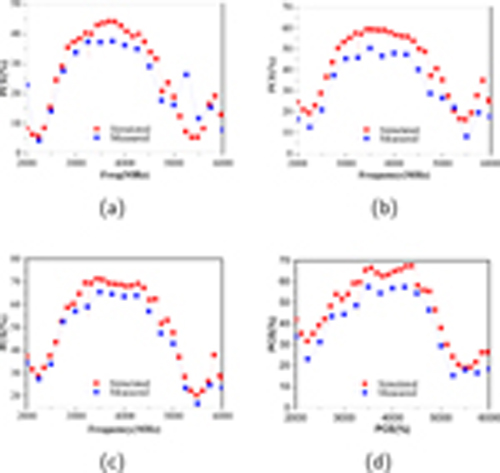
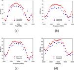
Figure 9: Measured and simulated PCE variations at different input power levels (a) 5 dBm, (b) 10 dBm, (c) 17 dBm, and (d) 20 dBm.
Table 1: Comparison between the suggested rectifier and related designs
| Ref. | Freq.(GHz) | FBW. | Max-PCE | Size() |
| [5] | 2.08–2.58 | 20.8 | 80.8 | 12668 |
| [8] | 2–3.05 | 41.5 | 75.8 | — |
| [15] | 0.915 | — | 74.2 | — |
| [16] | 1.7–2.9 | 50 | 76 | 5636 |
| This work | 2.7–4.6 | 52 | 75 | 9460 |
Figure 9 presents the simulated PCE versus measured PCE for input powers at 5 dBm, 10 dBm, 17 dBm, 20 dBm, respectively. From the results, we found that there is a maximum band range of 2.7-5 GHz at an input power of 17 dBm with PCE>50.
Figure 8 shows the simulated and measured PCE variation with input power at a frequency of 3.5 GHz. We can see that the maximum conversion efficiency of 77 is obtained when the input power is 19 dBm, and a PCE>50 is achieved with an input power of 6-24 dBm. Table 1 shows a comparison between the proposed rectifier and some previous similar works. The proposed rectifier has the widest bandwidth and balanced PCE. The difference between the experimental and simulated results is mainly caused by soldering errors and insertion losses of the SMA connectors.
IV. CONCLUSION
A super-broadband rectifier using a WRCN and harmonic cycling is proposed for RF-harvesting. Impedance matching over a wide bandwidth is achieved by using an impedance operation network consisting of three microstrip lines and a WRCN designed via coupled lines. The harmonic cycling structure further improves the PCE of the rectifier, while the bending technique is used to reduce the size of the rectifier. The proposed rectifier achieves a PCE over 50 from 2.7-4.6 GHz at an input power of 17 dBm, and the designed rectifier has a fractional bandwidth of over 50. The techniques described in this work can also apply to other rectifier circuits.
REFERENCES
[1] X. Sun, C. Liu, Y.-D. Chen, J. Jing, Z. He, and P. Wu, “Low-power wireless uplink utilizing harmonic with an integrated rectifier-transmitter,” IEEE Microw. Wirel. Compon. Lett., vol. 31, no. 2, pp. 200-203, Feb. 2021.
[2] W. Shi, X. Liu, and Y. Li, “ULA fitting for MIMO radar,” IEEE Comm. Lett., vol. 26, no. 9, pp. 2190-2194, Sep. 2022.
[3] W. Liu, K. Huang, T. Wang, Z. Zhang, and J. Hou, “A broadband high-efficiency RF rectifier for ambient RF energy harvesting,” IEEE Microw. Wirel. Compon. Lett., vol. 30, no. 12, pp. 1185-1188, Dec. 2020.
[4] X. Liu, D. W. Zhang, Y. Li, and T. Jiang, “Low power broadband rectifier with wide dynamic input power range for RF-harvesting,” IEEE AP-S/URSI, Denver, USA, 2022.
[5] X. Y. Zhang, Z. Du, and Q. Xue, “High-efficiency broadband rectifier with wide ranges of input power and output load based on branch-line coupler,” IEEE Trans. Circuits Syst. I-Regul. Pap., vol. 64, no. 3, pp. 731-739, Mar. 2017.
[6] H. Sakaki and K. Nishikawa, “Broadband rectifier design based on quality factor of input matching circuit,” Proc. Asia-Pacific Microw.Conf., Sendai, Japan, pp. 1205-1207, Nov. 2014.
[7] C. Song, Y. Huang, P. Carter, J. Zhou, S. Yuan, Q. Xu, and M. Kod, “A novel six-band dual CP rectenna using improved impedance matching technique for ambient RF energy harvesting,” IEEE Trans. Antennas Propag., vol. 64, no. 7, pp. 3160–3171, Jul. 2016.
[8] P. Wu, S. Y. Huang, W. Zhou, W. Yu, Z. Liu, X. Chen, and C. Liu, “Compact high-efficiency broadband rectifier with multi-stage-transmission-line matching,” IEEE Trans. Circuits Syst. II: Express Briefs, vol. 66, no. 8, pp. 1316-1320, Aug. 2019.
[9] C. Li and T. Lee, “2.4-GHz high-efficiency adaptive power,” IEEE Trans. Very Large Scale Integr. (VLSI) Syst., vol. 22, no. 2, pp. 434-438, Feb.2014.
[10] V. Marian, B. Allard, C. Vollaire, and J. Verdier, “Strategy for microwave energy harvesting from ambient field or a feeding source,” IEEE Trans. Power Electron., vol. 27, no. 11, pp. 4481-4491, Nov. 2012.
[11] Z. Liu, Z. Zhong, and Y. Guo, “Enhanced dual-band ambient RF energy harvesting with ultra-wide power range,” IEEE Microw. Wirel. Compon. Lett., vol. 25, no. 9, pp. 630-632, Sep. 2015.
[12] S. L. March, “Analyzing lossy radial-line stubs (short papers),” IEEE Trans. Microw. Theory Tech., vol. 33, no. 3, pp. 269-271, Mar. 1985.
[13] J. Kim and J. Oh, “Compact rectifier array with wide input power and frequency ranges based on adaptive power distribution,” IEEE Microw. Wirel. Compon. Lett., vol. 31, no. 5, pp. 513-516, May 2021.
[14] W. Liu, K. Huang, T. Wang, J. Hou, and Z. Zhang, “A compact high-efficiency RF rectifier with widen bandwidth,” IEEE Microw. Wirel. Compon. Lett., vol. 32, no. 1, pp. 84-87, Jan. 2022.
[15] G. Song, X. Liu, and C. Liu, “Wide-range rectifier for wireless power transfer based on power compensation,” IEEE Microw. Wirel. Compon. Lett., vol. 31, no. 5, pp. 509-512, May 2021.
[16] Z. Du, S. F. Bo, Y. F. Cao, J. Ou, and X. Y. Zhang, “Broadband circularly polarized rectenna with wide dynamic-power-range for efficient wireless power transfer,” IEEE Access, vol. 8, pp. 80561-80571, Apr. 2020.
BIOGRAPHIES

Xin Liu was born in Gansu, China. He received the B.S. degree in Optoelectronic Information Science and Engineering from the North University of China, Shanxi, China, in 2019. He is currently pursuing the M.S. degree in Electronics Information with the Harbin Engineering University, China. His current research interests include RF circuit design, antenna design, wireless power transmission.

Dawei Zhang receieved the B.S. and M.S. degree from the University of Electronic Science and Technology of China, Chengdu, China, in 2011 and 2014, respectively, and the Ph.D. degree from Harbin Institute of Technology, Harbin, China, in 2019.
In 2019, he joined the College of Information and Communication Engineering, Harbin Engineering University, as an assistant professor. His current research interests include metamaterials and spoof surface plasmon polaritons.

Yingsong Li received his B.S. degree in Electrical and Information Engineering, and M.S. degree in Electromagnetic Field and Microwave Technology from Harbin Engineering University, 2006 and 2011, respectively. He received his Ph.D degree from both Kochi University of Technology (KUT), Japan and Harbin Engineering University (HEU), China in 2014. He is currently a Full Professor with the School of Electronic and Information Engineering of Anhui University from March 2022. He was a full Professor in Habirn Engineering University from 2014 to 2022 and a visiting scholar of University of California, Davis from March 2016 to March 2017, a visiting Professor of University of York, UK in 2018, a visiting Professor of Far Eastern Federal University (FEFU) and KUT. Now, he holds the visiting professor position of School of Information of KUT from 2018. He is a Postdoc of Key Laboratory of Microwave Remote Sensing, Chinese Academy of Sciences from 2016 to 2021. Now, He is a Fellow of Applied computational Electromagnetics Society (ACES Fellow), and he is also a senior member of Chinese Institute of Electronics (CIE) and IEEE. He has authored and coauthored about 300 journal and conference papers in various areas of electrical and information engineering. His current research interests include signal processing, adaptive filters, metasurface designs and microwave antennas.
Dr. Li serves as an Area Editor of AEÜ-International Journal of Electronics and Communications from 2017 to 2020, and he is an Associate Editor of IEEE Access, Applied Computational Electromagnetics Society Journal (ACES Journal) and Alexandria Engineering Journal and Electromagnetic Science. He is the TPC Co-Chair of the 2019 IEEE International Workshop on Electromagnetics (iWEM 2019-2020), 2019 IEEE 2nd International Conference on Electronic Information and Communication Technology (ICEICT 2019), 2019 International Applied Computational Electromagnetics Society (ACES) Symposium-China, 2019 Cross Strait Quad-regional Radio Science and Wireless Technology Conference (2019 CSQRWC) and TPC Chair of ICEICT 2021-2022. He is also a General Co-Chair of ICEICT 2020 and a General Chair of IEEE 9th International Conference on Computer Science and Network Technology (ICCSNT 2021) and ICCSNT 2022. He is also a TCP member for many international and domestic conference. He also serves as a Session Chair or Organizer for many international and domestic conferences, including the WCNC, AP-S, ACES-China ect. He acts as a Reviewer of numerous IEEE, IET, Elsevier and other international journals and conferences.

Zhixiang Huang received his BS degree in Statistic and Probability and Ph.D. in Electromagnetic Field and Microwave Technology from Anhui University in 2002 and 2007, respectively. He is a Lecturer of Anhui University from 2007 to 2008 and is promoted to Professor in 2008, and is a visiting scholar in Ames Laboratory, Iowa State University, from 2010 to 2011. Currently, he is a full Professor and the dean of the School of Electronic Information Engineering of Anhui University, founder of Key Laboratory of Electromagnetic Environmental Sensing of Anhui Higher Education Institutes, director of the Young Scientists Club of Chinese Institute of Electronics (CIE), member of the Youth Working Committee of CIE. He is the recipient of the Outstanding Young Talent Project of National Natural Science Foundation of China (NSFC) in 2018 and the Chang Jiang Scholars Program of Ministry of Education of the People’s Republic of China in 2022. He is a Senior Member of IEEE. He has more than 100 academic papers in peer-reviewed international/national journals. His current interests include theoretical and computational in electromagnetics and Microwave/RF circuit design, and multiphysics modeling.
ACES JOURNAL, Vol. 38, No. 1, 67–73
doi: 10.13052/2023.ACES.J.380110
© 2023 River Publishers