An Investigation of the Relationship between Effective Relative Permittivity and Infill Density in a 3D Printed Slab
Bibek Kattel, Winn Elliott Hutchcraft, and Richard K. Gordon
Department of Electrical and Computer Engineering, University of Mississippi, Oxford, MS, USA
{bkattel1, eeweh, eegordon}@olemiss.edu
Submitted On: July 26, 2022; Accepted On: January 16, 2024
ABSTRACT
This paper presents a simulation-based study on the relative permittivity of 3D printed dielectric slabs printed with varying infill densities. In this study, a percentage volumetric model has been employed to model the infill density in a 3D printed dielectric slab. The relative permittivity of the filament material used to design the slab is assumed to be 2.45. The modeled slab is fitted into various rectangular waveguides with varying dimensions corresponding to different frequency ranges. As the infill density decreases, the relative permittivity of the dielectric slabs decreases. This lower value of relative permittivity is referred to as effective relative permittivity () throughout the paper. The study concludes that the effective relative permittivity of the slab decreases linearly as the infill density is decreased for the model. This study offers valuable insights into the effective relative permittivity of dielectric slabs under varying infill densities, providing implications for applications in areas such as antenna design.
Index Terms: 3D printing, antenna optimization, effective relative permittivity, infill density model, patch antenna, waveguide.
I. INTRODUCTION
3D printing, a technique that constructs a structure by successively depositing layers, is governed by several parameters, one of which is the infill density. This parameter represents the amount of printed material used to create a structure. When manufacturing 3-dimensional antennas via 3D printing, a dielectric material is often necessary as a support structure. While it may seem beneficial to design an antenna with 100% infill density for enhanced mechanical strength of the dielectric material, utilizing a lower infill density can expedite the prototyping process. Moreover, it contributes to lowering other design parameters such as dielectric loss, manufacturing cost, the overall mass of the printed structure, and the relative permittivity of the dielectric material [1, 2]. Furthermore, it has been demonstrated in [3] that lower infill densities can achieve equivalent results in antenna design, underscoring the potential advantages of employing lower infill densities in antenna design. The permittivity of the dielectric material affects the optimal operating frequency of an antenna, as evidenced in [4]. Therefore, an appropriate infill density serves as a valuable parameter in radio frequency and antenna designs.
The existence of a linear relationship between the effective relative permittivity and infill density has been identified experimentally for various infill patterns in [1, 2, 5]. However, a comprehensive investigation into the modeling of infill density and patterns, establishing a conclusive correlation between these 3D printing parameters and electrical parameters, remains unexplored in the literature. Additionally, the phenomena behind this observed linear relationship remain yet to be elucidated.
This paper aims to model the infill density in a 3D printed dielectric slab to study the correlation between infill density and relative permittivity. The infill model is used to compute the effective relative permittivity () of the dielectric slab at 30%, 50%, and 70% infill density by placing the modeled slab within 7 distinct waveguides of varying dimensions. Additionally, the paper presents an equation formulated to determine for the infill densities lower than 100%. It further demonstrates the practical implementation of the infill model in optimizing a patch antenna’s substrate designed with infill densities lower than 100%. The relative permittivity for the printed material at 100% infill was set at 2.45. CST Microwave Studio, a 3D electromagnetic simulation software, was used for the simulations conducted in this study.
II. MODELING INFILL DENSITY
In this study, a simple model has been developed for infill density, which is based on the ratio of the volume of the printed material to the volume of the fabricated dielectric structure. This volumetric model implies that for a fabricated dielectric structure, 100% infill corresponds to the entire volume of the structure being composed of 3D printing filament material. Conversely, 50% infill indicates that only half of the total volume is the 3D printed material, with the remaining 50% being an air-gap. The infill pattern is designed to be straightforward, featuring a repeated block of printed material and air-gap alternately on the top layer, with the same pattern repeated in the layers underneath.
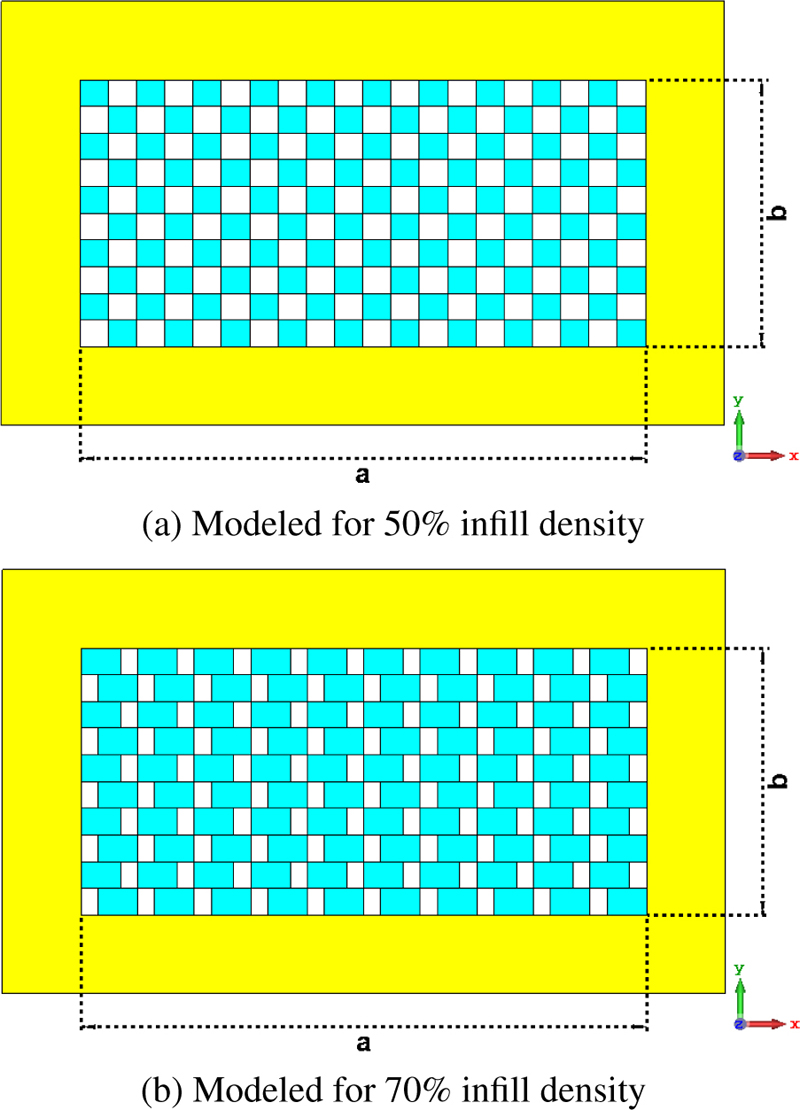
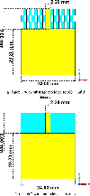
Figure 1: Cross-sectional view of modeled slabs within waveguide, each cyan block representing a unit cell.
Figure 1 presents a cross-sectional view of the dielectric slab represented by the proposed model where the printed material is represented by cyan-colored blocks within the yellow-colored waveguide. It can be seen that 70% infill exhibits higher material density compared to the 50% infill. The thickness of the slab is along the z-axis. The model was constructed such that both the larger and smaller cross-sectional inner dimensions (“a” and “b” in Figs. 1 and 2) of the waveguide were subdivided each into 10 small unit cells. The x-length of the unit cell was multiplied by the infill density factor to get the length of the printed material within the unit cell in the x direction so that the volume of the printed material in the unit cell to the volume of the unit cell represents the infill density for the dielectric slab. This approach allows for an easy method to vary the infill density by adjusting the infill percentage factor and accurately modeling infill density in terms of the volume of the printed material.
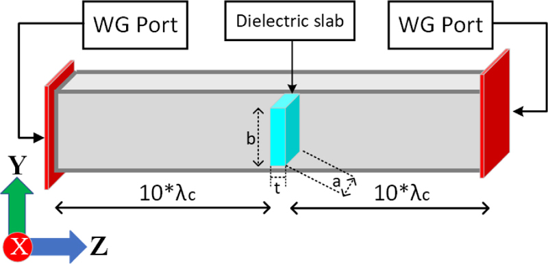
Figure 2: Model of the simulation setup depicting the waveguide and the dielectric slab.
III. SIMULATION SETUP
In this study, 7 waveguides were employed for simulations, with their dimensions listed in Table 1. These waveguides served as a basis for planned experimental assessments, based on these simulations. The frequency range encompassed by the waveguides spanned from 1 GHz (approximately 376 MHz below the WR430 cutoff frequency) to 21 GHz (within the operational range of WR42). In the simulation setup demonstrated in Fig. 2, both waveguide ends were excited by identical waveguide ports, with the dielectric slab positioned between two air-filled waveguide sections. These sections extended a length equivalent to 10 times the cutoff wavelength (based on TE mode of operation) from each side of the slab to each end of the waveguides. This configuration emulates the intended experimental setup, facilitating the attenuation of higher-order modes present at the air/material interface.
Table 1: Waveguide parameters for simulations
| Waveguide | Cross Section | |
|---|---|---|
| WR430 | 1.37 | |
| WR284 | 2.08 | |
| WR187 | 3.13 | |
| WR137 | 4.29 | |
| WR90 | 6.52 | |
| WR62 | 9.38 | |
| WR42 | 13.63 |
The various slabs used in this study share a common thickness (“t” in Fig. 2) of 27 mm, while their cross-sectional dimensions adapt to the respective waveguide dimensions. The design ensures that the inner dimensions of the waveguide fit snugly with the outer dimensions of the dielectric slabs. The dielectric slabs were oriented such that their thickness was along the z-axis as seen in Fig. 2.
The simulation results were expressed in terms of S-parameters. Since the waveguide sections were identical, the simulations yielded equivalent and and equivalent and , as expected. The results were utilized to derive the , as detailed in subsequent sections. It was observed that the values were closer to 0 dB above the cutoff frequency ranges, indicating that most of the power was transmitted between the ports, as the dielectric slabs were considered to be lossless. These values could be used to estimate the loss tangent of lossy dielectric slabs in future studies, but we did not use them for further analysis in this study, as our primary focus was investigating the real part of the permittivity.
IV. METHODOLOGY
To elucidate the methodology used to estimate the permittivity values, initially, the parameters of the simulations were defined. A specific notation was introduced for clarity and conciseness throughout the simulation process:
where “WG”corresponds to one of the specific waveguides in Table 1, “infill%”represents the infill density of the dielectric slab, “”signifies the relative permittivity value of the filament material used to fabricate the slab. For instance, WR187(70%, 2.45) represents a WR187 waveguide in which a dielectric slab with 70% infill density is inserted. The permittivity value of the filament material used to fabricate the slab was 2.45.
The algorithm proposed for determining the for a specific dielectric slab is delineated as follows:
1. Initialization: Define a dielectric slab for which the effective relative permittivity needs to be ascertained, e.g., WR187(50%,2.45).
2. Primary Simulation: Simulate the waveguide setup with the dielectric slab and record the result, e.g., :WR187(50%,2.45).
3. Record Minimum: Document the frequency at which the minimum occurs for , e.g., :WR187(50%,2.45).
4. Secondary Simulation: Simulate the same waveguide setup identical to Step 2, but with the slab at 100% infill density with set as a variable, e.g., WR187(100%,). Record the minimum as mentioned in Step 3, e.g., :WR187(100%,).
5. Iteration/Optimization: Repeat Step 4 until the absolute difference between the minimum of the Primary and Secondary simulations is less than an error threshold ().
The error threshold () was set as 0.02 GHz for this study. So, the condition that had to be satisfied for the proposed algorithm was
| (1) |
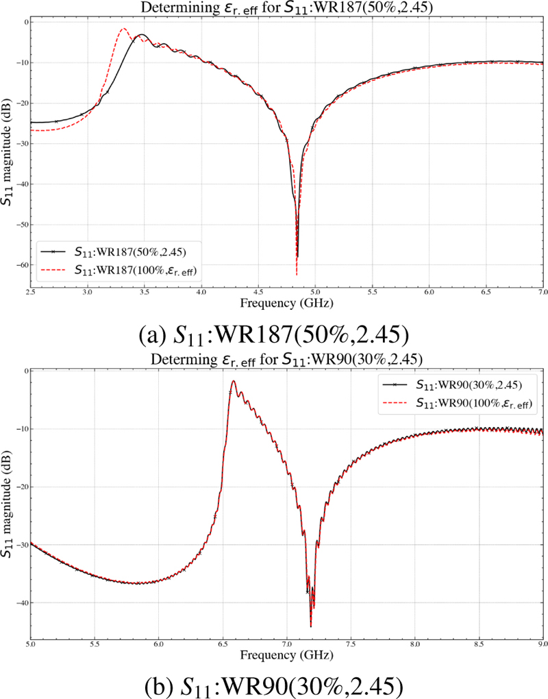
The value that satisfies expression 1 is considered to be the for WR187(50%,2.45). An example of the result obtained using this methodology is presented in Fig. 3 (a), where two data sets for WR187 namely, :WR187(50%,2.45) and :WR187(100%,) have been plotted together. The two data sets exhibit a good match, thereby indicating that the determined indeed represents the appropriate permittivity for WR187(50%,2.45) dielectric slab. Another example has been presented in Fig. 3 (b), where the permittivity for :WR90(30%,2.45) has been estimated. This simulation-based optimization methodology was employed to determine the values for each of the dielectric slabs at 30%, 50%, and 70% infilldensity.
Figure 3: Illustration of the proposed algorithm to determine .
V. RESULTS
Table 2 lists the permittivity values estimated using the proposed algorithm for each of the dielectric slabs at 30%, 50%, and 70% infill density. From Table 2, it can be seen that the is in close range of 1.4, 1.7, and 2 for 30%, 50%, and 70% infill, respectively, for all the dielectric slabs considered in this study.
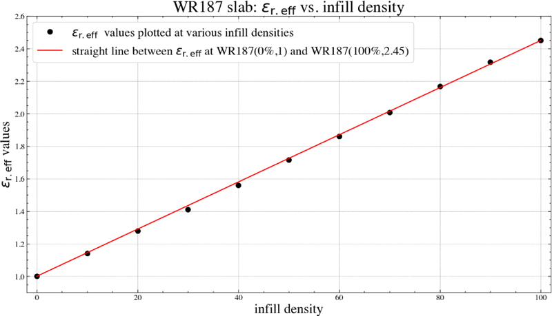
The algorithm was further employed for WR187 to estimate for all the infill densities between WR187(0%,1) and WR187(100%,2.45) in the interval of 10%. The results for the estimated (black dots) were plotted against infill density in Fig. 4. Additionally, a straight line joining the two endpoints, i.e., WR187(0%,1) and WR187(100%,2.45) was drawn (red colored line) to aid in visualizing the variation in estimated values with infill density.
VI. DISCUSSION
The estimated permittivity values presented in Table 2 elucidate that regardless of the variations in waveguide dimensions and operating frequencies, the estimated permittivity of dielectric slabs remained nearly consistent at each specific infill density. This suggests that the proposed infill model is frequency independent.
Table 2: Estimated with proposed algorithm
| Dielectric Slab | Infill | Infill | Infill |
|---|---|---|---|
| WR430 slab | 1.400 | 1.653 | 1.990 |
| WR284 slab | 1.425 | 1.715 | 2.025 |
| WR187 slab | 1.411 | 1.715 | 2.008 |
| WR137 slab | 1.422 | 1.728 | 2.000 |
| WR90 slab | 1.413 | 1.716 | 2.011 |
| WR62 slab | 1.416 | 1.722 | 2.005 |
| WR42 slab | 1.410 | 1.721 | 1.997 |
Figure 4: Linearity demonstrated between values and infill density in WR187 waveguide.
Furthermore, when the estimated values are plotted against their corresponding infill densities as presented in Fig. 4, a consistent linear relationship between values and infill density is evident. This is denoted by the fact that the estimated values (black dots) closely align with the straight red line. While this was specifically tested for WR187, it is reasonable to conclude that this relationship should hold true for the other waveguides across the entire range of simulation frequencies. This assertion is based on the consistent results generated by the proposed infill model at each of the specified infill densities outlined in Table 2. The results of the model proposed in this study are consistent with the experimental study in [1, 2, 5], where a linear correlation between and infill density was observed. This indicates that the slicer software used in those 3D printers produces the infill density appropriately similar to the model used in this study. However, if the slicer software does not add material for a particular infill density accordingly, possibly for structural integrity or other reasons, the relationship may deviate from being linear. This underscores the importance of standardizing slicer software, a point emphasized in [1].
From the results obtained, this relationship can be leveraged to estimate using the linear relation described by the equation:
| (2) |
where represents the effective relative permittivity to be determined for a lower infill%, , and are the relative permittivity of the printed material/slab at 100% infill density and air, respectively. Utilizing equation 2 for a material with = 2.45, with the fact that = 1, we computed at 30%, 50%, and 70%, resulting in 1.435, 1.725, and 2.015 respectively. These values align closely with those obtained in Table 2, demonstrating that equation 2 effectively evaluates the simulation results.
The simulations performed in this study successfully implement an infill density model that establishes a clear linear relationship between and infill density. These findings have broader implications, as they can be used to interpolate values at specific infill densities. This capability could be leveraged for design purposes, offering a valuable tool for optimizing permittivity for various applications while utilizing the same core filament material. An example to demonstrate its effectiveness has been presented in the subsequent subsection.
A. Implementing the model to optimize permittivity for the substrate of a patch antenna
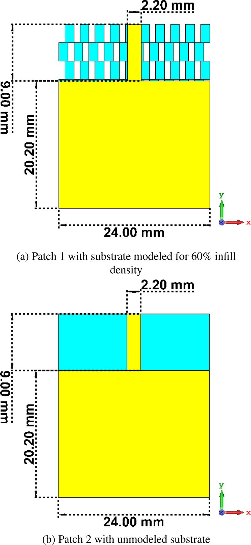
In this section, the implementation of the model in optimizing the permittivity of the substrate of a simple patch antenna is demonstrated. Two patch antennas, as illustrated in Fig. 5, were designed in CST Microwave Studio. Patch 1 substrate is modeled with 60% infill density using the volumetric model as shown in Fig. 5 (a), while Patch 2 presented in Fig. 5 (b) is without substrate modeling. Both patches share identical dimensions, as detailed in Fig. 5 with a 2 mm substrate thickness. The yellow color denotes the copper layer, while blue represents the substrate. Notably, both patches have a full ground plane on the backside, hidden in Fig. 5 for clarity of the infill model.
Figure 5: Implementing the model to optimize patch antenna.
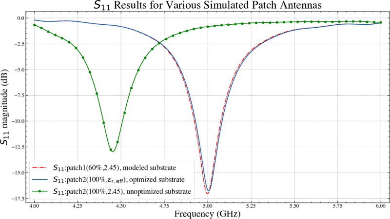
Consider a scenario where a patch antenna achieving resonance at 5 GHz necessitates a substrate with permittivity of 1.87, yet only filament with = 2.45 is available. The hypothesis questions if using that filament ( = 2.45) to design a substrate requiring = 1.87 is feasible. To investigate, patch1 (60%, 2.45) was simulated and, simultaneously, another patch patch2 (100%, ) was simulated with its substrate permittivity set as , computed using equation 2. The results of both simulations are presented in Fig. 6, indicating a close overlap between the two plots. This suggests that the substrate printed at 60% infill using a filament with = 2.45 accurately represents a permittivity of 1.87, potentially utilizing infill density as a parameter for antenna design.
Additionally, a simulation for patch2 (100%, 2.45) demonstrates the repercussions of unoptimized infill density, causing the antenna to operate at an unintended frequency range, as seen in Fig. 6. The green solid line with dots representing this result underscores the importance of utilizing appropriate infill density for the antenna substrate to achieve the desired antenna performance. Indeed, our initial experimental research of 3D printing antennas resulting in unexpected resonances due to inadequate knowledge of infill density is what led to this research in the first place.
Figure 6: Demonstrating optimized patch antenna vs. a non-optimized patch antenna.
The results obtained for patch1(60%,2.45) and patch2(100%,=1.87) in Fig. 6, suggest a simplification in modeling. It highlights the potential to bypass explicit infill density modeling for future antenna substrate simulations by simply using the from equation 2. This “100% infill”substrate with the can at a minimum, initially, negate the need for infill modeling in the design process, and that should result in quicker simulation times.
VII. CONCLUSION AND FUTURE WORK
This study contributes valuable insights into modeling infill density, elucidating a consistent linear relationship between values and infill densities. The study reveals that the increment of printed material should align linearly with increasing infill density to preserve this relationship, a crucial aspect demonstrated through the volumetric model. The derived linear equation for the model facilitates precise estimation of relative permittivity for optimizing design parameters requiring lower infill or permittivity values in specific applications. Additionally, the significance of standardizing slicer software in 3D printing processes is also highlighted to preserve this relationship.
In this study, the unit cells were designed to vary solely along the x and y directions. However, for future studies extending it to vary along the z-axis for each unit cell could allow more design flexibility and still retain the volumetric method to regulate the infill density for the printed structure as demonstrated in [6]. In upcoming research, the focus will be on experimentally validating the simulation model. This entails manufacturing dielectric slabs with different infill densities for various waveguides and subsequently comparing the effective relative permittivity obtained from simulations with empirically measured data. Additionally, attention will be given to investigating an analytical approach to develop a theoretical model on the effective relative permittivity for the lower infill densities. These studies hold substantial promise for designing and manufacturing customized dielectric substrates with tailored dielectric properties, further broadening the scope of applications of 3D printing technology across various domains.
ACKNOWLEDGMENT
We are thankful to the Raytheon Co. and the National Science Foundation as this work was supported in part by the NSF Industry-University Cooperative Research Centers (I-UCRC) under Grant 1822104. We acknowledge the use of SciencePlots [7] and Matplotlib for creating the plots in this paper.
REFERENCES
[1] B. Kattel, W. E. Hutchcraft, and R. K. Gordon, “Exploring infill patterns on varying infill densities on dielectric properties of 3D printed slabs,” 2023 Antenna Measurement Techniques Association Symposium (AMTA), pp. 1-5, 2023.
[2] B. T. Malik, V. Doychinov, S. A. R. Zaidi, I. D. Robertson, and N. Somjit, “Antenna gain enhancement by using low-infill 3D-printed dielectric lens antennas,” IEEE Access, vol. 7, pp. 102467-102476, 2019.
[3] B. Kattel, W. E. Hutchcraft, and R. K. Gordon, “3D printed patch antennas with varying infill densities,” 2023 Antenna Measurement Techniques Association Symposium (AMTA), pp. 1-5, 2023.
[4] B. Kattel, “Evaluation of wireless router antennas and 3D-printed simulated antenna designs,” Electronic Theses and Dissertations, vol. 1769, 2019.
[5] H. Hu, S. Sinha, N. Meisel, and S. G. Bilén, “Permittivity of 3D-printed nylon substrates with different infill patterns and densities for design of microwave components,” Designs, vol. 4, no. 3, 2020.
[6] B. F. LaRocca and M. S. Mirotznik, “Modeling the performance impact of cubic macro cells used in additively manufactured luneburg lenses,” Applied Computational Electromagnetics Society (ACES) Journal, vol. 37, no. 10, pp. 1077-1088, 2023.
[7] J. D. Garrett, “garrettj403/SciencePlots,” Zenodo, Sep. 2021.
BIOGRAPHIES

Bibek Kattel is a doctoral candidate in the Department of Electrical and Computer Engineering at the University of Mississippi, Oxford, MS. He earned his M.Sc. in Electrical Engineering with an emphasis in Electromagnetics from the same university in 2019.
His current research focuses on the design and fabrication of 3D printed antennas, RF and antenna measurements, and exploring novel materials for 3D printing applications. In addition to research, he has a passion for teaching and has taught an electronics course at the University of Mississippi in Fall 2023. He is a member of Phi Kappa Phi.

W. Elliott Hutchcraft was born in Lexington, Kentucky on April 29, 1973. He earned his B.S. in electrical engineering at the University of Mississippi, Oxford, MS in 1996, his M.S. in electrical engineering at the University of Mississippi, Oxford, MS in 1998, and his Ph.D. in electrical engineering at the University of Mississippi, Oxford, MS in 2003.
He is an Associate Professor in the Department of Electrical and Computer Engineering at the University of Mississippi in Oxford, Mississippi. Dr. Hutchcraft is a member of Eta Kappa Nu, IEEE, Tau Beta Pi, and Phi Kappa Phi.

Richard K. Gordon is from Birmingham, Alabama. He earned his B.S. in physics at Birmingham-Southern College, Birmingham, AL in 1983, his M.S. in applied mathematics at the University of Illinois, Urbana, IL in 1986, and his Ph.D. in electrical engineering at the University of Illinois, Urbana, IL in 1990.
He is an Associate Professor in the Department of Electrical and Computer Engineering at the University of Mississippi in Oxford, Mississippi. Dr. Gordon is a member of Eta Kappa Nu, Phi Beta Kappa, and TauBeta Pi.
ACES JOURNAL, Vol. 38, No. 12, 981–986
doi: 10.13052/2023.ACES.J.381208
© 2023 River Publishers
