A Band Stop to Band Pass Filter Transformation Utilizing 3-D Printing Technique for C-band Applications
Wael A. E. Ali1, Ahmed A. Ibrahim2, and Ashraf E. Ahmed3
1Department of Electronics & Communications Engineering, College of Engineering and Technology, Arab Academy for Science, Technology and Maritime Transport (AASTMT), Alexandria, Egypt
wael.ali@aast.edu
2Electronic Engineering Department, Minia University, El-Minia, Egypt
ahmedabdel_monem@mu.edu.eg
3Electronics & Comm. Engineering Department, College of Engineering, Higher Institute of Engineering and Technology, King Marriott, Alexandria, Egypt
aeltyib_ahmd@yahoo.com
Submitted On: July 26, 2022; Accepted On: December 20, 2022
ABSTRACT
In this paper, a band-pass filter (BPF) based on split-ring resonator (SRR) using a 3-D printing technique for C-band applications is introduced. The proposed filter is designed to operate at a frequency of 3.9 GHz. An innovative technique for printing the substrate with a size of 24 24 1.1 mmusing PLA dielectric material is implemented. The copper sheet with a thickness of 0.1 mm is printed on the upper and lower faces of the substrate. First, the SRR band stop filter (BSF) is introduced then two L-Stubs are inserted to implement an additional band stop region, and this rejoin is adjusted to obtain a band-pass region between the two stopbands. The BPF is operated at a 3-dB bandwidth extended from 3.5 GHz to 4.3 GHz with an S level of 0.2 dB for the simulated results while it achieves a 3-dB bandwidth within 3.6 GHz to 4.2 GHz (15.3 %) with an S level of 1.8 dB for the measured results.
Index Terms: 3-D printing, bandpass filter, C-band applications, PLA.
1 INTRODUCTION
Filters play a very important role in many RF microwave applications. They are commonly utilized in transceiver circuits to isolate or merge various frequencies. A band-pass filter allows components to pass in a specific frequency band, known as the passband while blocking other components of frequencies that are higher than or lower than this band [1, 2]. Bandpass filters are commonly used in wireless transmission and reception. The main purpose of the filter is to pass an output signal with a certain range of frequencies allocated for transmission to avoid interference with the neighboring [3, 4]. Several studies are conducted to achieve a bandpass behavior that fulfills modern technological market needs such as compact size, sharp roll-off rate, wide stopband, and low passband insertion loss [5–9]. Various techniques are carried out to achieve the required bandpass behavior as in [10–17]. In [10], the defected ground structure is used to obtain a wide band stop behavior while passing all frequencies in the range of 2.4-14.3 GHz. The stepped impedance resonator (SIR) is one of the most commonly used techniques to provide a bandpass behavior and it succeeded to achieve a triple band (1.85 GHz, 2.575 GHz, and 3.05 GHz) with skew-symmetric (0-degree) tapped-feed structure as in [11]. The open-loop resonator (OLR) technique was carried out in [12] for dual passbands (WLAN and WiMAX). Another technique substrate integrated wave (SIW) was used in [13] to achieve a band-pass response (15.6–32.1 GHz) in the RF and millimetric wave frequency range with an enhanced insertion loss in the passband ( 0.8 dB). To obtain a millimeter band-pass response, a split ring resonator (SRR) was used [14], and the achieved performance was quite enough to make the suggested filter a good candidate for 5G networks.
Nowadays, 3-D printing, or additive manufacturing (AM), is the building block of a three-dimensional object from a digital 3-D model. The entire 3D printing technology can be divided into 3 steps 1 3D design, 2 slicing, 3 3D printing [15]. 3D printing techniques are used recently in designing microwave components such as filters and antennas. It can be used to construct antenna models for multiband applications as in [16–19]. Additionally, there are various designs of microwave filters based on 3D printing in the RF frequency range [20–21], and the implemented BPF in [22] was operated in the E-band (60-90 GHz) of the millimetric wave frequency range, but with inconsistent simulation and experimental results due to fabrication tolerance.
2 SRR BSF
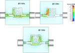
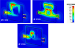
The 2-D structure of the SRR BSF is illustrated in Fig. 1. The BSF has a /2 open-loop transmission line and the SRR is fed by a 50 microstrip line connected with SMA connectors. The PLA substrate material with a dielectric constant of 3.1, loss tangent of 0.001, and height of 1.1 mm is utilized. The detailed dimensions of the filter parameter are depicted in Fig. 1 (a) and listed in the figure caption. The simulated (CST & HFSS) outcomes of the BSF are illustrated in Fig. 2. The suggested BSF is operating at 5 GHz with 2.7 GHz 3-dB bandwidth from 3.7 GHz to 6.4 GHz) and the achieved return loss over the entire stopband is approximately 0.2 dB. To verify the achieved results in Fig. 2 the electric field distribution is simulated at different frequencies outside (3 and 7 GHz) and inside the stopband (5 GHz) as shown in Fig. 3. It is clear that at 3 GHz, the electric field is conducted to port 2 through the open-ended loop as shown in Fig. 3 (a) and the same behavior is noticed when the filter is excited at 7 GHz but the major concentration of field was through the aligned arm of the resonator with the two feedlines as shown in Fig. 3 (c). However, at 5 GHz as shown in Fig. 3 (b), the electric field couldn’t pass to port 2 and is concentrated on port 1 and the left part of SRR confirming the capability of the suggested filter to behave as a BSF in the desired band. Furthermore, the current distribution of the suggested filter is demonstrated in Fig. 4 and the current distribution is carried out at the same three frequencies which were used in the field distribution confirming the ability of the suggested filter to pass all frequencies except the desired band from 3.7 to 6.4 GHz.
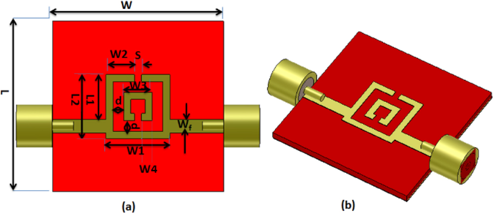
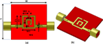
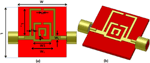
Figure 1: The configuration of SRR BSF. (a) 2-D configuration with W = L = 24 mm, W1 = 9 mm, W = 1.95 mm, d = 1.5 mm, S = 1mm, W2 = 4 mm, L1 = 6.3 mm, L2 = 9 mm, W3 = 4 mm, and W4 = 1.5 mm. (b) 3-D configuration.
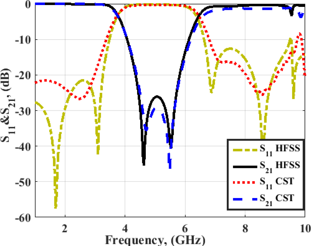
Figure 2: The simulated SRR BSF S-parameters results.
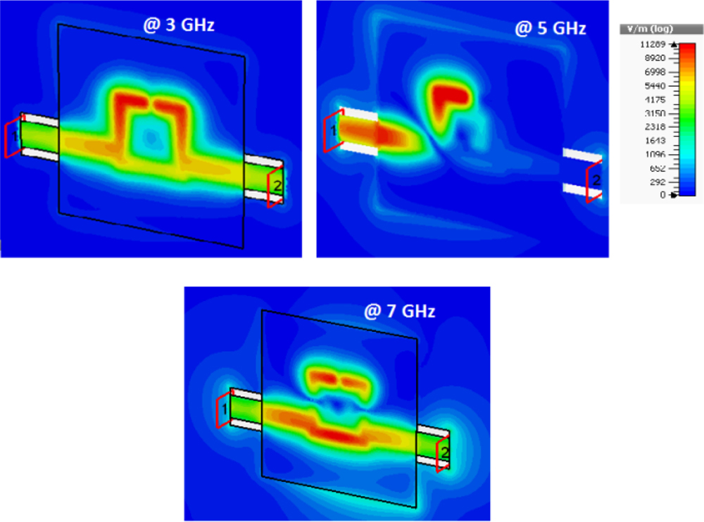
Figure 3: The simulated distributions of electric field results of SRR BSF at z=0.6 mm (inside substrate).
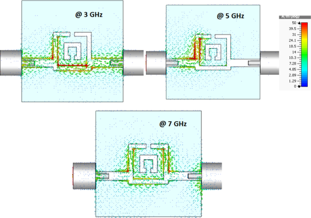
Figure 4: The current distribution’s simulated results of SRR BSF.
3 PROPOSED SRR BPF/BSF
To produce the dual-band operation of the SRR-BSF, an additional resonator is introduced in Fig. 5 with dimensions L and W. It is worth noting that the dimensions of the additional resonator are larger than the fundamental one, so the achieved rejection band will be in the lower frequency range. Consequently, it is evident from Fig. 6 of the achieved simulated results of insertion and return loss using HFSS and CST programs that the suggested filter has two operating stopbands, the first one covers the range from 2.1 to 3.4 GHz with a deeper insertion loss of 47 dB at 3 GHz, and the second band covers the old frequency range with a reduction of 0.4 GHz (4.4 – 6.4 GHz) and this is due to the coupling with the additional SRR. Furthermore, a new BPF behavior is accomplished in the frequency range (3.5 – 4.3 GHz) with an insertion loss of level 0.2 dB confirming the readability of the suggested BPF to be embedded in different applications that cover the achieved frequency band. There is a discrepancy between HFSS and CST results, especially at the extremely lower and higher frequencies of the achieved rejection bands and this may be due to the different meshing operations of both programs.
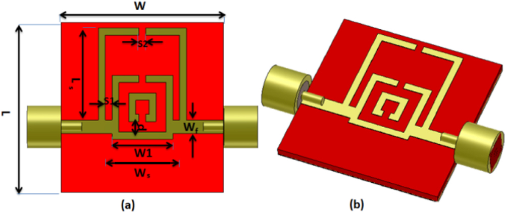
Figure 5: The configuration of the proposed SRR BPF/BSF (a) 2-D configuration with W= L=24 mm, W1= 9 mm, W = 1.95 mm, d= 1.5 mm, S1=1 mm, S2= 1 mm, L= 13 mm, W = 10 mm (b) 3-D configuration.
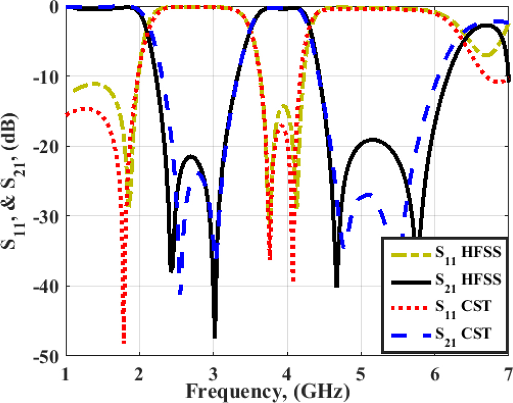
Figure 6: S-parameters simulated results of SRR BPF/BSF.
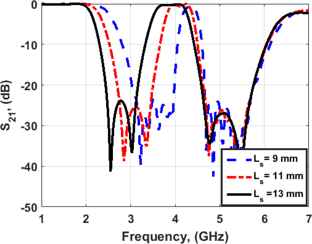
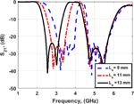
Figure 7: The S simulated results of SRR BPF/BSF at different values (Ls).
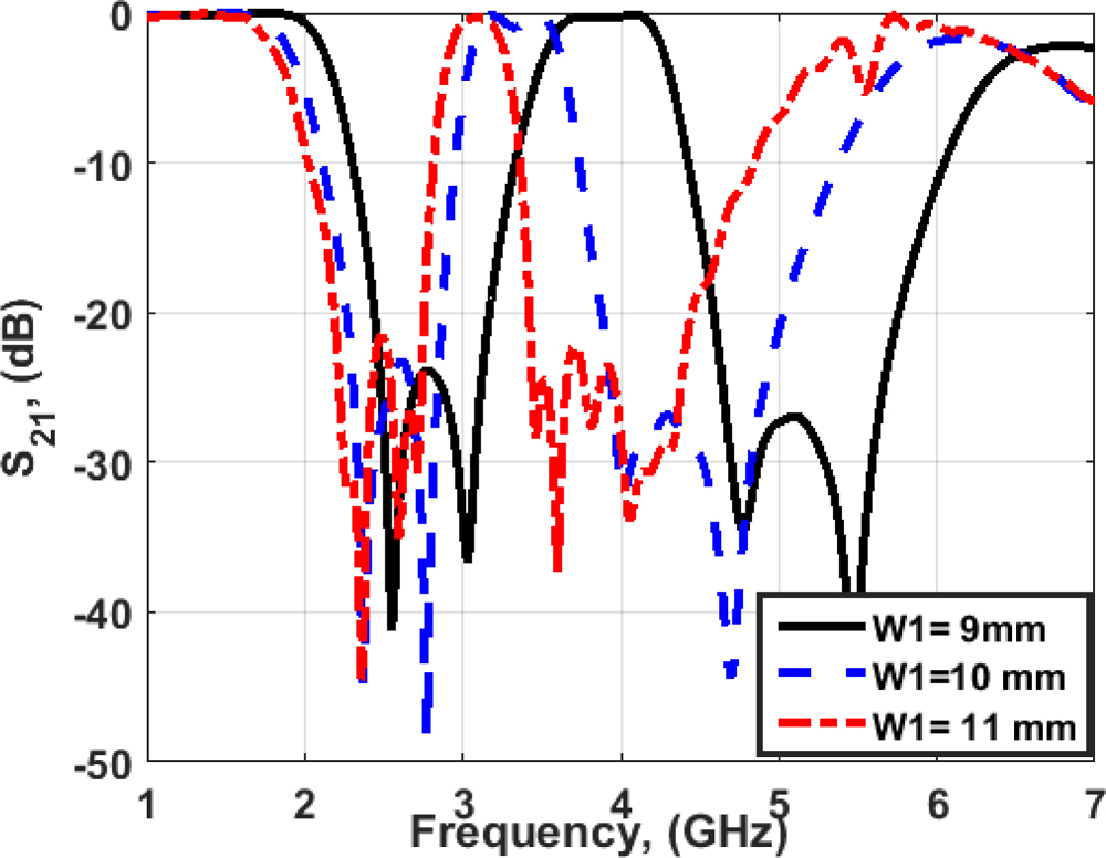
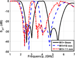
Figure 8: The S simulated results of SRR BPF/BSF at different values (W1) of the SRR cell.
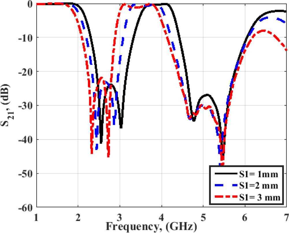
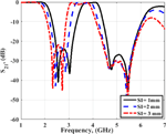
Figure 9: The S simulated results of SRR BPF/BSF for different values of S1.
The parametric study is carried out to illustrate the effect of the SRR length (Ls), its width (W1), and the spacing between inner and outer SRRs (S1) on the filter performance. The effect of changing the length of Ls on the behavior of the proposed filter is presented in Fig. 7 and it is obvious that the length change has a significant effect on the lower band since the operating frequency is translated to the lower range by increasing Ls, also it has a minor effect on the achieved upper-frequency band. Another parameter is changed to investigate its effectiveness which is the width “W1”. It can be observed from Fig. 8 that both stopbands are translated to a lower range by increasing W1 and the level of translation in the higher band is greater than that of the lower band since the shift in the upper band is about 0.8 GHz and the lower band 0.4 GHz when increasing W1 to 10 mm. Additionally, when increasing W1 to 11 mm, the upper band is shifted down by 0.6 GHz and the lower band by 0.1 GHz. Consequently, the parameter W1 has a great influence, especially for the upper stopband and it also deteriorates the insertion loss performance when it is increased. It is very obvious in the passband since it is not only decreasing the insertion loss level but also the achieved bandwidth as demonstrated in Fig. 8. The parametric study of the last investigated parameter “S1” is clarified in Fig. 9. The spacing between the SRR and the L-stubs has a significant effect on the lower rejection band since the frequency is shifted down by about 0.2 GHz per increase of 1 mm for S1. Hence, the achieved passband is translated to a lower frequency range with an increased passband bandwidth but with the degraded performance of insertion loss.
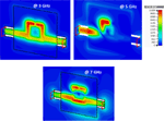
The surface current distribution of the suggested filter is investigated to verify the BPF performance at three resonance frequencies (3, 4, and 5 GHz). As can be observed in Fig. 10, the current is uniformly distributed from port 1 to port 2 at 4 GHz, while it is blocked at the left side of the L-stubs when it is simulated at 3 GHz and the left side of the primary SRR when it is simulated at 5 GHz.
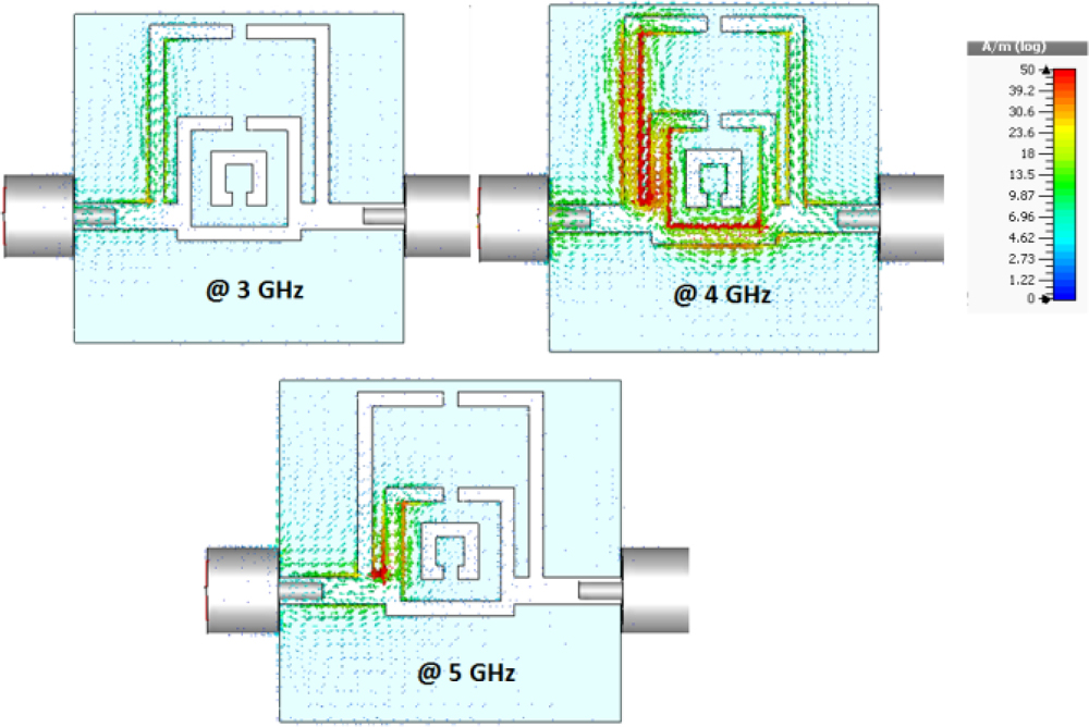
Figure 10: The current distribution’s simulated results of SRR BPF/BSF.
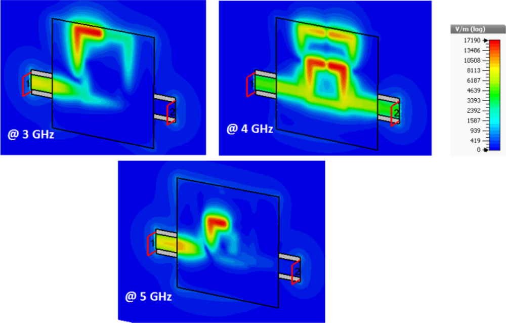
Figure 11: The electric field distribution’s simulated results of SRR BPF/BSF at z=0.6 mm.
The same performance is achieved when the electric field is investigated as in Fig. 11 confirming the ability of the suggested BPF to transfer all signals in the desired frequency band (3.5-4.3 GHz) only while rejecting all other frequencies.
4 EXPERIMENTAL OUTCOMES
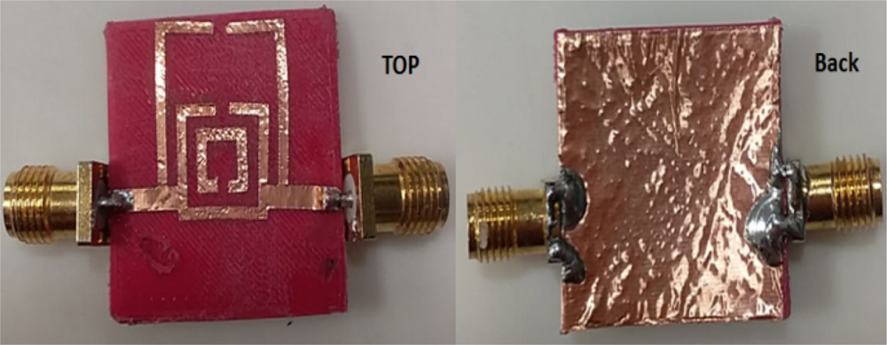
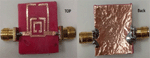
Figure 12: The fabricated photo of the proposed SRR BPF/BSF.

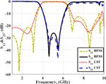
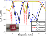
Figure 13: The S-parameters simulated and measured results of SRR BPF/BSF.
Table 1: Comparison between proposed work and reported filters
| Ref. | Response | f (GHz) |
S (dB) |
Size () | /h (mm) |
| FBW (%) | |||||
| [8] | Single-BPF | 5.3 | 1.5 | 0.58 0.65 | 3.38/0.813 |
| 8.68 | |||||
| [9] | Triple-BPF | 6.5/7.35 /8.15 |
1.74/1.82 /1.96 |
2.2 0.61 | 2.2/0.787 |
| 2.31/2.04 /2.45 |
|||||
| [10] | UWB-BPF | 8.35 | 1.5 | 1.28 0.36 | 4.4/1.6 |
| 143 | |||||
| [23] | Triple-BPF | 2.5/3.4 /4.9 |
- | 0.49 0.37 | 2.2/0.787 |
| 12/21/25 | |||||
| [24] | Triple-BPF | 1.75/2.55 /3.55 |
0.55/1.36 /1.37 |
0.32 0.12 | 2.2/1.575 |
| 21.2/4.7 /8.4 |
|||||
| This work | Single-BPF | 3.9 | 1.8 | 0.55 0.55 | 3.1/1.1 |
| 15.3 |
The proposed SRR-based BPF/BSF is fabricated using copper tape of the thickness of 0.1 mm and then implemented on a layer of 3-D printed PLA substrate with 3.1 dielectric constant and 2 mm thickness. Two 50-ohm SMA connectors are connected to the suggested filter through 50-ohm transmission lines as depicted in Fig. 12. The proposed filter is tested to verify its behavior using R&S ZVB 20 vector network analyzer (VNA). The simulated and measured results of return and insertion losses are presented in Fig. 13. The BPF is operated at 3-dB bandwidth extended from 3.5 GHz to 4.3 GHz with an S level of 0.2 dB for the simulated results, while it achieves 3-dB bandwidth within 3.6 GHz to 4.2 GHz (15.3 %) with an S level of 1.8 dB for the measured results. Good consistency between the simulated and the measured results can be noticed with a slight reduction of the achieved band and this may be due to the non-conformal stacking of the copper tape on the PLA surface and the misalignments of copper tape sections. A comparison with the recently reported work is illustrated in Table 1.
5 CONCLUSION
A compact 3-D printing BPF has been proposed. The filter has been printed on a PLA substrate. The entire size of the final filter substrate was 24 24 1.1 mm. The BPF has been operated at a 3-dB bandwidth extended from 3.4 GHz to 4.3 GHz with an S level of 0.2 dB for the simulated results while it achieves a 3-dB bandwidth within 3.6 GHz to 4.2 GHz (15.3 %) with an S level of 1.8 dB for the measured results. These outcomes enable the filter can be used in C-band applications.
REFERENCES
[1] L. Zhou, Y. Z. Yin, W. Hu, and X. Yang, “Compact bandpass filter with sharp out-of-band rejection and its application,” Applied Computational Electromagnetics Society (ACES) Journal, vol. 32, no. 3, pp. 249-255, 2017.
[2] A. Rajput, K. Patel, and A. Birwal, “Compact microstrip low pass filter design using U-shaped folded high-impedance line,” Microwave and Optical Technology Letters, vol. 60, no. 7, pp. 1812-1815, 2018.
[3] A. A. Ibrahim, M. A. Abdalla, and W. A. E. Ali, “Small size and wide-band band pass filter with DGS/CRLH structures,” Applied Computational Electromagnetics Society (ACES) Journal, vol. 34, no. 5, pp. 777-783, 2019.
[4] Z. Zhu, L. Cao, and C. Wei, “Novel compact microstrip dual-mode filters with two controllable transmission zeros,” Applied Computational Electromagnetics Society Journal (ACES), vol. 33, no.1, pp. 43-48, 2018.
[5] A. Sami, M. Rahman, H. Ahmad, and S. Bashir, “Design strategy for compact bandpass filters using meander line resonators,” Applied Computational Electromagnetics Society (ACES) Journal, vol. 35, no. 1, pp. 44-50, 2020.
[6] A. A. Ibrahim, H. A. Mohamed, and W. A. E. Ali, “Tunable dual/triple band-pass filter based on stub-loaded resonators for wireless applications,” Journal of Instrumentation, vol. 12, pp. 1-12, 2017.
[7] A. A. Ibrahim, W. A. E. Ali, and M. A. Abdelghany, “Design of dual-band dual-mode band-pass filter utilizing 0 feed structure and lumped capacitors for WLAN/WiMAX applications,” Electronics, vol. 9, no. 10, pp. 1697, 2021.
[8] A. Boutejdar, A. A. Ibrahim, and W. A. E. Ali, “Design of compact size and tunable band pass filter for WLAN applications,” Electronics Letters, vol. 52, no. 24, pp. 1996-1997, 2016.
[9] Z. Yang, B. You, and G. Luo. “Dual/tri-band bandpass filter using multimode rectangular SIW cavity,” Microwave and Optical Technology Letters, vol. 62, no. 3, pp. 1098-1102, 2020.
[10] K. A. Ansal, D. S. Jose, A. S. Kumar, and T. Shanmugantham, “A band pass coupled line filter with DGS for ultra-wide band application,” Procedia Computer Science, vol. 171, pp. 561-567, 2020.
[11] J. Chen, J. Zhong, J. Shen, N. Gao, and A. Zhang, “Design of compact tri-band filter based on sir-loaded resonator with 0 tapped-feed structure,” Frequenz, vol. 69, no. 9-10, pp. 389-392, 2015.
[12] A. A. Ibrahim, M. A. Abdalla, and W. A. E. Ali, “Dual band pass filter with sharp transmission zeros for wireless applications,” Journal of Instrumentation, vol. 13, no. 6, P06020, 2018.
[13] L. Zhao, Y. Li, Z. M. Chen, X.H. Liang, J. Wang, X. Shen, and Q. Zhang, “A band-pass filter based on half-mode substrate integrated waveguide and spoof surface plasmon polaritons,” Scientific Reports, vol. 9, no. 1, pp.1-8, 2019.
[14] M. Amzi, S. D. Bennani, J. Zbitou, and A. Belmajdoub, “Design of compact bandpass filter based on SRR and CSRR for 5G applications,” International Conference on Electronic Engineering and Renewable Energy, Springer, Singapore, pp. 175-181, 2020.
[15] G. Carranza, U. Robles, C. L. Valle, J. J. Gutierrez, and R. C. Rumpf, “Design and hybrid additive manufacturing of 3D/volumetric electrical circuits,” IEEE Trans. on Components, Packaging, and Manufacturing Technology, vol. 9, no. 6, pp. 1176-1183, 2019.
[16] A. E. Ahmed, W. A. E. Ali, A. Chowdhury, and S. Das, “A 3-D printed trapezoidal antenna for X-band wireless communications applications,” Futuristic Communication and Network Technologies, Springer, Singapore, pp. 949-956, 2022.
[17] A. E. Ahmed and W. A. E. Ali, “Analysis and design of 3-D printed fractal triangular antenna for wireless communications applications.” International Conference on Electrical, Communication, and Computer Engineering (ICECCE), pp. 1-5, 2020.
[18] A. E. Ahmed, W. A. E. Ali, and S. Das, “Quintuple band circular monopole antenna with innovative3-D printed PLA substrate for wireless applications,” Frequenz, vol. 76, no. 3-4, pp. 199-207, 2022.
[19] A. E. Ahmed, W. A. E. Ali, and S. Das, “A 3D printed 2x2 circular planar antenna array for wireless communications applications,” Journal of Nano-and Electronic Physics, vol. 13, no. 3, pp. 03028-1-03028-4, 2021.
[20] I. O. Saracho-Pantoja, J. R. Montejo-Garai, J. A. Ruiz-Cruz, and J. M. Rebollar, “Additive manufacturing of 3D printed microwave passive components,” Emerging Microwave Technologies in Industrial, Agricultural, Medical and Food Processing, p. 93, 2018.
[21] U. Robles, E. Bustamante, P. Darshni, and R. C. Rumpf, “High-frequency filters manufactured using hybrid 3D printing method,” Progress In Electromagnetics Research M, vol. 84, pp. 147-155, 2019.
[22] B. Zhang and H. Zirath, “3D printed iris bandpass filters for millimetre-wave applications,” Electronics Letters, vol. 51, no. 22, pp. 1791-1793, 2015.
[23] T. A. Sheikh, J. Borah, and S. Roy. “Design of compact bandpass filter for WiMAX and UWB application using asymmetric SIRs and DGS,” Radioelectronics and Communications Systems, vol. 59, no. 6, pp. 269-273, 2016.
[24] T. Firmansyah, M. Alaydrus, Y. Wahyu, E. T. Rahardjo, and G. Wibisono, “A highly independent multiband bandpass filter using a multi-coupled line Stub-SIR With folding structure,” IEEE Access, vol. 8, pp. 83009-83026, 2020.
BIOGRAPHIES
Wael A. E. Ali was born in 1982. He received his B.Sc. and M.Sc. in Electronics and Communications Engineering from the Arab Academy for Science, Technology and Maritime Transport (AASTMT), Alexandria, Egypt in 2004 & 2007, respectively. He received his Ph.D. in Electronics and Communications Engineering from Alexandria University, Alexandria, Egypt in 2012. He is now a Professor of Electronics and Communications Engineering, as well as the Head of the Quality Assurance unit in the College of Engineering and Technology.

Ahmed A. Ibrahim was born in 1986. He received his B.Sc. degree, M.Sc., and Ph.D. in Electrical Engineering from the Electronic and Communication Engineering Department, Minia University, Elminia, Egypt in 2007, 2011, and 2014 respectively. He is now an Associated Professor at the Electrical Engineering Department in the Faculty of Engineering, Minia University.

Ashraf E. Ahmed is currently a lecturer at the Electronics and Communications Engineering Department, Higher Engineering and Technology, King Marriott Academy (KMA), Alexandria, Egypt. He received his B.Sc. and M.Sc. degrees in Electronics and Communication Engineering from the Faculty of Engineering, Alexandria University, Egypt.
ACES JOURNAL, Vol. 37, No. 11, 1146–1152
doi: 10.13052/2022.ACES.J.371105
© 2022 River Publishers