CMOS High Swing and Q Boosted Dual Core Voltage Controlled Oscillator for 5G New Radio Application
Pravinah Shasidharan, Jagadheswaran Rajendran, Selvakumar Mariappan, Narendra Kumar, and Masuri Othman
1Collaborative Microelectronic Design Excellence Center (CEDEC)
Universiti Sains Malaysia, Sains @USM, Bayan Lepas (Penang), 11900, Malaysia
pravinah.shasidharan@student.usm.my, jaga.rajendran@usm.my, selva_kumar@usm.my
2Department of Electrical Engineering, Faculty of Engineering
University of Malaya, Kuala Lumpur, 50603 Malaysia
narendra.k@um.edu.my
3Institute of Microengineering and Nanoelectronics
National University of Malaysia
Bangi, 43600, Malaysia
masuri@ukm.edu.my
Submitted On: August 19, 2022; Accepted On: July 10, 2023
ABSTRACT
This paper describes a low power, low phase noise CMOS voltage controlled oscillator (VCO) with a cascoded cross-coupled pair (XCP) configuration for high data rate 5G New Radio (5G-NR) applications. The core consists of a primary auxiliary VCO built as a negative conductance circuit to improve phase noise and a secondary core with a cascoded formation to increase output voltage swing. A switched varactor array (SVA) wideband tuner is integrated for a wide bandwidth application in a low power implementation. The dual-core VCO was designed in CMOS 130 nm technology and occupies only 1.05 mm of space. With a supply voltage of 1.2 V, the VCO achieved a tuning range of 32.43% from 3.45 GHz to 4.47 GHz. At 3.96 GHz carrier center frequency with 1 MHz offset, the total power consumption is 0.7 mW with a corresponding phase noise (PN) of 121.25 dBc/Hz and a Figure of Merit (FoM) of 193.25 dBc/Hz. The results are validated using Cadence Spectra RF simulations.
Index Terms: cascode, CMOS, cross-coupled pair, 5G, New Radio, Q enhancement, switched varactor array (SVA), Voltage Controlled Oscillator.
I. INTRODUCTION
The 5th generation radio system is entirely dependent on fast data rates and low latency. This raises the bar for improved front-end system performance, particularly in the transceiver system. In general, any transceiver system requires a stable oscillator that provides low noise performance while also consuming little power. The power consumption should be low enough to avoid exorbitant maintenance costs, such as frequent battery replacement and higher manufacturing costs. It is still a challenge today, as many oscillators with low power consumption have difficulty achieving low phase noise and wide bandwidth applications. Wideband applications have made extensive use of switched active cores [1–2]. The switched inductor array, which greatly increased the chip’s area is the most widely used for bandwidth extension. Many digital switches experience a variety of issues, which contribute to the complexity of tuning voltages as well as the risk of tuning range gaps [3–5]. However, a novel varactor [6] has been proposed to broaden the tuning range using a single varactor without the need for digital control signal tuning achieving a tuning range of 40.3%. Some work encounters a disadvantage in improving phase noise at the expense of increased die area and a low quality factor (Q). Work [7] implements a Q enhancement and filtering technique without affecting the tank circuit’s inductor component. To reduce the noise, a narrow band filter with a capacitor is placed on the current source [8].
Another method is to bias the capacitor placed between the gate and drain of the tail current source at twice the oscillation frequency of the resonant tank in order to suppress the flicker noise cause by the active devices. The transistor has been cleverly designed to be cycled between strong inversion and accumulation mode operation to reduce flicker noise contribution [9]. Aside from that, another technique has been implemented that involves operating the transistor in the weak inversion (WI) region to achieve low power performance at the expense of poor process, voltage and temperature (PVT) variation [10]. The current reuse technique has been proposed to reduce power consumption, but the drawback is that it causes some asymmetrical output in the amplitude of the oscillation swing, which triggers flicker noise up-conversion and degrades the performance of the VCO’s phase noise [11–15]. Another approach, on the other hand, has been taken to properly model the varactor noise in order to reduce an avalanche phenomenon that can cause controllable phase noise [16].
However, extreme action is required at the varactor device to avoid device degradation caused by enormous high breakdown when VCO output swing is large. As a low phase noise VCO, being unaware of the effect of varactor breakdown noise may result in difficult simulation results. In this work a dual-core VCO is implemented, with the primary core acting as a Q enhancement circuit without affecting the structure of the tank inductor and the secondary core acting as a high swing trigger. Both cores have an adequate biasing scheme and have attained a suitable biasing point for better phase noise under low power consumption. The remainder of the paper is structured as follows. The principle of operation and its design concept are explained in detail in section II. Section III presents the performance reliability results and section IV concludes.
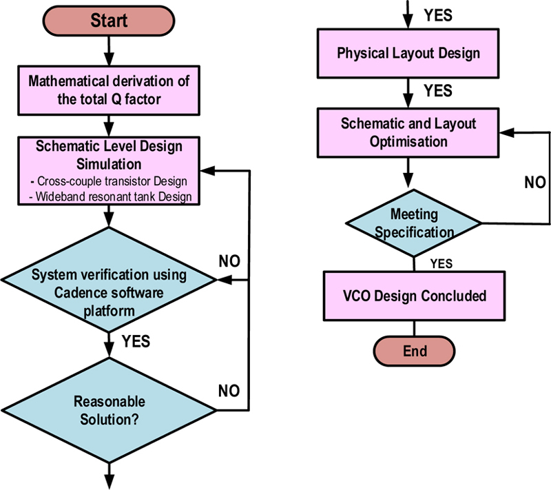
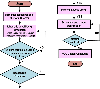
Figure 1: Flow chart of the design flow for the proposed VCO
II. PRINCIPLE OF OPERATION AND DESIGN CONCEPT
A. Dual core VCO circuit design
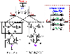
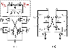
Figure 1 illustrates the design flow chart that describes the top-down approach which starts with mathematical analysis on determining the Q factor for the proposed circuit. Predetermined simulations and system verification were performed under the Cadence environment. Here, the schematic to the layout process flow is achieved with further optimization until the proposed specifications are met. With this, the proposed wideband, low power, dual core VCO is shown in Fig. 2. The architecture of the VCO consists of two sets of cores: the primary auxiliary core and the secondary core. The auxiliary structure comprises of the cross-coupled pairs N and N stacked on top of the cross-coupled pairs, N and N, which function as a gain booster and contributes to an increase of the Q factor via the bias voltage, V. The secondary core, consisting of a cascode pseudo differential pair comprised of N to N, is gate driven using a single biasing voltage, V. The transistors are sized symmetrically and merged with the primary core in order to improve the VCO’s swing and start-up. The resistors and capacitor, RC and RC, are dynamically biased to permit a wider output swing at the nodes of the V and V, which is sufficient to meet an oscillator’s start-up condition. The VCO is equipped with a wideband tuner consisting of an inductor, L and a switched varactor array, SVA which are arranged in parallel and consist of the multiple tuner voltage V through V. For wideband operation, the capacitor values of the varactor capacitors are sized differently.
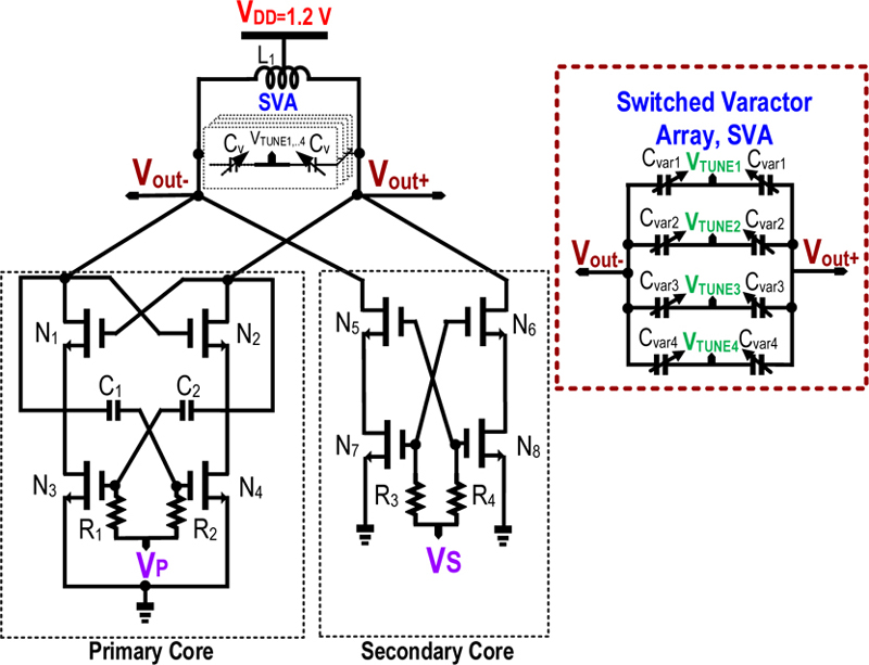
Figure 2: Proposed LC-VCO with dual core VCO.
B. Theory of operation of primary core
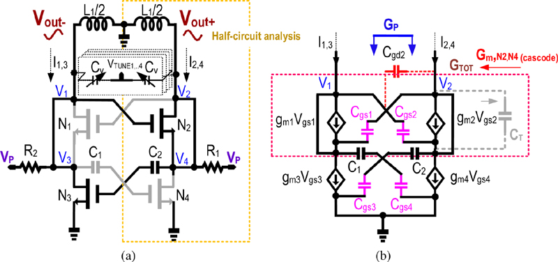
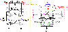
Figure 3: Primary core (a) circuit and (b) small signal equivalent model.
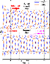
As observed in Fig. 3 which shows the circuit operation of the primary core where Fig. 3 (a) shows the detail representation of the primary core of a cross couple structure (XCP) whereas Fig. 3 (b) shows a model of the cross-couple structure’s small signal equivalent. Two feedback-biased cross-coupled devices which linked to the feedback-biased voltage, V provide the drain current flows of I and I respectively. When oscillation begins, the differential oscillator signal, V and V determine the conduction mode of the stacked transistor N-N. Figure 4 shows the drain current of transistors N and N become zero when the local oscillator (LO) switches to . The conduction period of the LO signal is shown in Fig. 5.
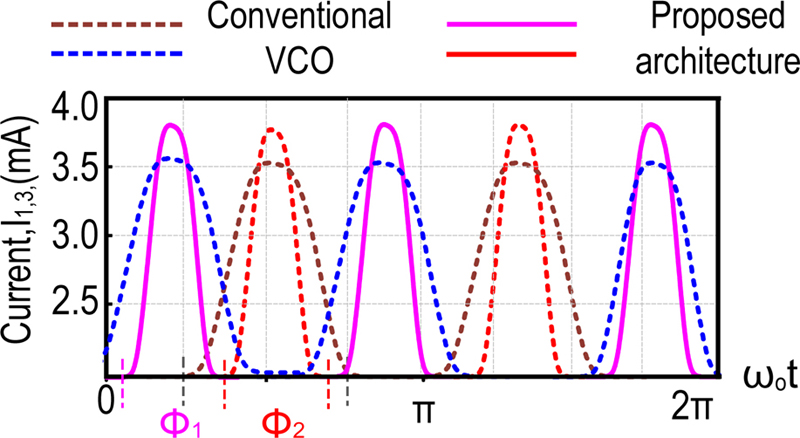
Figure 4: Simulated MOS current waveform for the dual core conduction.
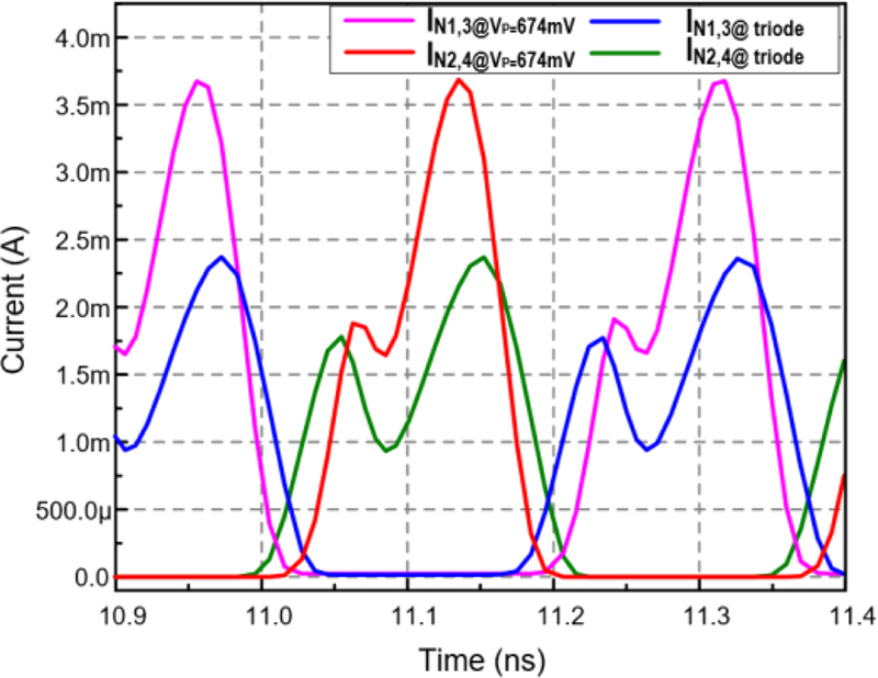
Figure 5: Simulated drain current waveform for the dual core VCO.
Hence, when the LO switches during the interval, N and N are both fully on while N and N are both fully off. The current flowing to the output has been inverted since the pair of transistors have been switched alternately. In this repeated process, the cross-coupled switches encounter a sync up session with the push pull mechanism, which changed the polarity of the VCO output signal. According to the small signal equivalent circuit shown in Fig. 3 (b), the transconductance of the cross coupling stage, g influences and contributes linearly to the circuit’s Q factor. The Q factor’s large output swing significantly improves phase noise performance. In the cascode construction of the primary core, transconductance is determined as follows:
| (1) |
where g and g refers to the small signal trans-conductance of N and N respectively. The g is the bulk transconductance of N. The intrinsic output resistance, Ro form at the node V is denoted as:
| (2) |
R and r refer to the output resistance of N and Nrespectively. The equivalent parallel conductance of the inductor, G is expressed as:
| (3) |
where Q and Rs represents the internal quality factor of the inductor, L and series equivalent resistance respectively. In the primary core, especially under wide bandwidth operation, the output of the node of V is affected by the total parasitic capacitance, C computed as:
| (4) |
The negative transconductance, G then can be expressed as:
| (5) |
Hence in its full form expressed as:
| (6) |
Therefore the overall Q factor of the VCO can be evaluated as:
| (7) |
In equation (7), the total Q factor, Qexpressed and increased with a lower total transconductance, G. Figure 6 shows the comparison of the Q factor in schematic and post layout. The Q factor in the post layout simulation (post.sim) result appears higher than the schematic simulation (sch.sim) due to the slight increase contribution of the parasitic capacitance. However, under a sweet spot V bias, the Q factor can be maintained without impacting the phase noise. Therefore, the phase noise improved proportionally affecting towards a higher voltage amplitude under a high Q factorenvironment.
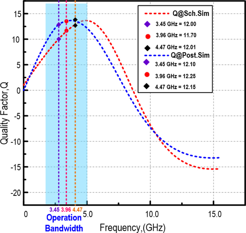
Figure 6: Simulated Q factor comparison between schematic (sch.sim) and post layout (post.sim).
C. Theory of operation of secondary core
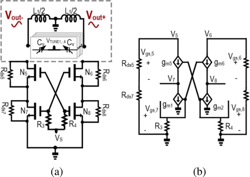
Figure 7: Secondary core (a) circuit and (b) small signal equivalent model.
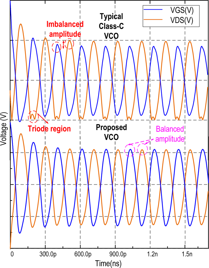
Figure 8: Simulated drain output voltage.
Figure 7 (a) exhibits the secondary core of the circuit sharing the gate bias for the four transistors N-N in a cascode configuration. In the half signal analysis depicted in Fig. 7 (b), the gain of each circuit is denoted as follows:
| (8) |
The high gain allows the auxiliary core to increase the signal’s amplitude, preserving the transistor’s saturation mode condition. Figure 8 depicts a balanced amplitude as opposed to the mismatched amplitude of a conventional class-C VCO.
III. PERFORMANCE RELIABILITY RESULTS
Figure 9 depicts the layout of the proposed VCO. The VCO occupies an active silicon area of 1.05 mm and consumes only 0.7 mW with supply voltage 1.2 V supply headroom.
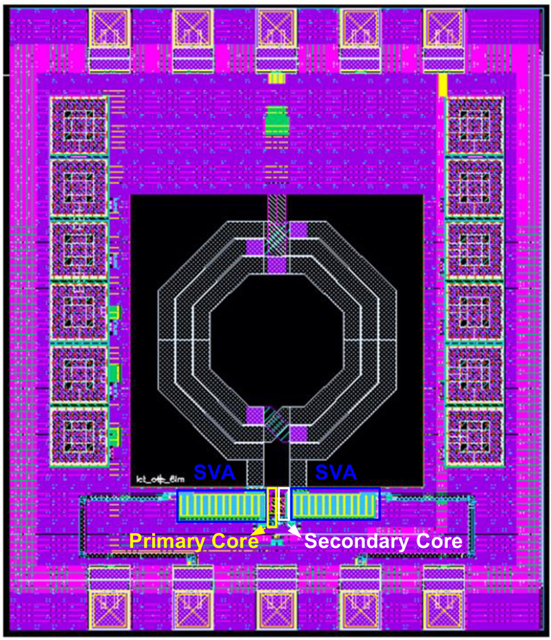
Figure 9: Layout of proposed VCO.
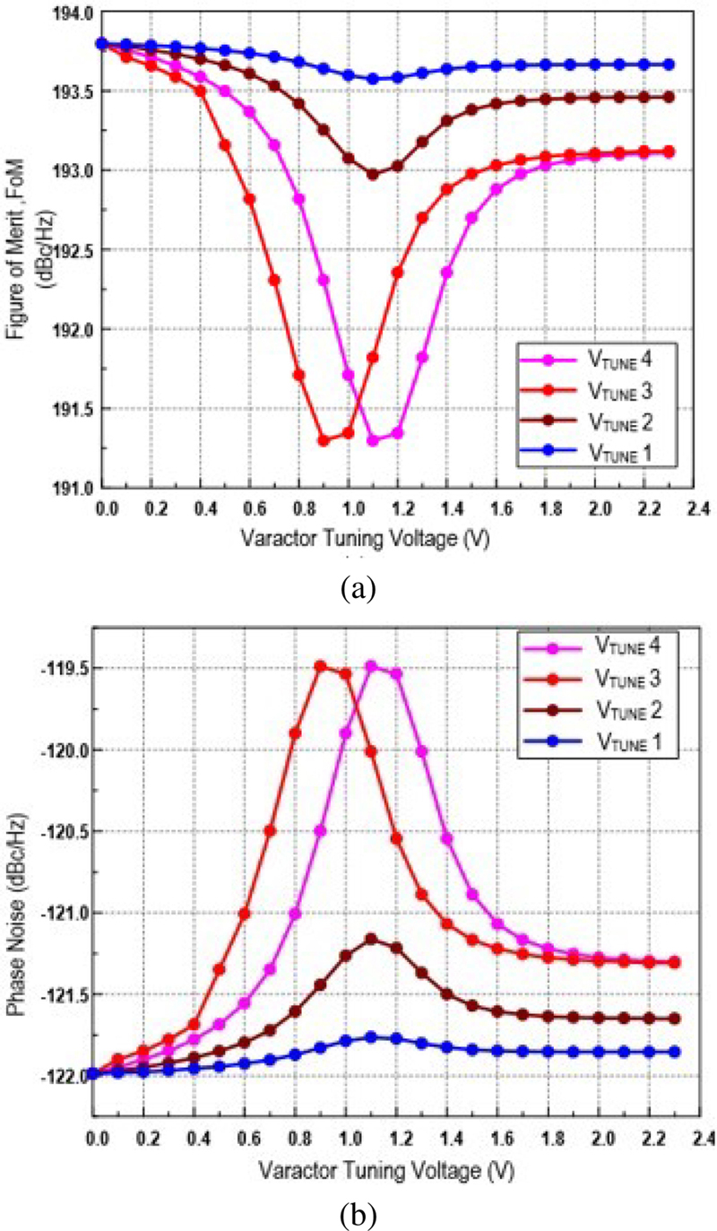
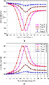
Figure 10: Simulated performance of the dual core VCO (a) FoM and (b) PN performance across the varactor tuning voltages V- VT.
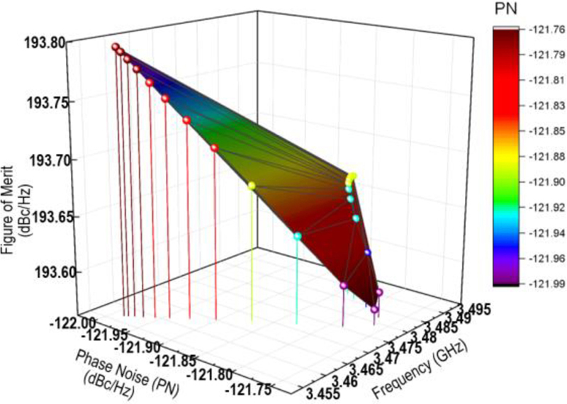
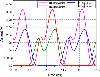
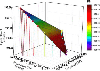
Figure 11: Relationship of Phase Noise (PN) with frequency and Figure of Merit (FoM).
Table 1: Performance comparison of the dual core VCO with other recent related works
| Performance Parameters | This Work | [16] | [17] | [18] | [19] | [20] |
| Frequency Range | ||||||
| Tuning Range | 32.43 | 29 | 13 | 12 | 42 | 41 |
| 1.2 | 1.8 | 1.5 | 0.55 | 1.2 | 1.1 | |
| Tech | 130 | 180 | 55 | 65 | 130 | 40 |
| Power Consumption | 0.7 | 18 | 6.3 | 5.0 | 5 | 6 |
| 2.3 | - | 2.1 | 1 | - | - | |
| PN | 121.25 | 119.5 | 121 | 117.5 | 119.21 | 112.63 |
| 193.25 | 174.6 | 185.05 | 187.2 | 184.9 | 185 |
[21]
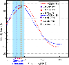
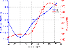
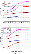
Figure 10 shows the simulated dual core in which Fig. 10 (a) shows the performance of the FoM and Fig. 10 (b) depicts the PN across the tuning voltages (V - V) where at under a suitable tuned bias of Vp and Vs at 647 mV and 600 mV respectively. The highest FoM obtained is at 193.79 dBc/Hz whereas the lowest PN is 122 dBc/Hz at frequency of 3.45 GHz under the tuning voltage of V. The relationship is further illustrated in Fig. 11. This 3D diagram shows the highest region of the phase noise, represented as blue, comprised the lowest phase noise level achieved, contributing to the highest FoM reading, while the red region comprised the higher phase noise reading reflecting towards a lower FoM level. With this tuned variable bias, it would be a degree of freedom to obtain for the best PN and FoM performance. Figure 12 shows the result of the PN and frequency across temperatures 40 to 125 C. At room temperature of 25 C, the phase noise achieved is in the range of 122 dBc/Hz to 122.5 dBc/Hz, however at the highest temperature of 125 C, the PN achieved is around 120.2 dBc/Hz. Nevertheless, for the frequency, the variation is only 300 MHz of difference across the temperatures. This shows that the performance of the PN and frequency are less impacted during the change in temperature, clearly proving its reliability. Figures 13 (a) and 13 (b) represent the frequency and the output power across the tuning voltages (V - V) respectively. The frequency bandwidth acquired results from 3.45 GHz to 4.47 GHz, whereas the boosted signal output power results from 5.7 dBm to 7.5 dBm. In this simulation, freedom is given to have multiple desired frequency and output power.
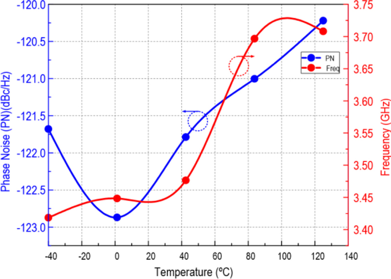
Figure 12: Simulated PN and frequency across temperature from 40 C to 125 C.
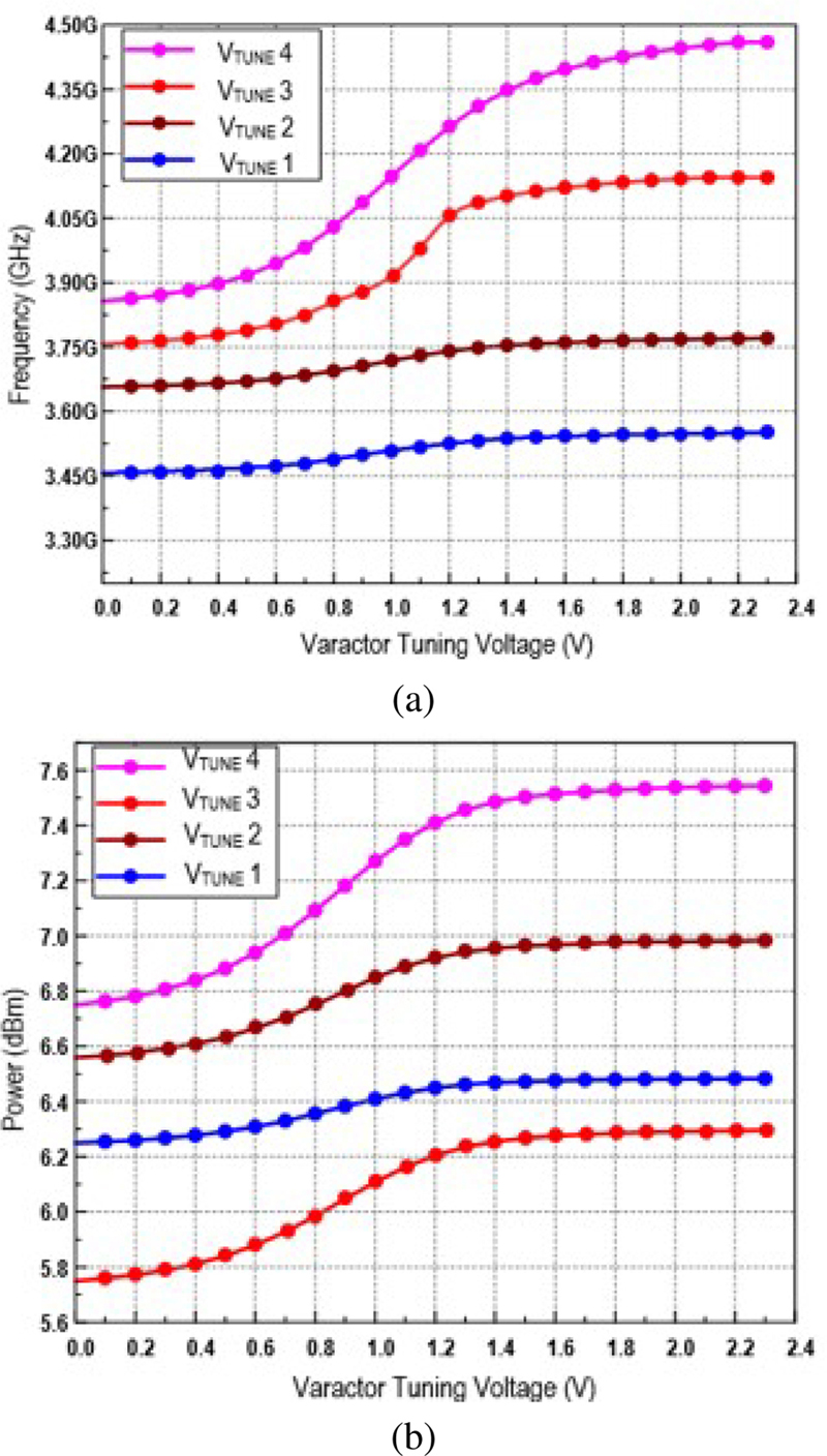
Figure 13: Performance of the dual core VCO (a) frequency (GHz) and (b) output power (dBm) across the varactor tuning voltages V- V.
Table 1 tabulates the performance comparison of the dual core VCO with other recent reported works. The proposed architecture leads other VCO performances by attaining high output swing and better phase noise reading performance using minimal powerconsumption.
IV. CONCLUSION
In this simulation work, a dual core VCO’s design has been demonstrated. Low phase noise performance is achieved by employing a Q enhancement technique in a cascoded structure in the primary auxiliary core. The VCO output swing is also improved by the secondary core merger. The proposed dual core VCO exhibits an output voltage swing of more than 2.0 V with a minimal supply voltage headroom of 1.2 V without significantly worsening its VCO phase noise across the operating bandwidth of 3.45 GHz to 4.47 GHz, as confirmed by both schematic and post layout simulation, which agrees well. Therefore, the presented architecture qualifies for use in 5G New Radio operations due to its low phase noise and low power consumption characteristics.
ACKNOWLEDGMENT
This work was supported by the Ministry of Higher Education Malaysia for Fundamental Research Grant Scheme with Project Code FRGS/1/2019/TK04/USM/02/14 and CREST under grant number PCEDEC/6050415.
REFERENCES
[1] M. Shahmohammadi, M. Babaie, and R. B. Staszewski, “Tuning range extension of a transformer-based oscillator through common-mode Colpitts resonance,” IEEE Trans. Circuits Syst. I, Reg. Papers, vol. 64, no. 4, pp. 836-846, Apr. 2017.
[2] D. Hauspie, E. C. Park, and J. Craninckx, “Wideband VCO with simultaneous switching of frequency band, active core and varactor size,” IEEE J. Solid-State Circuits, vol. 42, no. 7, pp. 452-455, July 2006.
[3] O. El-Aassar and G. M. Rebeiz, “A dual-core 8-17 GHz LC VCO with enhanced tuning switch-less tertiary winding and 208.8 dBc/Hz peak FoMT in 22nm FDSOI,” IEEE Radio Frequency Integrated Circuits Symposium (RFIC), Los Angeles, CA, USA, pp. 247-250, Aug. 2020.
[4] Y. Luo, C. Ma, Y. Gan, M. Qian, and T. Ye, “A dual-band CMOS LC-VCO with highly linear frequency tuning characteristics,” Microelectronics J., vol. 46, no. 12, pp. 1420-1425, June 2015.
[5] H. Amir-Aslanzadeh, E. J. Pankratz, C. Mishra, and E. Sanchez-Sinencio, “Current-reused 2.4-GHz direct-modulation transmitter with on-chip automatic tuning,” IEEE Trans. Very Large Scale Integr. Syst., vol. 21, no. 4, pp. 732-746, Apr. 2013.
[6] M. Fang, A. Kumura, and T. Yoshimasu, “A 210.4-dBc/Hz FoMT 67.9% tuning range LC-VCO IC with a single analog voltage-controlled novel varactor in 40-nm CMOS SOI,” IEEE International Symposium on Radio-Frequency Integration Technology, Hualien, Taiwan, pp. 2021-2023, Aug. 2021.
[7] B. Park, S. Lee, S. Choi, and S. Hong, “A 12-GHz fully integrated cascode CMOS LC VCO with Q-enhancement circuit,” IEEE Microwave and Wireless Components Letters, vol. 18, no. 2, pp. 133-135, Feb. 2008.
[8] H. Kim, S. Ryu, Y. Chung, J. Choi, and B. Kim, “A low phase-noise CMOS VCO with harmonic tuned LC tank,” IEEE Trans. Microw. Theory Tech., vol. 54, no. 7, pp. 2917-2923, July 2006.
[9] B. D. Williamson, “A 2.4 GHz LC-VCO using on-chip inductors and accumulation-mode varactors in a CMOS 0.18 m process,” Master’s thesis, University of Tennessee, Knoxville, TN, 2005.
[10] S. Chatterjee, Y. Tsividis, and P. Kinget, “0.5-V analog circuit techniques and their application in OTA and filter design,” IEEE J. Solid-State Circuits, vol. 40, no. 12, pp. 2373-2387, Dec. 2005.
[11] M. Fang and T. Yoshimasu, “A -197.3-dBc/Hz FoMT wideband LCVCO IC with a single voltage-controlled IMOS-based novel varactor in 40-nm CMOS SOI,” IEEE Trans. Microw. Theory Techn., vol. 68, no. 10, pp. 4116-4121, Oct. 2020.
[12] T. Azadmousavi and E. N. Aghdam, “A low power current-reuse LC-VCO with an adaptive body-biasing technique,” AEUE - Int. J. Electron. Commun., vol. 89, pp. 56-61, May 2018.
[13] T. Siriburanon, W. Deng, K. Okada, and A. Matsuzawa, “A current-reuse Class-C LC-VCO with an adaptive bias scheme,” IEEE Radio Frequency Integrated Circuits Symposium (RFIC), Seattle, WA, USA, pp. 35-38, June 2013.
[14] S. Ikeda, S. Lee, H. Ito, N. Ishihara, and K. Masu “A 0.5 V 5.96-GHz PLL with amplitude-regulated current-reuse VCO,” IEEE Microwave and Wireless Components Letters, vol. 27, no. 3, pp. 302-304, Mar. 2017.
[15] V. J. Higgins, F. A. Brand, and J. J. Baranowski, “Characteristics of varactor diodes biased into avalanche,” International Electron Devices Meeting, Washington, DC, USA, pp. 14-14, Oct. 1965.
[16] C. Sánchez-Azqueta, J. Aguirre, C. Gimeno, C. Aldea, and S. Celma, “High-resolution wide-band LC-VCO for reliable operation in phase-locked loops,” Microelectronics Reliability, vol. 63, pp. 251-255, Aug. 2016.
[17] M. Garampazzi, P. M. Mendes, N. Codega, D. Manstretta, and R. Castello, “Analysis and design of a 195.6 dBc/Hz peak FoM P-N class-B oscillator with transformer-based tail filtering,” IEEE J. Solid-State Circuits, vol. 50, no. 7, pp. 1657-1668, July 2015.
[18] Y. Peng, L. Zhou, Y. Yu, H. Liu, Y. Wu, C. Zhao, H. Tang, and K. Kang, “A harmonic-tuned VCO with an intrinsic-high-Q F23 inductor in 65-nm CMOS,” IEEE Microwave and Wireless Components Letters, vol. 30, no. 10, pp. 981-984, Oct.2020.
[19] C. H. Chun, H. S Choi, Q. D Bui, S. Y Kang, J. Y Jang, U. B. Lee, I. Y. Oh, and C. S. Park, “Compact wideband LC VCO with active inductor harmonic filtering technique,” Electronic Letters, vol. 47, no. 3, pp. 190-191, Feb. 2011.
[20] J. Du, X. Zhang, C. Zhang, F. Meng, and N. Yan, “An ultra-wideband VCO using digitally controlled varactor arrays in 40-nm CMOS technology,” IEEE MTT-S International Wireless Symposium (IWS), Nanjing, China, pp. 1-3, May 2021.
[21] P. Shasidharan, H. Ramiah, and J. Rajendran, “A 2.2 to 2.9 GHz complementary class-C VCO with PMOS tail-current source feedback achieving -120 dBc/Hz phase noise at 1 MHz offset,” IEEE Access, vol. 7, pp. 91325-91336, July 2019.
BIOGRAPHIES

Pravinah Shasidharan is currently pursuing a Ph.D. degree in microelectronics at the Universiti Sains Malaysia (USM), Pulau Pinang. Her research interest is in CMOS RFIC design.

Jagadheswaran Rajendran (SM’16) is currently serving as a senior lecturer at the Collaborative Microelectronic Design Excellence Center (CEDEC) and School of Electrical and Electronic Engineering, Universiti Sains Malaysia. His work is on CMOS analog IC design, CMOS Radio Frequency (RF) IC design and GaAs Monolithic Microwave Integrated Circuit (MMIC) design. To date, he has published 70 research papers, mainly in journals, and holds one US patent. Jagadheswaran Rajendran was the recipient of the IEEE Circuit and System Outstanding Doctoral Dissertation Award in 2015. He served as the Chairman of IEEE ED /MTT/SSC Penang Chapter for the years 2011 and 2018. He is also a senior member of IEEE.

Selvakumar Mariappan received his B. Eng. Tech. Degree (Hons.) in electrical engineering technology from the Technical University of Malaysia Melaka (UTeM) in 2017. He completed his Ph.D. degree in microelectronics system engineering from Universiti Sains Malaysia in 2022. He was a scholarship recipient of the Industry Graduate Research Assistant Scholarship Programme (i-GRASP) from CREST R&D, Malaysia. Selvakumar Mariappan was a post-graduate intern in Silterra Malaysia Sdn. Bhd. from 2018 to 2021 where he was involved in various IC design activities from device modelling to IC measurements. He was with QRF Solutions Sdn. Bhd. from May 2021 to August 2022 as an IC designer where he worked on numerous RFIC design projects. He served as a Post-Doctoral Fellow at the Collaborative Microelectronic Design Excellence Center (CEDEC), Universiti Sains Malaysia from September to November 2022 before being promoted to Senior Lecturer there in December 2022.

Narendra Kumar received his doctorate degree in electrical engineering from RWTH Technical University Aachen, Aachen, Germany. From early 1999 he was with Motorola Solutions, holding the position of Principal Staff Engineer (product development and testing). Since January 2011 he has been a Visiting Professor to Istanbul University. Since August 2013, he has been with the Department of Electrical Engineering at the University of Malaya, serving as an Associate Professor. He holds three US patents and four defensive patents in the area of microwave power amplifiers, all assigned to Motorola Solutions. He has authored more than 80 papers in technical journals and conferences, and three technical books published in the USA.

Masuri Othman received his master’s degree in optoelectronics from the University of Essex, UK, and his Ph.D. degree in microelectronics from the University of Southampton, UK. His main research interests are intheareas of microelectronics and IC design, energy harvesters and technology planning and commercialization. He joined the National University of Malaysia in 1978, was promoted to an Associate Professor in 1989, and subsequently in 1996 to the post of a Professor in microelectronics. He was the Deputy Director of the Institute of Micro and Nanoelectronics (IMEN), UKM, from 2004 to 2006. He was on secondment to the Malaysian Institute of Microelectronics (MIMOS) from 2005 to 2011 as the Director of MEMS and Nanotechnology and at the same time has produced more than 20 patents mainly in the areas of MEMS and energy harvesting. From 2011 to 2014, he was the Commercialization Director at the Ministry of Science and Technology, Malaysia. In 2016, he rejoined IMEN with the main task of spearheading frontier research as well as the technology commercialization of the research and development. During his tenure he has produced more than 100 research papers and has won several national awards in his research areas.
ACES JOURNAL, Vol. 38, No. 6, 457–465
doi: 10.13052/2023.ACES.J.380610
© 2023 River Publishers