Wideband Iris-Fed Patch Antenna Under Operation of Dual-Resonance for X-band Applications: MOM-GEC Approach
M. Abdi and T. Aguili
Sys’Com Laboratory
National Engineering School of Tunis, Tunis El Manar University, BP 37, le Belvédère, Tunisia
mariemahmedabdi@gmail.com, taoufik.aguili@enit.utm.tn
Submitted On: September 20, 2022; Accepted On: February 24, 2023
ABSTRACT
In this paper, a microstrip patch antenna fed by a waveguide using an end-wall iris through ground plane has been modelled. The iris feed technique was proposed to overcome the narrow bandwidth problem of microstrip patch antenna. The iris is sized so that it is resonant and subsequently the antenna operates under the fusion of two modes relating to the iris and the patch, resulting in a wideband radiation characteristic with dual resonance. Measurement demonstrates the single bandwidth dual resonance type and the radiation bandwidth of (8 GHz-10.6 GHz). In order to show the impact of the iris feed technique on microstrip patch antenna’s bandwidth, a comparison with some state-of-the-art works proposing various bandwidth enhancement techniques in the X-band is made. The proposed prototype, with a size of 1.761.651.29, is more compact than several designs. It has a fractional bandwidth of 27.9%, thus it presents the prototype with the widest bandwidth with the simplest design fabrication. With regard to the electromagnetic modelling, this work is oriented towards the use of the hybrid MOM-GEC method in order to be able to perform a rigorous electromagnetic. It has been found that the MOM-GEC model is more efficient in terms of memory requirements and approximately four times faster than HFSS simulator software.
Index Terms: bandwidth, dual-resonance, iris-fed patch antenna, MOM-GEC analysis, wideband, X-band.
I. INTRODUCTION
Communication systems in the X-band require the design of antennas characterized by higher gains and wide bandwidths.
The microstrip patch antenna presents a good candidate for its low weight, its small size, the ease of its manufacture and its integration, etc. However, one of the major disadvantages is its low gain and its low bandwidth, which is of the order of a few percent (2% to 4%).
Multiple techniques have been used to widen the bandwidth of microstrip antennas, namely: the thick substrate, the partial substrate removal, the superstrate cover [1–2], the parasitic patches coupled to the main patch or stacked patches [3], the patch with metallic rings, the defected ground structure, the reflecting layer, the electromagnetic band gap as material [4], the merging of several antenna resonance modes [5–6], etc.
The microstrip patch antenna’s type of alimentation has an impact on its bandwidth as well. The iris feed technique is used to increase the patch bandwidth in order to get over the issue of narrow bandwidth [7–8]. The iris-fed microstrip patch antenna is equivalent to an antenna having two patches, one of which radiates toward the open end of the rectangular waveguide and the other toward open air. Therefore, this structure combines appealing characteristics of a microstrip antenna, like low profile, light weight, compact size, and simple integration in electronic circuits, with those of a waveguide, like high power handling capacity and low losses (resistive) [9]. In this method, the waveguide’s mouth is directly fitted with the microstrip antenna. As a result, the most energy is radiated.
Apart from the techniques for enlarging the bandwidth of the microstrip patch antenna, several antenna parameters intervene to achieve the maximum achievable bandwidth, namely: the height of the antenna cavity [10–11]., the thickness of the substrate or of the superstrate [12], the spacing between the main patch and the parasitic patches, etc.
From the above literature survey, this work proposes to model a microstrip patch antenna fed by a waveguide using an end-wall iris through ground plane since it has not been widely used in X-band. The iris is sized so that it is resonant and subsequently the antenna operates under the fusion of two modes relating to the iris and the patch [13], resulting in a wideband radiation characteristic with dual resonance.
Regarding the state-of-the-art works for the iris-fed patch antenna’s electromagnetic modelling, it turns out that the current trend is to use simulation tools such as HFSS and CST which are essentially based on methods that require a 3D mesh [14]. Other works have been based on numerical models as in [7, 8] which used the modal expansion model and the method of Moments respectively. These integral methods are best suited to perform an electromagnetic modelling of planar microwave structures. However, when the complexity of the structures increases, the resolution becomes complicated, and this requires more memory space and computation time.
Several research works [15, 16] have focused on the use of hybrid methods to improve the conventional methods. In fact, their major interest lies in the ability to solve complex structures whereas neither a single numerical method nor commercial software can model them correctly. In this context, this work is oriented towards modelling the proposed antenna based on MOM-GEC numerical technique. This latter handles complex electromagnetic structure as no mesh is required, thus, a gain is achieved in terms of computational time and memory storage.
This paper is divided as follows. Section II introduces the numerical technique formalism and the antenna description. The mathematical formulation based on the hybrid approach will be detailed in Section III. Section IV presents the validation of the antenna by full-wave simulations. To confirm the accuracy and the efficiency of the proposed numerical approach, a comparison with HFSS and with measurement is held. Finally, Section V concludes the work.
II. THEORETICAL BACKGROUND
A. MOM-GEC approach
In [17], Baudrand proposed the hybridization of the method of Moments (MOM) with the method of Generalized Equivalent Circuits (GEC) in order to be able to perform a rigorous electromagnetic calculation while minimizing the execution time and the required memory resources. The equivalent circuits were introduced in the development of the formulation of integral methods in an attempt to transpose field problems into equivalent circuit problems that are generally easier to deal with [18, 19].
The hybrid MOM-GEC is therefore considered to be a true electrical image of the structure to be studied since it faithfully describes the discontinuity as well as its environment:
The wave which excites the surface of discontinuity is represented symbolically by a source (localized or modal) of field or current called real since it delivers power.
At the level of the discontinuity, the electromagnetic state is described by generalized test functions which are modelled by virtual sources not storing energy. The virtual field source must be adjustable so as to cancel the dual magnitude (the transverse current of this source) and vice versa.
The discontinuity environment is expressed by an impedance/admittance operator which represents the boundary conditions on either side of the discontinuity surface.
The auxiliary sources (AS) make it possible to interconnect two distinct parts of a circuit when they are of different dimensions from each other [20, 21].
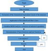
Once the equivalent circuit is extracted, the implementation of the proposed MOM-GEC steps is described in the flowchart as illustrated in Fig. 1.
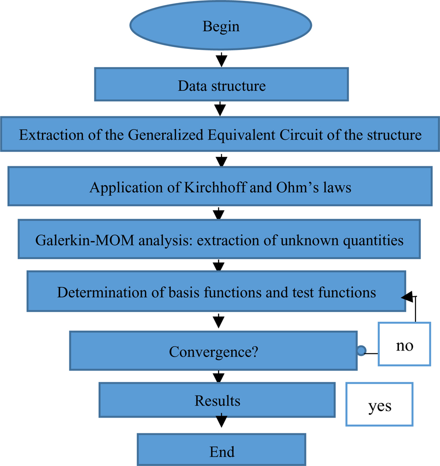
Figure 1: Flowchart of the MOM-GEC method.
It should be noted that the computer code of the numerical method is translated with MATLAB and executed on an Intel Core i7 processor computer with a processing capacity of 2.7 GHz and 8 GB RAM.
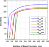
The convergence study is essential in a first step for the validation of the numerical method MOM-GEC. It is carried out through the determination of the number of test functions and the number of basis functions which have to be fixed in such a way that the boundary conditions of the electromagnetic state of the antenna is verified. Once these parameters are found, they will be used in the rest of the calculation to extract the characteristics of the antenna. In fact, the exact solution is provided only at the convergent state of the structure’s parameter that we can consider it as a steady state.
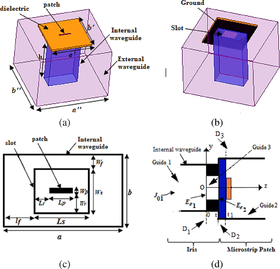
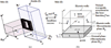
Figure 2: (a) Iris-fed patch antenna. (b) Bottom view. (c) Top view. (d) Side view: , (dielectric thickness)=1.6, (ground and patch thickness) , (all dimensions in millimeters),.
B. Antenna description
The antenna illustrated in Fig. 2 is composed of a three-layer device which consists of a dielectric layer sandwiched between a radiating patch and a ground plane. The structure is fed by an iris which is formed by an obstacle pierced with a rectangular coupling slot and terminating a rectangular waveguide. The presence of the conductive ground plane leads the electromagnetic radiation to be oriented from the exciter waveguide to the patch through the coupling slot. The feeder waveguide is excited by the fundamental mode and the microstrip patch antenna is excited by the quasi-TEM mode.
III. MOM-GEC PROBLEM FORMULATION
A. Generalized equivalent circuit
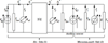
The antenna is composed of the iris and a microstrip patch interconnected through the auxiliary sources (AS), as illustrated in Fig. 3. Note that the external waveguide is not considered when modelling the structure since the excitation by the mode is done through the internal waveguide.

(a)(b)
Figure 3: (a) Iris located between two virtual waveguides at (z=0), each of which is characterized by perfect electrical walls (EEEE) on all faces. (b) Patch shielded in rectangular waveguide defined by perfect electrical walls (EEEE) on all faces.
The centered thick iris, as shown in Fig. 3 (a), is located between two virtual waveguides at (z=0), each of which is characterized by two electric side walls and two electric horizontal walls (which will be identified by EEEE for four times Electrical). These two waveguides are: the entry virtual waveguide (Guide 1) and the exit virtual waveguide (Guide 2), which do not have the same height.
The microstrip patch is placed in the cross section of a rectangular waveguide at (z=) open to infinity. The boundary conditions are defined by perfect electrical walls on all sides as shown in Fig. 3 (b).
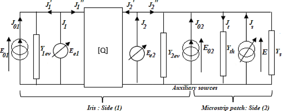
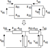
Figure 4: GEC of the antenna using the MOM-GEC technique.
The whole structure represents three planes of discontinuity, respectively in z=0, in z=t, and in z=, as illustrated in Fig. 2 (d). Each discontinuity includes two subdomains: the metal and the dielectric. By placing ourselves on the plane of discontinuity , we solve the equivalent scheme GEC of Fig. 4.
On side (1), the real current source and the real field source are expressed respectively according the amplitude and and according the fundamental mode of the modal base function [22]:
| (1) |
| (2) |
The auxiliary current source and the auxiliary field source are expressed respectively according the amplitude and and according the fundamental mode of the modal base function :
| (3) |
| (4) |
Discontinuities and are identical so they have the same test function which is similar to the fundamental mode in the iris. The virtual electric fields and are equals and expressed in terms of test function and weighting coefficients [23]:
| (5) |
The thick rectangular iris between two guides of different heights can be subdivided into three guides [24] (see Fig. 2 (d)).
Guide 1
The admittance of the modal source representing the evanescent modes at the level of discontinuity of the exciter waveguide which is associated with the modal base function is expressed by [25]:
| (6) |
| (7) |
Guide 2
The admittance of evanescent modes respectively related to the modal source at the level of discontinuity of the second waveguide which is associated with the modal base function is expressed by:
| (8) |
| (9) |
Guide 3
The line length between the two discontinuities and is represented by [26]:
| (10) |
The input admittance and the inverse transfer admittance of quadrupole associated with the modal base function are respectivelyexpressed by:
| (11) |
| (12) |
| (13) |
On side (2), the virtual current distribution which is the dual of virtual electric field E, is expressed in terms of test function and weighting coefficients:
| (14) |
The admittance of the dielectric layer is expressedby [27]:
| (15) |
The admittance from the vacuum brought to the surface of the dielectric is expressed by:
| (16) |
| (17) |
B. Kirchhoff and Ohm’s laws
On side (1), the application of Ohm’s and Kirchhoff’s law to the equivalent circuit leads to obtain the following equations given by:
| (18) |
| (19) |
therefore, the virtual current sources and are expressed as:
| (20) |
| (21) |
| (22) |
On side (2), as the dielectric is thin, it is equivalent to a layer surface impedance. Then, by applying Ohm’s and Kirchhoff’s laws, the auxiliary electric field and the virtual electric source E are given by:
| (23) |
| (24) |
The total admittance of the circuit is the sumof .
C. Application of Galerkin method
The resolution of electromagnetic equations is provided by (V, I) physical scales instead of using (E, J) physical scales [28]. Therefore, Fig. 3 is presented as illustrated in Fig. 5.
Figure 5: GEC of the antenna using the MOM-GEC technique using (V, I) physical scales.
The projection of equations (18) and (19) on the test functions with the cancellation of virtual current source and is solved by the method of Galerkin as it is indicated in the matrix system (25):
| (25) |
noting that is the vector ponderation expressed by , is the first excitation vector expressed by , is the second excitation vector expressed by , is the first impedance matrix expressed by , is the second impedance matrix expressed by and is the third impedance matrix expressed by .
Noting that:
| (26) |
the expression of the input impedance (27) is deduced from (25):
| (27) |
the magnitude in (dB) of the reflection coefficient is deduced from (27) as expressed in (28a):
| (28a) |
The angle in (degree) of the reflection coefficient is deduced from (28a) as expressed in (28b):
| (28b) |
where is the impedance of fundamental mode and is the phase.
The projection of the equation (23) and (24) on the test functions with the cancellation of virtual current distribution is solved by the method of Galerkin as it is indicated in the matrix system (29):
| (29) |
noting that , is the excitation vector expressed by , and is the impedance matrix which define the coupling between p and q dielectric elements and expressed by .
From (29), the expression of is deduced:
| (30) |
The amplitude is expressed as:
| (31) |
| (32) |
IV. COMPUTED RESULTS
A. Convergence study
The convergence of the input impedance and the antenna current is established for the test function number =11 and the number of modes =300 as mentioned respectively in Fig. 6 and Fig. 7.
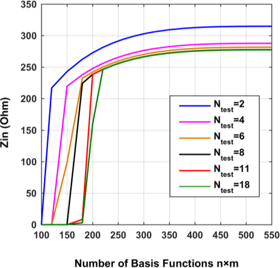
Figure 6: Input impedance as a function of different number of and .
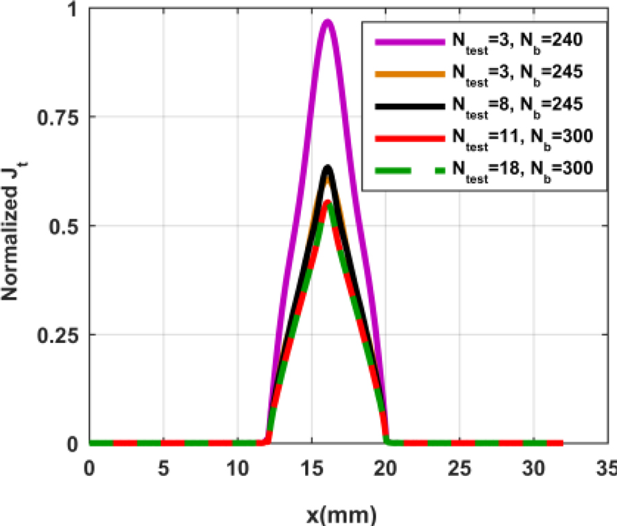
Figure 7: Current distribution as a function of different number of and .
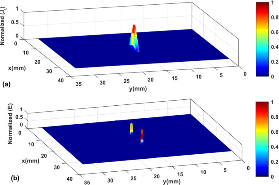
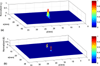
Figure 8: (a) Normalized current distribution of the antenna. (b) Normalized electric field of antenna obtained at convergence.
B. Boundary conditions verification
Figure 8 illustrates the current distribution and electric field of the antenna which are consistent with electromagnetic field theory. In Fig. 8 (a), the current density distribution is shown at the metallic patch. In Fig. 8 (b), the normalized electric field peak is at the edge of the patch in the x direction and the minimum values are at the dielectric.
C. Antenna’s characteristics
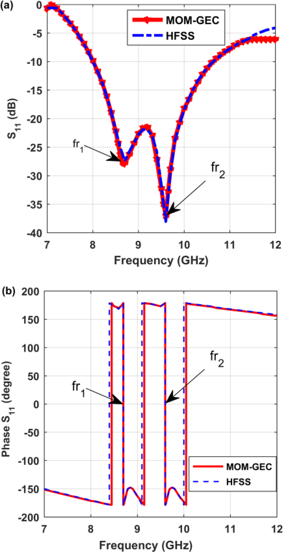
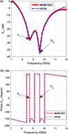
Figure 9: (a) Magnitude in dB, and (b) the angle in degree of reflection coefficient of the antenna compared to HFSS.
Figure 9 illustrates both the magnitude in dB and the angle in degree of reflection coefficient of the antenna. To confirm the accuracy and the efficiency of the proposed numerical approach, a comparison with HFSS is held. It shows a slight difference between results due to different numerical techniques used.
The simulated reflection coefficient of the proposed antenna has two resonance frequencies as illustrated in Fig. 9 (a); one appears at =8.7 GHz and the other appears at= 9.6 GHz, so the bandwidth is centered around = 9.15 GHz.
The frequency study on the phase of the reflection coefficient shows there are two modes whose resonance frequencies are and where the phase of the reflection coefficient is zero (see Fig. 9 (b). Note that each resonance is determined where the phase of the reflection coefficient is zero.
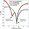
In order to identify each mode, a study was carried out on the reflection coefficient of the iris alone [24] and then on that of the total structure. As presented in Fig. 10, the iris alone presents a first resonance at 9.6 GHz. By adding the dielectric and the patch above the iris, a second resonance frequency at 8.7 GHz appears at a frequency lower than. Due to the merging of the modes relating to the iris and the patch, a wideband radiation characteristic with dual-resonance is obtained.
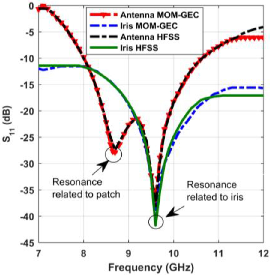
Figure 10: Simulated reflection coefficients of the iris alone and the iris-fed antenna as a function of frequency.
In order to show the calculation efficiency of the proposed method, CPU time and storage memory required by MOM-GEC and HFSS simulator have been reported in Table 1. It has been found that the MOM-GEC model is more efficient in terms of memory requirements and approximately four times faster than HFSS simulator software.
Table 1: Comparison of CPU time between the MOM-GEC method and the HFSS simulator (Intel Core i7 with a processing capacity of 2.7 GHz and 8 GB RAM)
| CPU Time (in seconds) | Memory Requirements (GB) | ||
|---|---|---|---|
| HFSS | This Paper | HFSS | This Paper |
| 1276 | 340 | 3.04 | 0.18 |
D. Antenna fabrication and comparison with various X-band antennas
The prototype of the fabricated iris-fed patch antenna as shown in Fig. 11. The antenna is excited by a rectangular waveguide of the Oritel TGN R100/WR90 type with 22.86 mm 10.16 mm 41.5 mm dimension, also extended wall dimension is 56.5 mm 53mm.
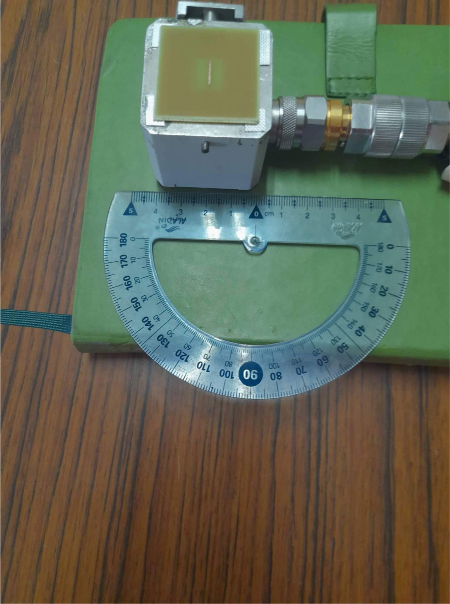
Figure 11: Photograph of the fabricated iris-fed microstrip patch antenna.
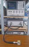
As illustrated in Fig. 12, the results are measured by an Agilent HP 8510C vector network analyzer (VNA) whose characteristics are described in [29].
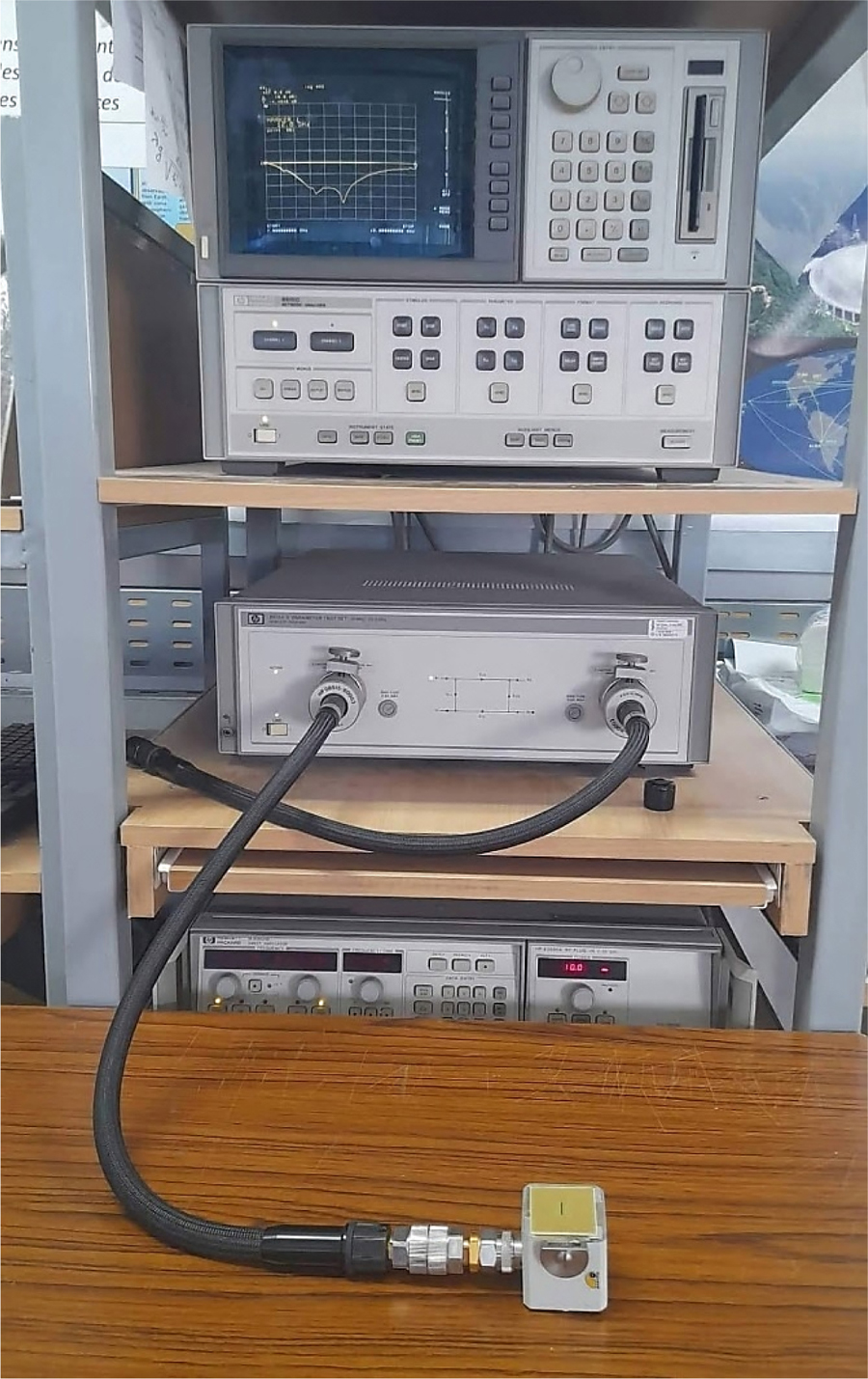
Figure 12: Photograph of measurement set-up: Reflection coefficient measurement.
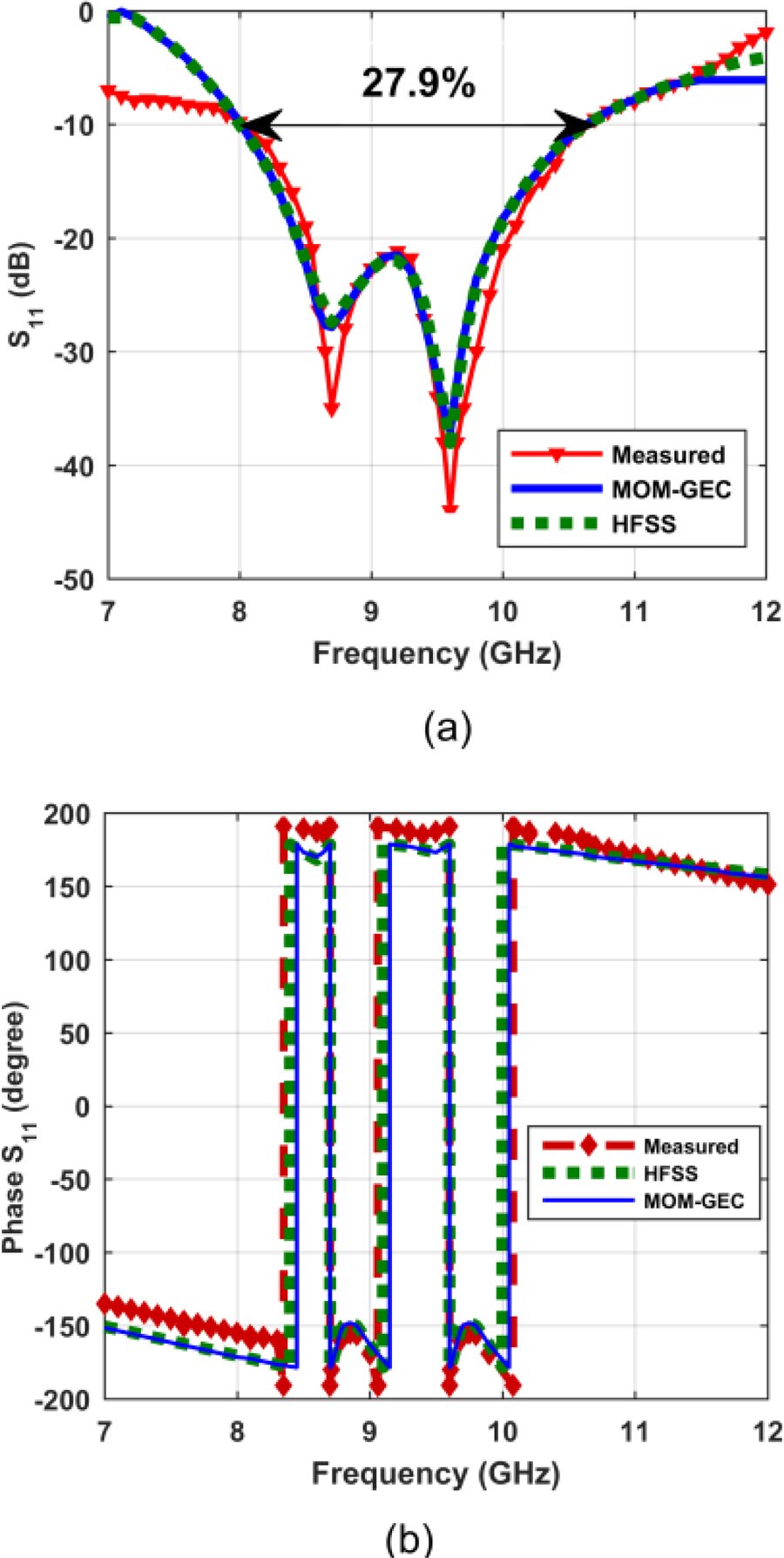
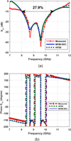
Figure 13: (a) Magnitude in dB, and (b) the angle in degree of simulated and measured reflection coefficient of the antenna.
Table 2: Performances comparison of the proposed antenna with the state-of-the-art works operating in the X-band
| Ant | Bandwidth Enhancement Technique | Dimension in | Band Type | -10 dB Fractional Bandwidth (GHz;%) | Design Complexity | Modelling Technique |
| [30] | Metallic superstrate | Single* | HFSS | |||
| [31] | Dielectric superstrate | Single | CST | |||
| [32] | Parasitic patch above foam | Single* | CST | |||
| [33] | Dielectric superstrate | Single* | HFSS | |||
| [1] | Compact Partially Reflective Surface | Single | HFSS | |||
| [2] | AMC ground plane and a FSS superstrate | Single | NA | |||
| [4] | Metamaterial substrate | Single* | NA | |||
| [34] | Cavity backed structure | Single | HFSS | |||
| [14] | Air cavity | Single | NA | |||
| This work | Resonant iris as feeding technique | Single* | MOM-GEC + HFSS |
Ant: Antenna; W LT: WidthLengthThickness; SIW: Substrate integrated waveguide; Single*: Single with dual-resonance; AMC: Artificial Magnetic Conductor; FSS: Frequency Selective Surface; (++): Very high; (+) High; (-) Low; NA: not mentioned; HFSS: High Frequency Simulation Software; CST: Computer Simulation Technology.
Figure 13 illustrates both the magnitude in dB and the angle in degree of simulated and measured reflection coefficient of the antenna. Measurement demonstrates the single band with dual resonances type (8.7GHz and 9.6GHz) and the radiation bandwidth of (8GHz-10.6GHz).
A slight difference between the simulated and measured results is marked especially between 7GHz and 8GHz. This may be due to the manufacturing tolerance and the effect of the connector which was not taken into account in the design with HFSS and when modelling with the numerical method. Integrating the connector into MOM-GEC modelling and in the HFSS design could be a solution to further minimize this difference.
A comparison of performance characteristics between the proposed antenna and the state-of-the-art works operating in the X-band is listed in Table 2.
Without the addition of superstrate cover, the antenna bandwidth is equal to 5.8% and 11.1% respectively in [30, 33]. Hence, the interest of adding superstrate cover as a bandwidth expansion technique. Indeed, the superstrate cover can be either dielectric, metallic, metamaterial, frequency selective surface. In [32], a stacked microstrip patch antenna has been presented. The addition of parasitic patch above foam compared to the main patch increased its bandwidth from 7.54%to 16.2%.
The proposed antenna has a smaller volume than[2, 30–33]. Moreover, it has the highest impedance bandwidth and the simplest design fabrication. Due to its high bandwidth, its simple fabrication, and its compactness, this antenna represents a promising candidate for X-band satellite communication, radar application, microwave power transmission, and wireless communication.
The state-of-the-art works mentioned in Table 2 have used simulation tools such as HFSS and CST which are essentially based on methods requiring a 3D mesh. This work is characterized by studying the antenna structure based on an analysis method, which makes it possible to convert a 3D investigation problem into a 2D investigation problem and, subsequently, to minimize the execution time and the memory resources required.
V. CONCLUSION
In this work, the modelling of dual-resonant antenna with closely spaced resonance frequencies for bandwidth enhancement has been investigated for X-band applications. The antenna consists of a microstrip patch antenna fed by a waveguide using an end-wall iris through ground plane. The antenna has a size of 1.761.651.29, and has a fractional bandwidth of 27.9%.
The antenna is modelled by the hybrid MOM-GEC method. Equivalent circuits (GEC) are introduced in the development of the formulation of integral methods in an attempt to transpose field problems into equivalent circuit problems that are generally easier to deal with. Consequently, a reduction in both memory requirements and computation time is achieved. The problem thus formulated, its numerical resolution is done by applying Galerkin’s method, which is known for the simplicity of its formulation.
This procedure is, in fact, general and it can be applied to the study of several electromagnetic problems, namely: the uniaxial discontinuity in waveguides, the multiaxial diffraction discontinuities in free space, the antenna radiation, the circuits comprising localized sources, etc. Moreover, the proposed hybrid method can be extended to become a multi-scale method. The techniques for solving each electromagnetic problem essentially differ from each other in the development of the operators involved. Admittedly, the theoretical basis and the approach to be followed remain unchanged. This is due to the fact that the methods used are in all cases integral methods.
REFERENCES
[1] F. Meng and S. K. Sharma, “A wideband resonant cavity antenna with compact partially reflective surface,” IEEE Trans. Antenn. Propag., vol. 68, no. 2, pp. 1155-1160, 2020.
[2] R. Fakhte and I. Aryanian, “Compact Fabry-Perot antenna with wide 3-dB axial ratio bandwidth based on FSS and AMC structures,” IEEE Antennas Wirel. Propag. Lett, vol. 19, no. 8, pp. 1326-1330, 2020.
[3] H. Hung Tran and N. Nguyen-Trong, “Performance enhancement of MIMO patch antenna using parasitic elements,” IEEE Access, vol. 9, pp. 30011-30016, 2022.
[4] O. Borazjani, M. Naser-Moghadasi, J. Rashed-Mohassel, and R. A. Sadeghzadeh, “Bandwidth improvement of planar antennas using a single-layer metamaterial substrate for X-band application,” Intern. Journ. Micro. Wirel. Tech., vol. 12, no. 9, pp. 906-914, 2020.
[5] X. Zhang, T. Tan, Q. Wu, L. Zhu, S. Zhong, and T. Yuan, “Pin-loaded patch antenna fed with a dual-mode SIW resonator for bandwidth enhancement and stable high gain,” IEEE Antennas Wirel. Propag. Lett., vol. 20, no. 2, pp. 279-283, 2021.
[6] X. Liu, W. Hu, S. Gao, L. Wen, Q. Luo, R. Xu, and Y. Liu, “A wideband triple-mode differentially fed microstrip patch antenna,” IEEE Antennas Wirel. Propag. Lett.,” vol. 20, no. 7, pp. 1160-1164,2021.
[7] M. Kanda, D. Chang, and D. Greenlee, “The characteristics of iris-fed millimeter-wave rectangular microstrip patch antennas,” IEEE Trans. Electro. Compat., vol. 27, no. 4, pp. 212–220, 1985.
[8] K. K. Sood, R. Jyoti, and S. B. Sharma, “A waveguide shunt slot-fed microstrip patch antenna—analysis using the method-of-moments,” IEEE Trans. Antenn. Propag., vol. 61, no. 1, pp. 5385-5394, 2013.
[9] A. Omar, M. Hussein, I. Rajmohan, and K. Bathich, “Dual-band MIMO coplanar waveguide-fed-slot antenna for 5G communications,” Heliyon, vol. 7, no. 4, pp. 1-10, 2021.
[10] N. C. Karmakar, “Investigations into a cavity-backed circular-patch antenna,” IEEE Trans. Antenn. Propag., vol. 50, no 12, pp 1706-1715, 2002.
[11] M. Martinis, K. Mahdjoubi, R. Sauleau, S. Collardey, and L. Bernard, “Bandwidth behavior and improvement of miniature cavity antennas with broadside radiation pattern using a metasurface,” IEEE Trans. Antenn. Propag., vol. 63, no. 5, pp. 1899-1908, 2015.
[12] M. A. K. Khan, M. I. Ullah, R. Kabir, and M. A. Alim, “High-performance graphene patch antenna with superstrate cover for terahertz band application,” Plasmonics, vol. 15, pp. 1719-1727,2020.
[13] P. K. Malik, S. Padmanaban, and J. B. Holm-Nielsen, Microstrip Antenna Design for Wireless Applications, 1st ed., CRC Press: Boca Raton, USA, 2021.
[14] R. Fakhte and I. Aryanian, “High gain and wideband patch antenna with wide 3-dB axial ratio bandwidth operating at TM01 and TM11 modes,” IET Micro. Antenn. Propag. Journ., vol. 15, no. 4, pp. 389-396, 2021.
[15] Y. Zhong, H. Wang, W. Huang, W. Xu, J. Xu, and J. Dai, “A hybrid loop-tree FEBI method for low-frequency well logging of 3-D structures in layered media,” IEEE Trans. Geo. Rem. Sens., vol. 60, pp. 1-9, 2021.
[16] J. Ma, S. Gong, X. Wang, Y. Liu, and Y. Xu, “Efficient wide-band analysis of antennas around a conducting platform using MoM-PO hybrid method and asymptotic waveform evaluation technique,” IEEE Trans. Antenn. Propag., vol. 60, no. 12, pp. 6048-6052, 2021.
[17] H. Baudrand, Introduction au calcul des éléments de circuits passifs en hyperfréquences, Cépaduès Éditions, Toulouse, 2001.
[18] S. Smirani, M. Aidi, S. Mili, and T. Aguili, “Electromagnetic modeling of rectenna based on the hybrid MoM–GEC combined to the harmonic balance method for wireless power transmission,” Journ. Electro. Wav. App. , vol. 34, no. 6, pp. 697-714, 2020.
[19] H. Helali, S. Smirani, M. Aidi, and T. Aguili, “Electromagnetic modeling of reconfigurable antenna array for 5G communications. Journal of Electromagnetic Waves and Applications,” Journ. Electro. Wav. App. , vol. 35, no. 17, pp. 2368-2383, 2021.
[20] K. Minas, L. Nikolaos, and F. George, “Method of auxiliary sources with an excitation source: The auxiliary-current vector norm,” IEEE Micro. Wirel. Comp. Lett., vol. 29, no. 10, pp. 1-4, 2021.
[21] K. Minas, L. Nikolaos, and F. George, “Mode analysis by the method of auxiliary sources with an excitation source,” IEEE Trans. Micro. Theory Tech., vol. 69, no. 6, pp. 2960-2971, 2021.
[22] T. Aguili, Modélisation des composants S. H. F planaires par la méthode des circuits équivalents généralisés, Department of Electrical Engineering, National Engineering School of Tunis ENIT, 2000.
[23] H. Baudrand, “Representation by equivalent circuit of the integral methods in microwave passive elements,” Eur. Micro. Conf., Hungary, 9-13 Sep., 1990.
[24] N. Raveu and O. Pigaglio, Résolution de problèmes hautes fréquences par les schémas équivalents, Cépaduès Éditions, Toulouse, pp. 127-146, May2012.
[25] Z. Mekkioui and H. Baudrand, “Bi-dimensional bi-periodic centred-fed microstrip leaky-wave antenna analysis by a source modal decomposition in spectral domain,” IET Micro. Antenn. Propag. Journ., vol. 3, no. 7, pp. 1141-149, 2009.
[26] H. Baudrand and D. Bajon, “Equivalent circuit representation for integral formulations of electromagnetic problems,” Int. Journ. Num. Model.-Elect. Net. Dev. Fields, vol. 15, no. 1, pp. 23-57, 2002.
[27] H. Helali, M. Aidi, and T. Aguili, “Electromagnetic modelling of multiband frequency reconfigurable antenna for wireless communications,” Journ. Electro. Wav. App., vol. 34, no. 5, pp. 634-654, 2020.
[28] Z. Chen, C. Wang, and W. Hoefer, “A unified view of computational electromagnetics,” IEEE Trans. Micro. Theory Tech., vol. 70, no. 2, pp. 955-969, 2022.
[29] Agilent Technologies 8510C Network Analyzer System: Operating and Programming Manual, Editions 3, USA, 2001.
[30] R. Fakhte and H. Ghorbaninejad, “High gain and improved waveguide slot antenna using a metallic superstrate as main radiator,” IET Micro. Antenn. Propag., vol. 11, no. 8, pp. 563-557,2016.
[31] T. Rahim and J. Xu, “Design of high gain and wide band EBG resonator antenna with dual layers of same dielectric superstrate at X-bands,” Journ. Micro., Opto. Electro. App. , vol. 15, no. 2, pp. 93-104, Jun. 2016.
[32] R. Fakhte and H. Ghorbaninejad, “High-gain waveguide slot antenna using simple parasitic patch’s cover,” Int. Journ. RF Micro. Comp. Aid. Eng., vol. 28, no. 2, 1-8, 2017.
[33] F. Scattone, M. Ettorre, B. Eddo, R. Sauleau, and N. Fonseca, “Truncated leaky-wave antenna with Cosecant-squared radiation pattern,” IEEE Antennas Wirel. Propag. Lett., vol. 17, no. 5, pp. 841-844, 2018.
[34] D. El Khamlichi, N. A. Touhami, T. Elhamadi, and M. A. Ennasar, “High-gain and broadband SIW cavity-backed slots antenna for X-band applications,” Int. Journ. Micro. Wirel. Tech., vol. 13, no. 10, pp. 1078-1085, 2021.
BIOGRAPHIES

Mariem Abdi is an electronical engineer and obtained a master’s degree in Communication Systems from the National School of Engineering of Tunis (ENIT). She is currently a PhD student in Telecommunications at the National Engineering School of Tunis (ENIT). Her research interests are in full-wave numerical methods in electromagnetics and high frequency electronics.

Taoufik Aguili is currently Professor at the National Engineering School of Tunis (ENIT), Tunis El Manar University, and the Director of the Communications Systems Laboratory (Sys’Com). He is also responsible for research and master’s degree in the Communications and Information’s Technology Department. His research interests include modeling of microwave systems and nano-devices, full-wave numerical methods in electromagnetics, electromagnetic wave phenomena in multi-layered media, integrated transmission lines, and leaky wave phenomena, waveguides, and antennas.
ACES JOURNAL, Vol. 38, No. 2, 137–147
doi: 10.13052/2023.ACES.J.380208
© 2023 River Publishers