Study of High Frequency Characteristics Modeling and EMI Suppression of Common Mode Chokes
Yakang Pei, Wei Yan, Hao Ma, Mengxia Zhou, and Jian Yang
School of Electrical and Automation Engineering
Nanjing Normal University, Nanjing 210023, China
eaepyk@nnu.edu.cn, 61197@njnu.edu.cn, mahaonnu@qq.com, 61239@njnu.edu.cn, 1721317641@qq.com
Corresponding author: Mengxia Zhou, 61239@njnu.edu.cn
Submitted On: September 22, 2022; Accepted On: January 18, 2023
ABSTRACT
This paper proposes a method for building a high-frequency model of common-mode chokes in the frequency range of 9kHz to 200MHz. The method only needs to measure the common mode and differential mode impedance data of the common mode choke, and then use the differential evolution algorithm to process the impedance data to complete its high-frequency modeling. Comparison with the high-frequency model obtained by using a genetic algorithm shows that the method has high accuracy. After the high frequency modeling of the common mode chokes, the high frequency modeling of the X and Y capacitors is performed using the differential evolution algorithm, and the high frequency model of the EMI filter is obtained by combining it with the established high frequency model of common mode chokes. By comparing the measured and simulated conducted interference noise suppression effect of the EMI filter, the high frequency model of the common mode chokes is verified to suppress the conducted interference, and the effectiveness of the common mode choke high frequency modeling method is determined.
Index Terms: common mode chokes, electromagnetic compatibility, electromagnetic interference, EMI filters and differential evolution algorithm
I. INTRODUCTION
With the development of the power electronics industry and the gradual application of new materials such as gallium nitride (GaN) and silicon carbide (SiC), the switching frequency and power density of power electronics devices are increasing, and the resulting electromagnetic interference (EMI) is becoming more and more serious. EMI not only reduces the reliability of the power electronic equipment itself, but also pollutes the power grid, and can even lead to the failure of equipment in the grid [1]. Therefore, all electronic equipment must be rectified for its electromagnetic compatibility (EMC) characteristics before production and use. The EMI filter is a low-pass filter whose main function is to transmit the power of DC, 50Hz or 400Hz, to the equipment without attenuation, greatly attenuate the EMI signal introduced by the power supply, and protect the equipment from damage. At the same time, the filter can effectively suppress the EMI signal generated by the equipment itself from entering the power grid, polluting the electromagnetic environment and endangering other equipment. Therefore, EMI filters are indispensable devices to help electromagnetic equipment and systems meet relevant EMC standards, such as IEC, FCC, VDE, MIL-STD-461, and other EMC standards.
A common mode choke (CMC) is a key component of an EMI filter, and its volume generally accounts for 40% of the volume of an EMI filter, which is the cornerstone of EMI filter design. However, due to the parasitic parameters of the CMC in the EMI filter and the frequency characteristics of the magnetic core material, the performance of the EMI filter will decrease above a certain frequency, resulting in unexpected EMI suppression effects. Therefore, the study of the high-frequency characteristics of CMC is conducive to better suppression of conducted interference, thereby helping to improve the performance of EMI filters. The CMC core material is usually Mn–Zn ferrite, nanocrystalline and other magnetic materials [2]. Due to the common influence of the frequency characteristics of CMC core materials, parasitic capacitance, and winding leakage inductance, the frequency characteristics of a CMC are significantly different from the ideal value, which also brings challenges to the research of CMCs.
In recent years, there have been much research on CMC modeling methods at home and abroad; for example, the common mode and differential mode S parameters of a CMC have been obtained through three measurement methods, and then its passive equivalent circuit model established, the parasitic inductive coupling parameters extracted through network gain measurement, and the performance of EMI filter analyzed. The parameters in the CMC high-frequency model have been extracted by impedance measurement and combined with an iterative rational function approximation fitting algorithm. There have been studies on identifying and quantifying the physical mechanisms leading to changes in the attenuation of CMCs and EMI filters by analyzing the effect of conductive strips placed close to the CMC on the attenuation provided by CMC-mounted EMI filters [3–17].
However, there are still deficiencies in previous research, specifically: although the literature [18] initially gave a modeling method for CMC based on impedance measurement, the influence of the decrease of the common mode inductance value with the increase of the frequency has been ignored and the effects of factors such as leakage capacitance have not been considered. Therefore, the proposed modeling method is not perfect. In the literature [19], Henglin Chen improved the CMC high-frequency modeling method based on impedance measurement implementation and established a more accurate CMC high-frequency model. However, the impedance extraction of this method is based on the impedance analyzer, while the vector network analyzer (VNA) and the optimization algorithm used in this paper provide another reference for the high frequency modeling of CMCs. In addition, Stevanovic I [20] made common mode (CM) and differential mode (DM) circuits connected together by adding mutual inductance to the inductor in the CMC equivalent circuit, which avoided studying the CM and DM parts of the CMC separately. Although Stevanovic I used a genetic algorithm (GA) in high-frequency modeling, the algorithm was proposed earlier and converged slowly when the impedance formula was more complex, which was not favorable for the extraction of RLC values.
The second part of this paper introduces the application of a differential evolution algorithm (DE) algorithm in CMC high-frequency modeling; the third part establishes the CMC high-frequency modeling by using a DE algorithm and the method of split-band fitting, and compares the impedance curves of the high-frequency model established by the GA algorithm and DE algorithm, after which the X-capacitor and Y-capacitor high-frequency models are also established; the fourth part verifies the suppression effect of the CMC high-frequency model that has been established in this paper on the conducted interference noise, and verifies the effectiveness of this high-frequency modeling method.
II. DE ALGORITHM IN THE EMI FILTER HIGH FREQUENCY MODELING
A. DE algorithm principles
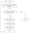
The DE algorithm is a parallel direct search algorithm that performs random operations on candidate populations. The steps are mainly to initialize the randomly selected population and initialize the parameters of the DE algorithm, and then determine whether the termination conditions are satisfied. At this point, if the termination condition is not satisfied, the mutation operation, crossover operation, and selection operation will be performed, followed by an iterative loop, and then the above steps will be performed once more until the termination condition is satisfied; the flow chart is shown in Fig. 1.
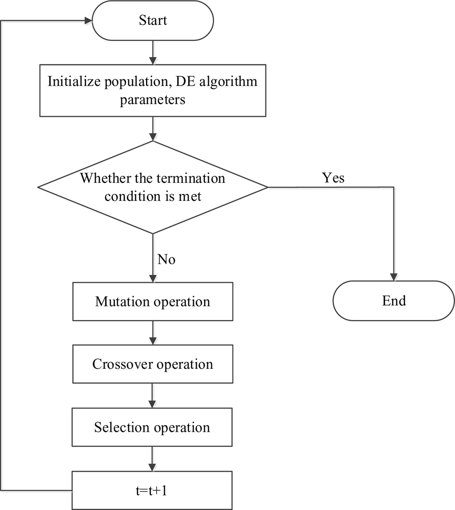
Figure 1: DE algorithm flow chart.
B. Application of the DE algorithm in CMC high frequency modeling
The DE algorithm is used for high frequency modeling of the CMC, in essence, the impedance measurement data of the CMC is processed using the DE algorithm to solve the relevant RLC parameters in its equivalent circuit in order to obtain the optimal solution of the above parameters. The specific steps of the DE algorithm to process the impedance data of CMC are as follows [21].
Step 1: Propose the equivalent circuit topology of the CMC and obtain the expressions of its CM and DM impedances.
In this paper this is the CM impedance expression Z and the DM impedance expression Z.
Step 2: Extraction of device impedance information.
The CMC equivalent circuit modeling based on the DE algorithm needs to solve the expression about the impedance Z derived from its equivalent circuit model according to the impedance information of the CMC, so as to obtain its optimal equivalent model RLC parameters.
Step 3: Optimal parameter problem transformation.
The impedance expression obtained from the CMC equivalent circuit topology is transformed into an expression for the impedance amplitude Z, and then Z is used as the original function of the RLC parameters to be optimized, and the measured impedance data Z is the sample. Let the expression of the CM or DM impedance Z of the CMC equivalent circuit model be:
| (1) |
where D is the spatial dimension, , and denote the maximum and minimum values of the jth component x, respectively, f is an independent variable, Z is a dependent variable, and x,x,x,…,x are the parameters to be determined, which are the RLC parameters of the CM (DM) impedance equivalent model in this paper. The DE algorithm is applied to the RLC parameter extraction of the CM (DM) equivalent impedance, and its optimization criterion function can be established by the least-square sum of the residuals of the system model as follows:
| (2) |
Step 4: Initialize the parameters.
For the initial populations randomly generated,
| (3) |
where N is the population size, x(0) refers to the ith individual of generation 0 in the overall population, and x(0) refers to the jth gene of the ith individual of generation 0. rand(0,1) denotes the number of random distributions between 0 and 1.
Step 5: Variation operation.
The DE algorithm takes the actual value parameter vector as the population of each generation and the weighted difference of two individuals in the population as the intermediate individual, i.e., the difference vector. The difference vector is then added to the third individual to generate mutations as follows:
| (4) |
where F is the mutagenic factor and x(g) is the ith individual of the g-generation population.
Step 6: Crossover operation.
The crossover operation refers to the exchange of some components of individuals in the current population with the corresponding components of mutant individuals according to certain rules to produce a crossover population. g-generation population |x(g)| and its variant v(g+1) are crossed over as follows:
| (5) |
where j is a random integer in [1,2,3,…,D] and C is the crossover probability.
Step 7: Selection operation.
If the objective function of the next generation individual is smaller than that of the current individual, the next generation individual will replace the current individual:
| (6) |
Step 8: Convergence discriminant operation.
Let the optimal individual in x(g + 1) be x(g + 1). The operation can be finished when DE runs to a predetermined number of times or the objective function value Q reaches the set accuracy, and the predicted result is the optimal value of RLC parameters. If there is no convergence, the operation returns to the second step and performs variation, crossover, and selection again.
III. CMC AND CAPACITOR HIGH FREQUENCY MODELING
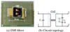
The physical and circuit topology of the EMI filter used in this paper is shown in Fig. 2, followed by modeling of the high frequency characteristics of the CMC, X capacitor and Y capacitor, respectively.
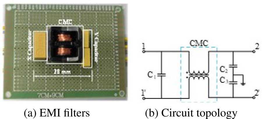
Figure 2: EMI filter physical and circuit topology.
A. CMC high frequency modeling
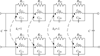
The equivalent model of the CMC is shown in Fig. 3. The model consists of multiple CM and DM resonant stages corresponding to resonances that may appear in the measured CMC impedance waveform, and also to improve high-frequency model accuracy. Each resonant stage consists of a pair of coupled inductors, where the coupling coefficient k = 1 between the upper and lower inductors of the resonant stage in the common mode part and k = 1 between the upper and lower inductors of the resonant stage in the differential mode part. The introduction of the mutual inductance factor ensures that, ideally, the differential mode path is shorted when the circuit flows common mode current and the common mode path is shorted when the differential mode current flows [20]. R and R represent the core resistance, reflecting the energy loss in the ferrite core due to hysteresis and eddy currents energy loss of the ferrite core; C and C represent the intra-winding capacitance; C is the inter-winding capacitance.
Since the two windings of the CMC are completely symmetrical in practice, to reduce CM EMI noise, an attempt is made to ensure that the line impedance where the two windings are located is balanced, so the effect of C on the CM path can be disregarded. Therefore, in the CM path, the CMC equivalent circuit can be viewed as a circuit with complete symmetry between the upper and lower components [19]. In the DM path, because C is tolerant when the frequency is very low, therefore, when performing data fitting, the value of C is only obtained from the starting frequency point to the first valley frequency range of the measured impedance value, and the value of other frequency bands is the same.
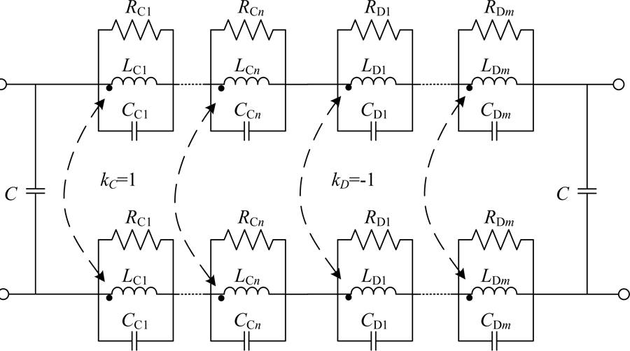
Figure 3: CMC high frequency equivalent circuit.
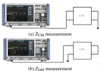
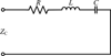
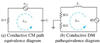
After determining the circuit topology of the CMC, the next step is to measure the impedance of the CMC. In this paper, we use a VNA to measure the impedance of CMC. When measuring the CM impedance of the CM path Z, ports 1 and 2 are shorted and then connected to the VNA, as shown in Fig. 4 (a), the expression of the CM path impedance relative to it is
| (7) |
When measuring the DM impedance Z of the DM path, the two ports of the CMC are short-circuited, as shown in Fig. 4 (b), and the expression of the differential mode path impedance relative to it is
| (8) |
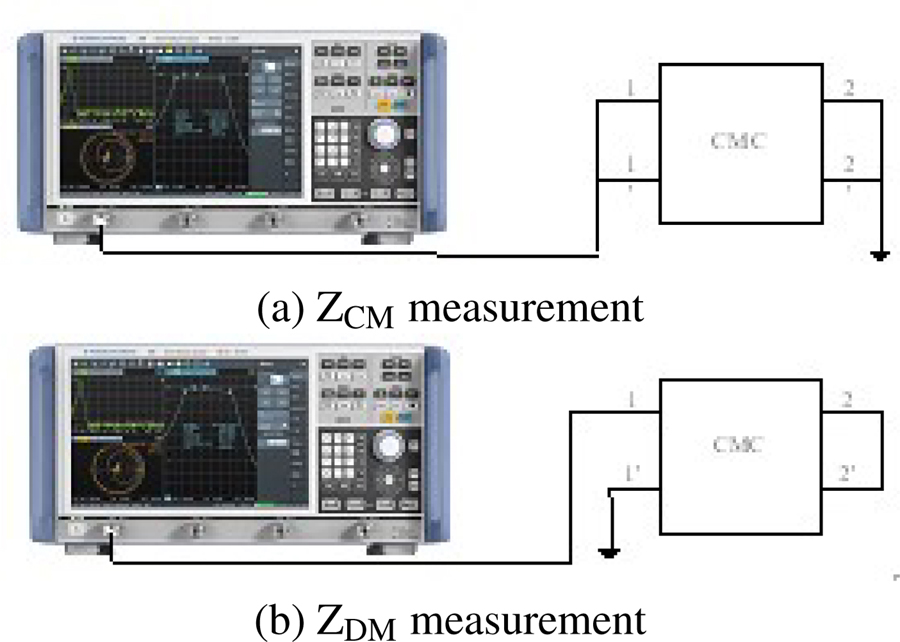
Figure 4: CMC impedance measurement.
In order to obtain high accuracy RLC values on a computer with limited performance for high frequency modeling of CMC, this paper uses a segmented fitting method to process the measured impedance data, i.e., the first segment from the start frequency to the first trough of the impedance waveform, the second segment from the first trough to the second trough, and so on. In this method, even if a professional workstation computer is not used, a personal computer can be used to process the measured impedance data and obtain the RLC values with high accuracy.
The fitting process of the common-mode impedance can be seen from the description of the application of the DE algorithm in the high-frequency modeling above. We have completed the first and second steps, and then replaced Eq. (1) with Eq. (7), and the measured impedance data is the sample Z. We then wait for the algorithm to run and then extract the RLC value from the common-mode impedance data. The same is true for the fitting of the differential mode impedance, but it should be noted that the intergroup capacitance C comes from the first frequency band. Therefore, we use the DE algorithm and Eq. (8) to extract the value of RLC and the value of the inter-winding capacitance C in the first frequency band. In the frequency bands other than the first frequency band, we substitute the value of the inter-group capacitance C into Eq. (8), and then use the newly obtained formula to extract the value of the RLC of the remaining frequency segments.
Table 1: RLC values of CMC CM and DM
| CM | i = 1 | i = 2 | DM | i = 1 | i = 2 |
| R | 19.9 k | 0.16 k | R | 17.4 k | 0.42 k |
| L | 0.19 mH | 8.77 nH | L | 7.67 H | 4.46 nH |
| C | 7.20 pF | 19.60 pF | C | 2.39 pF | 41.8 pF |
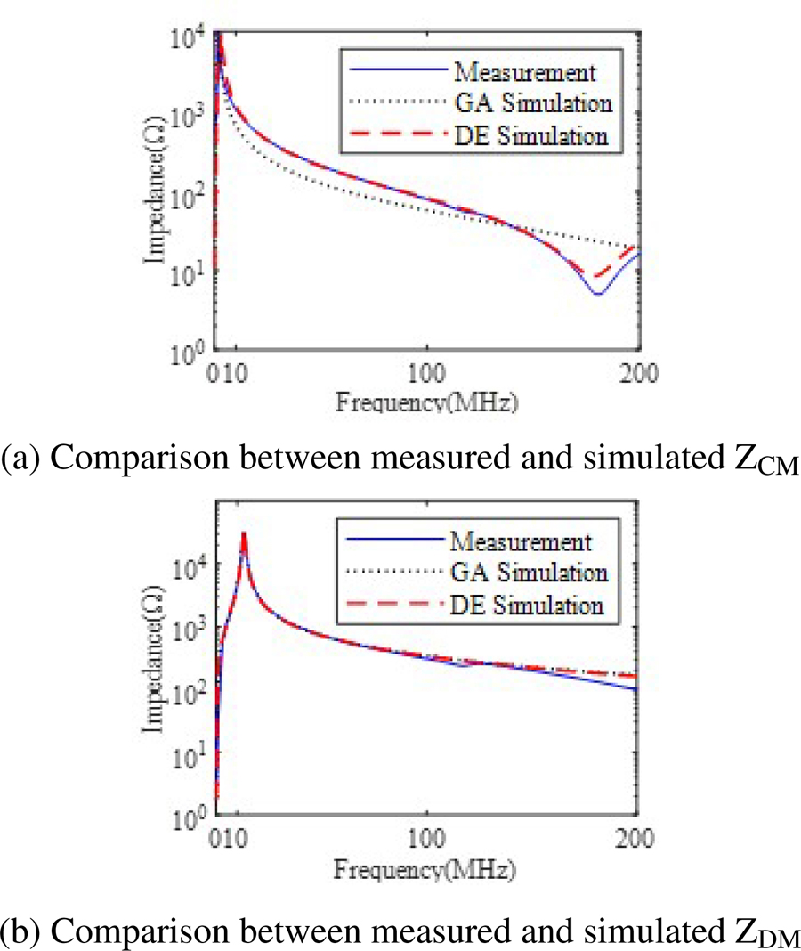
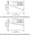
Figure 5: Comparison between simulation and measurement of the CMC impedance waveform.
The values of RLC extracted by the DE algorithm are shown in Table 1, while the parasitic capacitance between windings C = 3.56 pF. A comparison of the simulated and measured CMC CM and DM impedance waveforms based on the GA and DE algorithms, respectively, is shown in Fig. 5. It can be seen from Fig. 5 that, in the low frequency band, the CM impedance and DM impedance curves of the CMC tend to match the measured ones regardless of the algorithm. In the high frequency section, the simulated and measured impedance curves show that the DE algorithm has better accuracy than the GA algorithm for the high frequency model in the CM path.
The reason for such different results is that although both the DE algorithm and the GA algorithm randomly generate the initial population, the fitness value of each individual in the population is the selection criterion, and the main process also includes three steps of mutation, crossover and selection. However, the GA algorithm is based on the fitness value to control the crossing of the parent generation. The probability value of the offspring generated after the mutation is selected. In the maximization problem, the individual with a large fitness value has a correspondingly higher probability of being selected. The DE algorithm mutation vector is generated by the difference vector of the parent generation, and crosses with the individual vector of the parent generation to generate a new individual vector, which is directly selected by means of the individual of the parent generation. Therefore, the approximation effect of the differential evolution algorithm is more significant than that of the genetic algorithm, which also makes the model established using the DE algorithm more accurate than the GA algorithm in this paper.
B. High frequency modeling of capacitors
After the high-frequency characteristic modeling of the CMC is completed, the high-frequency characteristic modeling of the capacitor is carried out next. The X capacitance values used in this paper are C= 4.7 F and Y capacitance C= C= 2200 pF. The high-frequency equivalent model of the capacitor is shown inFig. 6.
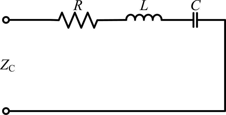
Figure 6: High frequency model of capacitance.
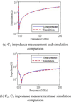
The following is the same as the CMC high-frequency modeling method. First, the impedance data of the capacitor at different frequencies are measured using the VNA. Then, impedance data is processed using the DE algorithm. Finally, the RLC value of the high-frequency equivalent model of the capacitor is shown in Table 2, and the impedance comparison between measured and simulated data is shown in Fig. 7. It can be seen from Fig. 7 that, regardless of high frequency or low frequency, the DE algorithm can extract the relevant parameters of the capacitor very well.
Table 2: Capacitor high frequency equivalent model RLC
| C | C, C | |
|---|---|---|
| R | 0.19 | 0.18 |
| L | 26.2 nH | 28.3 nH |
| C | 0.48 uF | 2.85 nF |
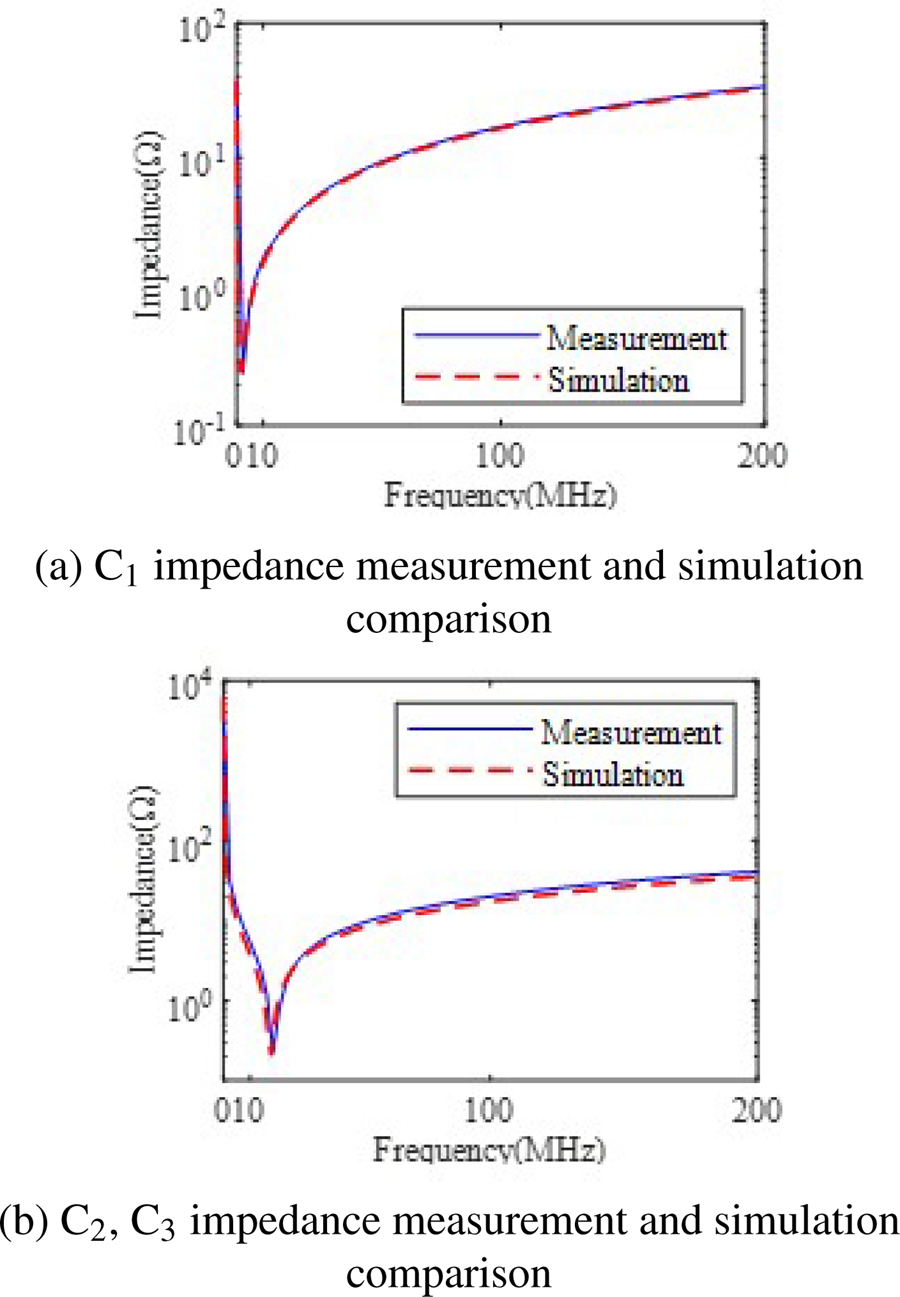
Figure 7: Comparison of the capacitive impedance simulation and actual measurement.
IV. CMC CONDUCTED INTERFERENCE SUPPRESSION ANALYSIS
In the above we have finalized the EMI filter components of the high-frequency model, according to its topology, in order to assemble the EMI filter to complete the establishment of a high-frequency model. In order to analyze the suppression effect of the high-frequency equivalent model of the EMI filter on the conduction interference, this paper selects a switching power supply with an output of 24 V/2 A, 48 W to do the actual measurement and comparison of the interference. The switching power supply is a Boost PFC circuit, and the two diodes of the rectifier bridge are forward-biased conducting; the interference propagation path is shown in Fig. 8 [22], in which MOSFET Q is the main noise source.
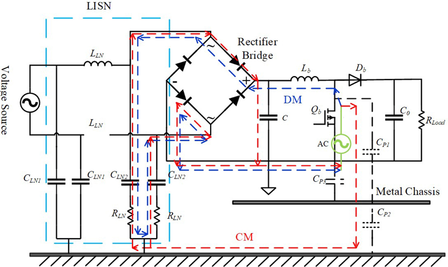
Figure 8: Boost PFC circuit interference propagation path.
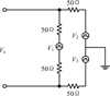
In the analysis of the conducted interference, in order to simplify the analysis, in the CM path when only the MOSFET drain voltage V as a CM conducted interference noise source, the line impedance stabilization network (LISN) structure is simplified to two 50 parallel test impedances in a simplified circuit, as shown in Fig. 9 (a). DM interference is caused by high-frequency interference currents in the loop, while the PFC circuit DM conducted EMI interference is usually considered to be caused by the ripple of the inductor current i. This current is the DM current driven by the MOSFET drain voltage V along the loop, as shown in Fig. 8, this loop consists mainly of a MOSFET, a rectifier bridge, and a LISN test resistor. For the differential mode current, the series connection of the L and N two-wire test impedance of the LISN can be equivalent to a 100 resistance, as shown in Fig. 9 (b).
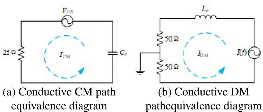
Figure 9: Conducted interference path equivalence diagram.
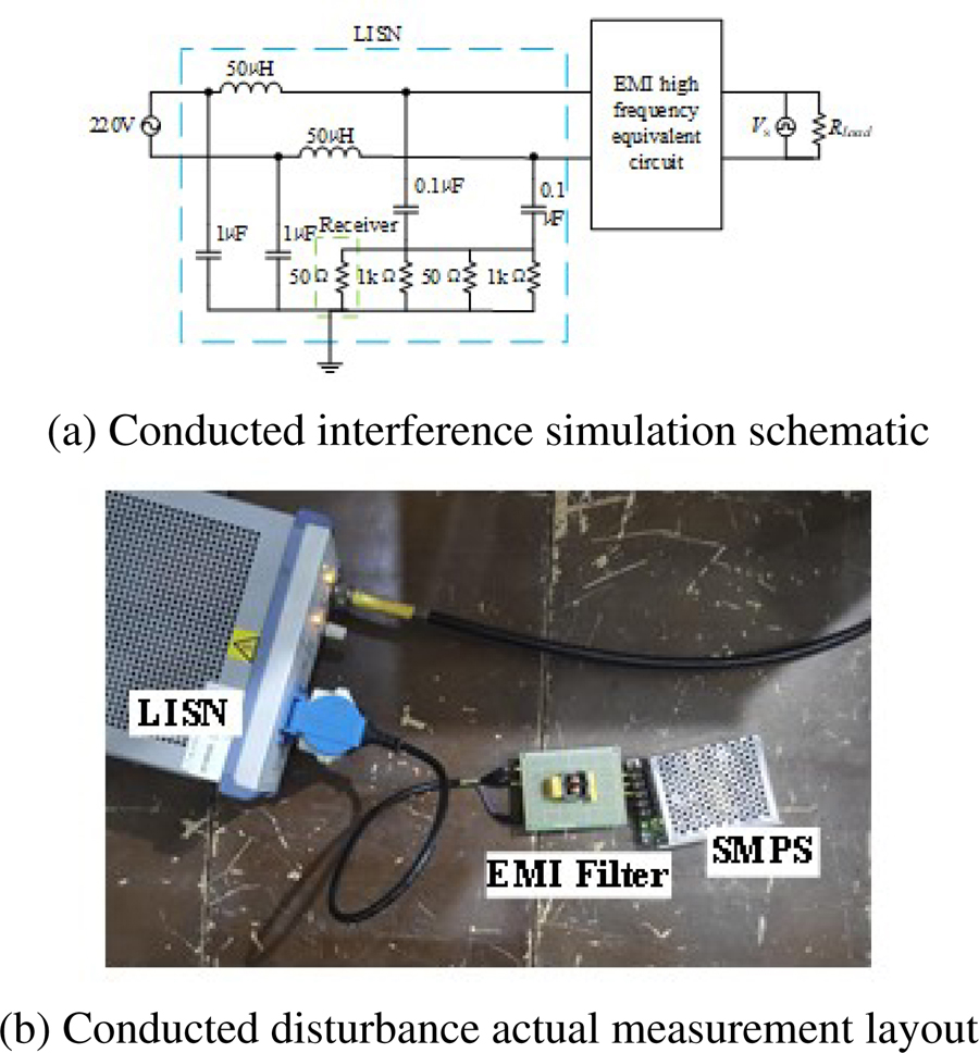
Figure 10: Conducted interference noise simulation and actual measurement chart.
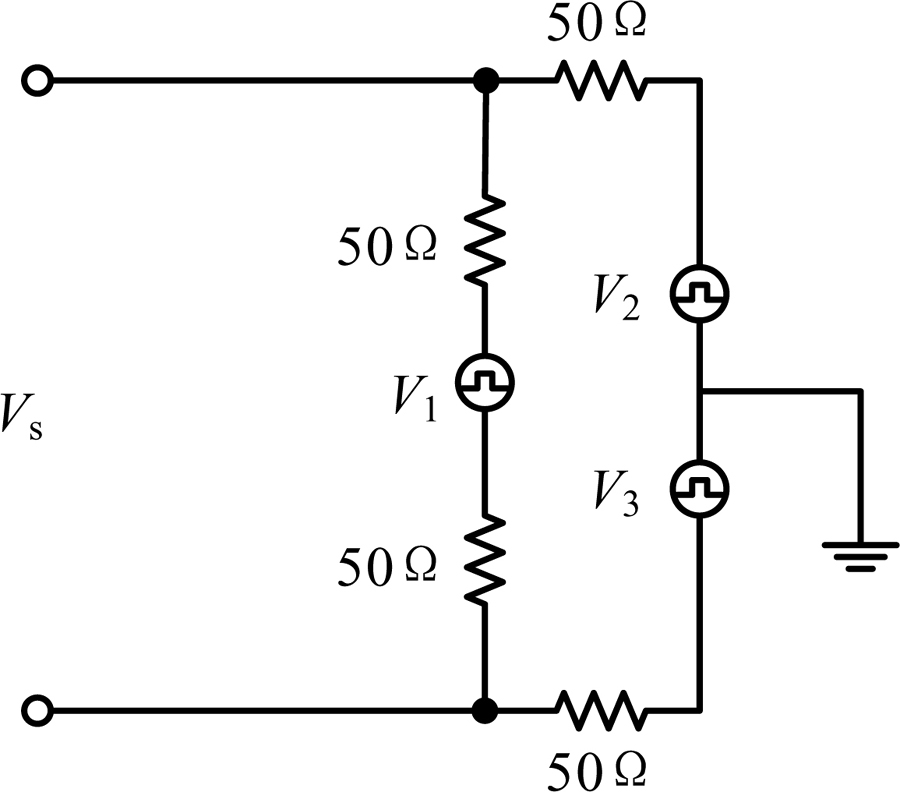
Figure 11: Interference source circuit topology.
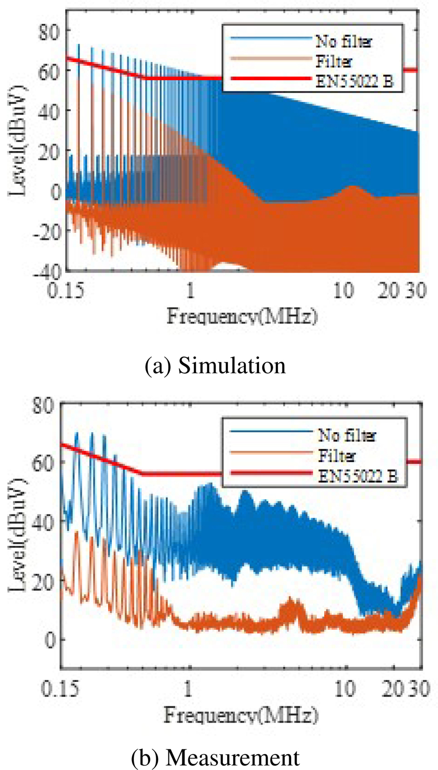
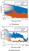
Figure 12: Conducted interference noise waveform diagram.
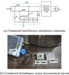
In this paper, because the high-frequency model of the CMC introduced the mutual inductance coefficient, the conducted interference simulation does not have to be divided into CM and DM paths. In the conducted interference simulation modeling, the output of a square wave voltage source is a noise source, so as to verify the EMI high-frequency model of the conducted interference noise suppression capability. The conducted interference simulation is built in PSpice, a simulation schematic of which is shown in Fig. 10 (a). The V consists of a square wave voltage source with a frequency of 20 kHz, a voltage of 0.05 V and a resistor of 50 . The circuit topology is shown in Fig. 11. V is a DM interference source, V and V together form a CM interference source to simulate the noise source of the conducted EMI generated by the boost circuit during operation. The conducted interference noise test apparatus of the switching power supply is arranged as shown in Fig. 10 (b). Simulation of the conducted interference waveform, as well as the EMI filter to suppress the interference waveform, is shown in Fig. 12 (a); measured with and without EMI filter conducted interference waveform. The results are shown in Fig. 12 (b).
From Fig. 12, it can be found that the EMI filter in the real test has a good suppression of conducted interference, and the EMI filter high-frequency equivalent model also reflects this suppression ability. Since the noise source in the simulation is ideal and only simulates the switching frequency in the actual operation of the switching power supply, it does not fully reflect the real noise of the switching power supply used in the actual test. However, by comparing the measured and simulated, EMI filter suppression of the conducted interference can be found. The EMI filter high-frequency model can reflect the conductive interference suppression ability of the filter, but also proves that the modeling method of this paper works.
V. CONCLUSION
This paper proposes a method for modeling the CMC high frequency model in the frequency range from 9 kHz to 200 MHz. The method only requires measuring the CM and DM impedance data and extracting the RLC value from the impedance data by using the DE algorithm in separate frequency bands to complete the CMC high frequency modeling. Then, based on the built CMC high-frequency model, a high-frequency model of the EMI filter is further established. This high-frequency model does not need to be divided into CM and DM channels when performing conduction interference simulation. Finally, the EMI filter high frequency equivalent model is used to build a simulation test model of conducted interference noise, which verifies the suppression capability of the CMC high-frequency equivalent model for conducted interference noise and radiated interference noise.
In addition, this modeling method adopts the fitting method of sub-frequency bands, so the establishment of high-frequency models can be completed on personal computers without professional workstations. The use of the DE algorithm in extracting the RLC value in the impedance data can complete the establishment of the CMC high-frequency model in the frequency range 9 kHz to 200 MHz while maintaining high accuracy. In addition, because the high-frequency model of the EMI filter in the frequency range 9 kHz to 200 MHz can be obtained by using this modeling method, the model can also provide a reference for the radiation interference suppression of the switching power supply.
ACKNOWLEDGMENT
This paper is supported by National Natural Science Foundation of China (52107005).
REFERENCES
[1] C. R. Paul, Introduction to Electromagnetic Compatibility, 2nd edn., John Wiley & Sons, New York, pp. 414-426, 2005.
[2] H. Chen, Y. Hu, and L. Wang, “EMI filter design based on high-frequency modeling of common-mode chokes,” IEEE 27th International Symposium on Industrial Electronics (ISIE), pp. 384-388, 2018.
[3] H. Hemphill and B. Wallertz, “Critical core parameters in the design of common mode suppression chokes,” International Conference on Electromagnetic Interference and Compatibility (INCEMIC), pp. 334-336, 1995.
[4] Z. Li, D. Pommerenke, and Y. Shimoshio, “Common-mode and differential-mode analysis of common-mode chokes,” IEEE Symposium on Electromagnetic Compatibility. Symposium Record (Cat. No.03CH37446), vol. 1, pp. 384-387, 2003.
[5] W. Shen, F. Wang, D. Boroyevich, V. Stefanovic, and M. Arpilliere, “Optimizing EMI filter design for motor drives considering filter component high-frequency characteristics and noise source impedance,” Nineteenth Annual IEEE Applied Power Electronics Conference and Exposition, vol. 2, pp. 669-674, 2004.
[6] J. R. Regue, M. Ribo, D. Duran, D. Badia, and A. Perez, “Common and differential mode characterization of EMI power-line filters from S-parameters measurements,” International Symposium on Electromagnetic Compatibility (IEEE Cat. No.04CH37559), vol. 2, pp. 610-615, 2004.
[7] A. Roc’h and F. Leferink, “In situ performances of common mode chokes,” 10th International Symposium on Electromagnetic Compatibility, pp. 494-499, 2011.
[8] H. Chen and Z. Qian, “Modeling and characterization of parasitic inductive coupling effects on differential-mode EMI performance of a boost converter,” IEEE Transactions on Electromagnetic Compatibility, vol. 53, pp. 1072-1080, 2011.
[9] J. Kotny, X. Margueron, and N. Idir, “High-frequency model of the coupled inductors used in EMI filters,” IEEE Transactions on Power Electronics, vol. 27, pp. 2805-2812, 2012.
[10] W. Tan, C. Cuellar, X. Margueron, and N. Idir, “A high frequency equivalent circuit and parameter extraction procedure for common mode choke in the EMI filter,” IEEE Transactions on Power Electronics, vol. 28, pp. 1157-1166, 2013.
[11] A. Asmanis, G. Asmanis, D. Stepins, and L. Ribicks, “High-frequency modelling of EMI filters considering parasitic mutual couplings,” ESA Workshop on Aerospace EMC (Aerospace EMC), pp. 1-6, 2016.
[12] F. Hami, H. Boulzazen, and M. Kadi, “High-frequency characterization and modeling of EMI filters under temperature variations,” IEEE Transactions on Electromagnetic Compatibility, vol. 59, pp. 1906-1915, 2017.
[13] D. Xu, C. K. Lee, S. Kiratipongvoot, and W. M. Ng, “An active EMI choke for both common- and differential-mode noise suppression,” IEEE Transactions on Industrial Electronics, vol. 65, pp. 4640-4649, 2018.
[14] C. Dominguez-Palacios, J. Bernal, and M. M. Prats, “Characterization of common mode chokes at high frequencies with simple measurements,” IEEE Transactions on Power Electronics, vol. 33, pp. 3975-3987, 2018.
[15] H. Chen, J. Wu, and X. Zheng, “Elimination of common-mode choke saturation caused by self-resonance of the EMI filter in a variable-frequency drive system,” IEEE Transactions on Electromagnetic Compatibility, vol. 61, pp. 1226-1233,2019.
[16] C. Dominguez-Palacios, P. Gonzalez-Vizuete, M. A. Martin-Prats, and J. B. Mendez, “Smart shielding techniques for common mode chokes in EMI filters,” IEEE Transactions on Electromagnetic Compatibility, vol. 61, pp. 1329-1336,2019.
[17] R. He, Y. Xu, S. Walunj, S. Yong, V. Khilkevich, D. Pommerenke, H. L. Aichele, M. Boettcher, P. Hillenbrand, and A. Klaedtke, “Modeling strategy for EMI filters,” IEEE Transactions on Electromagnetic Compatibility, pp. 1-10, 2020.
[18] D. Liu and X. Jiang, “High frequency model of common mode inductor for EMI analysis based on measurements,” 3rd International Symposium on Electromagnetic Compatibility, pp. 462-465, 2002.
[19] H. Chen, High-frequency Modeling of EMI Filter: Research on Parasitic Effect, Zhejiang University, pp. 26-37, 2007.
[20] I. Stevanovic, S. Skibin, M. Masti, and M. Laitinen, “Behavioral modeling of chokes for EMI simulations in power electronics,” IEEE Transactions on Power Electronics, vol. 28, no. 2, pp. 695-705, 2013.
[21] C.-L. Li, C.-H. Huang, C.-C. Chiu, and C.-H. Sun, “Comparison of dynamic differential evolution and asynchronous particle swarm optimization for inverse scattering of a two-dimensional perfectly conducting cylinder,” Applied Computation Electromagnetics Society (ACES) Journal, vol. 27, no. 10, pp. 850-865, 2021.
[22] C. Y. Wu, H. Kim, J. Y. He, N. Erickson, S. Cho, D. Kim, Y. Hur, D. J. Pommerenke, and J. Fan, “Analysis and modeling of conducted EMI from an AC-DC power supply in LED TV up to 1 MHz,” IEEE Transactions on Electromagnetic Compatibility, vol. 61, pp. 2050-2059, 2019.
BIOGRAPHIES

Yakang Pei was born in China. He completed his studies in Electrical Engineering and its Automation at the Haibin College of Beijing Jiaotong University in Cangzhou, Hebei, China in 2019, and received his bachelor’s degree in Engineering. He is a master student at Nanjing Normal University with research interests in electromagnetic compatibility and high frequency device modeling.
Wei Yan is an Associate Professor at Nanjing Normal University. He obtained his Physics and Electronics Ph.D. and Electrical Engineering M.Sc. from Nanjing Normal University in 2014 and 2011. He is the Senior Member of China Electrical Technology Association and the evaluation expert of the Electromagnetic Compatibility Calibration Specification of China.

Hao Ma was born in Yangzhou, China. He received his B.Sc. degree in Automation from Jiangsu Normal University, Xuzhou, China, in 2019. He is currently working in electromagnetic compatibility of power supply system with Nanjing Normal University. His research interests are in the areas of Electromagnetic Compatibility and Power Electronics.
Mengxia Zhou received his M.Sc. degree in Electrical Engineering and his Ph.D. degree in Physics and Electronics from Nanjing Normal University, in 2018 and 2021, respectively. His main research interests include electromagnetic compatibility, electromagnetic environment effects, and high frequency device modeling.

Yang Jian was born in China. In 2021, he graduated from Jiangsu Institute of Technology, Changzhou, Jiangsu Province, China, majoring in Electrical Engineering and automation, with a Bachelor of Engineering degree. He is a Master’s student at Nanjing Normal University, majoring in electromagnetic compatibility.
ACES JOURNAL, Vol. 38, No. 2, 91–99
doi: 10.13052/2023.ACES.J.380203
© 2023 River Publishers