Ultra-wideband Terahertz Absorber Based on E Shape Graphene Pattern
Muhammad Sajjad, Xiangkun Kong, Shaobin Liu, Saeed Ur Rahman, Zakir Khan, and Owais
1Key Laboratory of Radar Imaging and Microwave Photonics
Ministry of Education, College of Electronic and Information Engineering
Nanjing University of Aeronautics and Astronautics (NUAA), Nanjing, 211106, China
sajjadwazir@nuaa.edu.cn, xkkong@nuaa.edu.cn, lsb@nuaa.edu.cn
2School of Electronic Engineering
Xidian University, Xi’an, China
saeed@xidian.edu.cn
3Department Micro-/Nano-Electronic System Integration Center
University of Science and Technology of China, Hefei 230027, China
zakirkhan@mail.ustc.edu.cn
4Department of Electrical and Computer Engineering
COMSATS University Islamabad, Abbottabad, 22060, Pakistan
mkowais@cuiatd.edu.pk
Submitted On: October 13, 2022; Accepted On: January 24, 2023
ABSTRACT
We present a tunable ultra-wideband (UWB) absorber based on a multilayer of “E” shaped graphene patterns. The numerically calculated results indicate that the absorption of the proposed design is above 95% in the range of 1.12 to 14.04 THz. By using the multiple layers of graphene, the relative bandwidth is 95% and reaches up to 170% of the central frequency. Furthermore, for transverse electric polarization mode at a resonating frequency of 1.68, 3.99, 7.51, 13.56, and 17.74 THz the absolute value exceeds 99.57, 99.37, 99.94, 99.86, and 99.09%, respectively. Also, owing to the structure’s rotational symmetry, the absorber is insensitive to both transverse magnetic (TM) and transverse electric (TE) polarization. The absorption peaks and frequency band can be controlled effectively by altering the Fermi level of graphene without modifying the structure manually. Moreover, the absorber exhibits steady absorption over an incident angle of 0 to 60, with just a minor decrease in bandwidth around 60.
Index Terms: absorber, broadband, graphene, tunable.
I. INTRODUCTION
In recent years, the research interest toward terahertz (THz) (0.1-10) frequency has increased due to its great potential in the areas of modulators, security, medical imaging spectroscopy, and communication [1, 2]. The THz absorber is a vital section that can be considered to be the practical application in the fields discussed above [3, 4]. However, it is very difficult to distinguish THz electromagnetic waves through a natural element. To resolve this problem, recently an artificial electromagnetic material known as metamaterial absorber (MMA) has been proposed which shows some remarkable electronic and optical properties. Graphene is a newly discovered 2-D monolayer based on a carbon atom. It has been widely considered in view of its unique electrical and optical properties [5, 6]. Its most desirable characteristics are that the conductivity and permittivity of the graphene can be dynamically controlled, by adjusting the Fermi level by external bias voltage or chemical doping, to obtain dynamically tunable MMAs [7, 8]. Over the last decade, numerous graphene-based tunable devices have been introduced which include transistors [9-12] and polarization convertors [13, 14]. A large number of graphene-based THz MMAs with different structures have been designed and published, including square patches [15], disks and ribbons [16], stacks [17], cross-shaped arrays [18], and as well as the combination of graphene wire and gold cut wire [19] configurations.
However, in the scope of our knowledge, the majority of these MMAs still have certain disadvantages, including single or narrow band absorption, and limited tunable range and considerable polarization and incident angle dependency, and having complex structure designs, thus reducing their potential application. In this article the “E” shape structure is designed as a basic absorber unit cell that is simple and reliable. It is found that an “E” shape has many resonance modes, which compete with each other and increase the frequency range. Additionally, the absorption is very consistent across a wide range of incident angles. The design method provides a new way of achieving the band, enhanced by using the C-4 symmetry of “E” shape graphene in multilayer. Due to C-4 symmetry, the proposed design is less sensitive to the incident angles.
We developed an ultra-wideband absorber with an absorption of more than 175% for the central frequency of 7.83 THz, which is considerably greater than the best previous work. To achieve wide bandwidth, multiple layers of “E” shaped graphene patterns are used. The calculated results indicate that absorption spectra greater than 90% from 0.97 to 14.70 THz has been achieved. An “E” shaped graphene pattern was evaluated numerically and results revealed that the efficiency and bandwidth of the absorber can be improved by using multiple layers of graphene, while also achieving dynamic tuning. Additionally, field distribution is examined in order to investigate the absorption mechanisms. Also, in order to minimize the reflection coefficient, the impedance of the designed device is adjusted to be approximately matched to the free-space impedance, further explained in the Results & Discussion section (III).
II. DESIGN AND SIMULATION
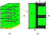
Figure 1 schematically show the structure of the suggested proposed ultra-wideband THz absorber. The proposed design consists of four layers of graphene in the “E” shape format. As shown in Fig. 1, all the four layers have the same structure but with 90 rotation. The graphene layers were deposited on silicon dioxide layers. The Topas layer with permittivity of 1.53 is considered as a low loss substrate [20]. Gold is selected as a ground metal as described by the Drude model [21].
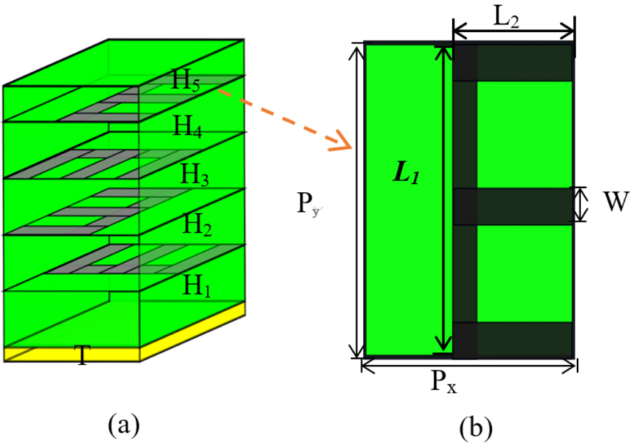
Figure 1: (a) Schematic diagram of the proposed UWB-MMA unit cell, (b) top view of the “E” shape graphene layer.
The other parameters are as follows: w=5 m, L=40 m, L=20 m, H=8 m, H=5 m, H=5 m, H=5 m, H=1 m and tm=0.1 m. The measurement along the x and y direction is 40 m. To determine the chemical potential of the ultra-wideband (UWB) absorber’s first layer, such as the graphene Fermi velocity, the electron mobility of the graphene and the relaxation time can be calculated as follows. If we set [22]. , [24] and the chemical potential can be adjusted to 0.97 eV. The suggested design was numerically investigated by applying the frequency domain approach using commercial CST microwave studio simulation tools. The conductivity of graphene is composed of two parts, namely intraband and interband electron transition derived from the Kobo formula () [25]. In the THz and mid-infrared (MIR) wavelength ranges, the graphene intraband contribution is dominant because . So, in the view of the Puli exclusion principle for the THz frequency domain () at room temperature, the above expression is further simplified to the Drude model [26]:
| (1a) |
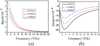
where represents reduced planks constant, e, , and are electron charge, the relaxation time and angular frequency of the incident wave, respectively. The conductivity of the graphene at various Fermi levels is determined in Figs. 2 (a) and (b). When the Fermi level is fixed, it is shown that the real and imaginary parts of conductivity are proportional to the frequency. The amplitude modulation of the resonance is determined by the real component of the conductivity, while the resonance’s spectral shift is controlled by the imaginary portion of the conductivity [27-29].
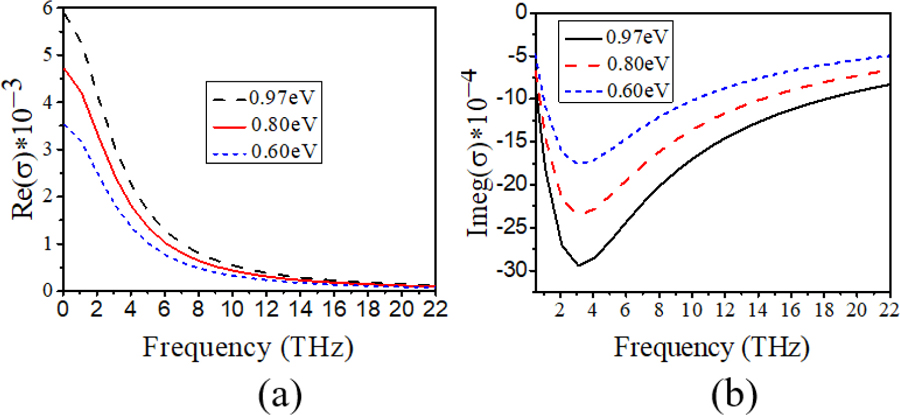
Figure 2: Surface conductivity of the graphene with different chemical potential (a) Real part. (b) Imaginary part.
The theoretical relationship between and can be expressed as [30, 31]:
| (1b) |
where, the Fermi velocity and external bias voltage are and . The permittivity of substrate and vacuum is denoted by and . Equation [1b] indicates that carrier density can be modified by voltage or chemical doping due to the presence of the carrier density. By changing the bias voltage, graphene conductivity can be adjusted. The equivalent relative permittivity is then derived from the surface conductivity as follows [32]:
| (1c) |
where represents graphene surface conductivity, and t are vacuum permittivity and the thickness of the graphene layer. In equation (1c), the permittivity of the graphene can be found by measuring the conductivity of the graphene surface. The conductivity of the graphene surface can also be found by measuring the applied voltage. Thus, equations (1a-1c) show that the applied voltage may dynamically change the electromagnetic properties of graphene, implying that the structure absorption characteristics can likewise be dynamically adjusted. As a result, the absorbance may be varied by adjusting the Fermi level through applied voltage. The periodic boundary condition in the x-y plane is set in simulations and the incident THz wave will travel in the Z-direction as depicted in Fig. 1. Naturally, single-layer designs are simpler to produce than multilayer designs, but the use of multilayering is needed to enable high absorption rates and adjustable performance. The absorbance of the proposed design is computed/calculated as A=1-T-R=1-|S(w)|-|S(w)|, where T=|S(w)| and R=|S(w)|, represent transmittance and reflectance respectively. The thickness of the gold ground is 0.5 m, which is significantly higher than the skin depth, allowing S to be technically reduced to zero.
III. RESULT AND DISCUSSION
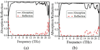
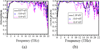
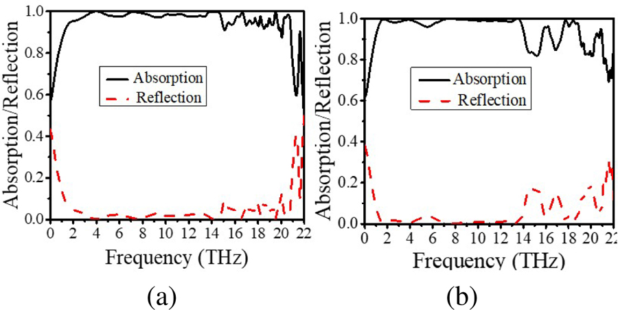
Firstly, to elevate the absorption efficiency of the proposed UWB-MMA. The unit cells are simulated under a normal THz incident wave. The calculated result is shown in Fig. 3. The TM incident wave is shown in Fig. 3 (a). The proposed UWB-MMA has a simulated reflective spectrum below 0.3 for 0.50 to 14.50 THz and has an absorption spectrum of more than 95% in the same range, as shown in Fig. 3 (a). For the TE incident wave the reflective spectrum is below 0.3 for 0.50 to 21.20 THz band, while the associated absorption is also higher than 95% within the 12.92 THz bandwidth as shown in Fig. 3 (b). The TM resonant frequencies in five distinct bands 3.94, 7.17, 14.05, 16.63, and 19.53 THz have 99.95, 99.65, 99.85, 99.54, and 99.70%, respectively, of the absorption spectrum.
These findings illustrate the almost symmetric pattern of the TM and TE polarization waves due to the almost symmetric structure of UWB-MMA as shown in Fig. 1. Furthermore, for TE polarization mode at resonating frequencies of 1.68, 3.99, 7.51, 13.56, and 17.74 THz the absolute value exceeds 99.57, 99.37, 99.94, 99.86, and 99.09%, respectively.
(a) (b)
Figure 3: Absorption and reflection spectra of the proposed UWB-MMA (a) TM mode. (b) TE mode.
The characteristics of the complete absorption could be described using impedance matching theory. The absorber’s effective impedance maybe represented as [33]:
| (1) |
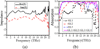
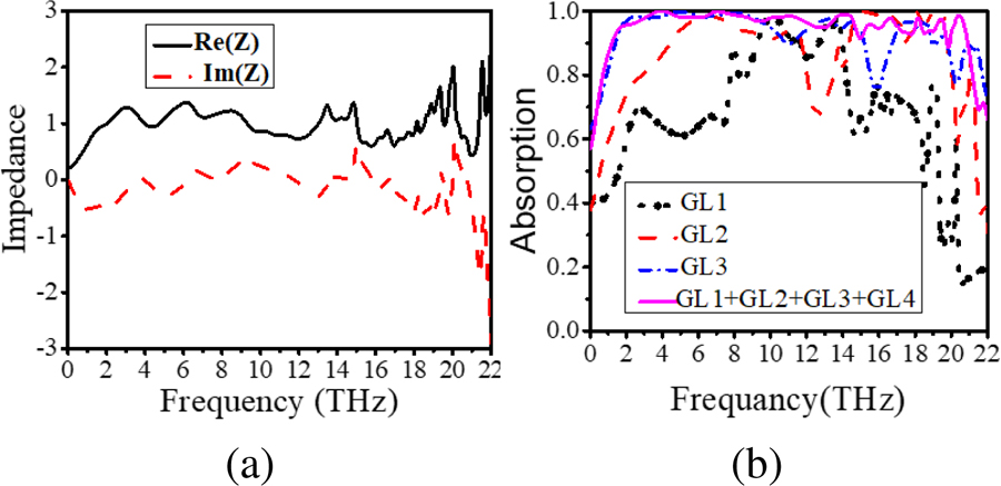
where and represent the effective permeability and permittivity, correspondingly. The S parameter is used to calculate the real and imaginary components of the impedance. If the device effective impedance approaches that of free space, significantly high absorption can be obtained. As shown in Fig. 4 (a), at a broad bandwidth the real component is near to 1 and imaginary part is close to 0, demonstrating that the effective impedance of the proposed device has equaled that of free space. This indicates that the absorber impedance steadily approaches that of empty space, which is characteristic of perfect absorber [34].
(a)(b)
Figure 4: The relative input impedance and absorption spectrum of the proposed UWB-MMA, (a) input impedance (b) absorption spectrum.
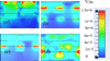
To describe the strong absorption in ultra-wideband bandwidth, the absorption spectrum is determined for each layer separately. When contrasting the effects of individual graphene layers with the whole system, the peaks of the whole system at 3.9, 4.6, 14.8, and 13.7 THz frequency band are led, respectively, by the fourth, third, second, and first layer, as shown in Fig. 4 (b). The UWB of the absorber is closely linked to each of these four peaks. The simulated field distribution demonstrated that UWB absorption of the proposed design can be considered as a superposition of these graphene layers. Absorption peaks at varying frequencies are close together and superimposed for UWB absorption. Then, to further explain the physical mechanism behind the UWB near-perfect absorption, we also provide a comprehensive analysis of electric field amplitude distributions at various frequencies under the setting of the Fermi level to 0.97 eV. Figure 5 illustrate electric field distributions of the unite cell at four distinct frequency bands under normal incidence TE wave. It may be noted that, as shown in Fig. 5, the suggested structure exhibited strong electric field confinement between the different layers of graphene and dielectric, leading to high absorption. This is the basic characteristic of the localized surface plasmonic. As depicted in Fig. 5 (a), from the simulated field distribution, it is evaluated that UWB absorption is achieved by the superposition of these graphene layers. As depicted in Fig. 5 (a), the top layer is largely attributed to the absorption peak around 3.9 THz. While the absorption peak at 4.6, 14.8, and 13.7 THz is primarily due to the third, second and first graphene layer respectively. Absorption peaks of various frequencies are closer to each other and superimpose to form an UWB absorption.
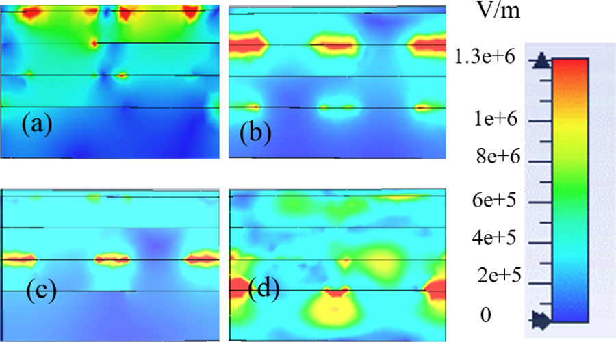
Figure 5: Electric field distribution in TE polarization at XOZ plan at (a) 3.9 THz, (b) 4.6 THz, (c) 14.8 THz, and (d) 13.7 THz.
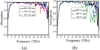
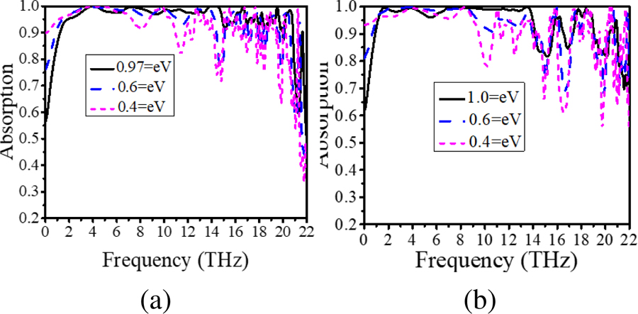
The absorption band is changed accordingly because graphene permittivity could be regulated by the chemical potential. The absorption changes to higher frequencies with increasing bandwidth and magnitude, as a result of increasing Fermi level. Figure 6 illustrate how the graphene Fermi level regulates the absorption spectrum with constant W and T. If the Fermi level increases, the graphene surface plasmon resonance increases and the structure absorption is higher with the E =0.97 eV absorption band from 0.90 to 14.40 THz exceeds 90%. We have also investigated the influence of the permittivity and thickness of the substrate on the absorption property of the unit cell.
(a)(b)
Figure 6: The absorption spectra of the proposed UWB-MMA under different Fermi levels (a) TM waves. (b) TE waves.
Figure 7 illustrate the influence of the dielectric thickness of the first and fifth layers (H and H) over the absorption curve of the proposed absorber. When increasing the dielectric thickness value, the resonating frequencies are red-shifted. The high-frequency absorption curve shift to the left occurs, while the low-frequency band almost remains constant. When H and H are more than 8 m and 1 m the absorption rate at the center of the absorption band is less than 90%. The resonant coupling between the top and bottom layers of the graphene relies to a significant degree on their distance from one another. By increasing or reducing the coupling distance, near field coupling is reduced to a certain degree, resulting in a variation in absorption performance. Table 1 shows a comparison of our work with previously published works.

(a)(b)
Figure 7: Absorption curve of the proposed absorber with different thicknesses of dielectric layer (a) first layer, and (b) fifth layer.
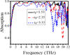
As shown in Fig. 8, the absorption spectrum’s reliance on the dielectric substance is investigated in detail. The structure’s whole set of parameters is stable and unaltered, and only the permittivity of the substrate is changed. As the permittivity decreased from 3.35 to 1.53, a minor change in the amplitude of absorption occurs while frequency shifts to the right.
Equation (3) shows the influence of the frequency shifts on the thickness and permittivity of the substrate. The and will be constant, as the plan wave will be transmitted on the homogenous medium layer at normal incidence.
Table 1: Performance comparison of the graphene bases UWB absorber with published work
| Ref. | Absorption Bandwidth (THz) | F(THz) | Thickness (m) | Angle | Fractional Bandwidth (%) | Absorptivity |
| [35] | 2.04-0.83 =1.21 | 1.435 | 0.07 | 0-50 | 84.3 | 90% |
| [36] | 7.85-2.05= 5.8 | 4.94 | 0.131 | 0-40 | 118 | 70% |
| [16] | 2.7-0.5=2.2 | 1.67 | 0.101 | 0-30 | 131 | 90% |
| [37] | 2.67-0.65= 2.01 | 1.66 | 0.132 | – | 121 | 90% |
| proposed | TE (14.70-0.97=13.73) TM (14.96-0.70=14.26) |
7.85 | 0.083 | 0-45 0-60 |
174 | 90% |
is the wavelength of lowest frequency for each operating band, F Central Frequency.

Figure 8: Absorption curve of the proposed absorber with different permittivity of the dielectric substrate.
| (2) |
where d and represent substrate thickness and phase path of the incident EM wave.
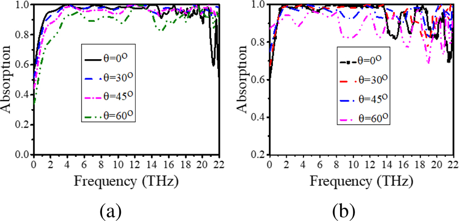
Polarization insensitivity is useful for absorbers in practical applications. Therefore, the absorption under different polarized wave and incident angles is investigated. The absorption spectra of the proposed UWB-MMA are almost constant due to the symmetry of the rotation of the proposed configuration. As shown in Fig. 9. even when the polarization angle is between 0 and 45 for both TM and TE modes, the absorption spectra are still above 90% in the whole bandwidth. The UWB absorption efficiency will gradually decrease beyond 45 particularly for the lower frequency range for TE waves, as shown in Fig. 9 (b). That is why the magnetic flux between the ground plane and the graphene layer reduces as the angle of incidence TE waves increases [38]. Moreover, with the rise in the oblique incidence angle, the frequency spectrum of greater absorption has a small blue change.
The strong absorption of the UWB band frequency for TM waves can be sustained up to 60, as seen in Fig. 9 (a). This means that at a higher incidence angle, the magnetic flux between the graphene layer and the ground layer is practically unchanged for the TM waves [38]. However, the absorption spectra for the proposed UWB-MMA also reveal a slight blue change with increasing angles of incidence for the TM wave. These findings demonstrate that both TE and TM waves can sustain absorption stability with varying polarization angles as well as large incident angles.
(a)(b)
Figure 9: The absorption spectra of the proposed UWB-MMA under normal different incident angles (a) TM waves, and (b) TE waves.
IV. CONCLUSION
In this paper, we have proposed UWB tunable MMA based on the “E” shape graphene pattern on a gold layer separated by a dielectric substrate. Numerically calculated results demonstrate that the suggested MMA attains higher absorption of over 95% in the frequency range of 1.12-14.04 THz, and the associated relative bandwidth is up to 170% to the central frequency. This UWB absorption is produced through localized surface plasmon and graphene surface plasmon stacking at various frequencies. To better understand the processes of absorption, we examined the electric field amplitude distribution at various frequencies. Thus, as the proposed structure is symmetrical, there is no significant difference between the TM and TE polarized waves it is not sensitive to wide angle of incidence wave. Furthermore, we have also discussed the influence of the permittivity and thickness of the substrate and Fermi energy level of the graphene over the absorption spectrum of the MMA.
REFERENCES
[1] J. Federici and L. Moeller, “Review of terahertz and sub terahertz wireless communications,” Journal of Applied Physics, vol. 107, no. 11, pp. 111101-111101-22, 2010.
[2] P. U. Jepsen, D. G. Cooke, M. Koch, and P. Reviews, “Terahertz spectroscopy and imaging–modern techniques and applications,” Laser & Photonics Reviews, vol. 5, no. 1, pp. 124-166, 2011.
[3] M. Liu, X. Yin, E. Ulin-Avila, B. Geng, T. Zentgraf, L. Ju, F. Wang, and X. Zhang, “A graphene-based broadband optical modulator,” Nature, vol. 474, no. 7349, pp. 64-67, 2011.
[4] H. Tao, N. I. Landy, C. M. Bingham, X. Zhang, R. D. Averitt, and W. Padilla, “A metamaterial absorber for the terahertz regime: design, fabrication and characterization,” Optics Express, vol. 16, no. 10, pp. 7181-7188, 2008.
[5] X. Zhang, Y. Qi, P. Zhou, H. Gong, B. Hu, and C. J. P. S. Yan, “Refractive index sensor based on fano resonances in plasmonic waveguide with dual side-coupled ring resonators,” Photonic Sensors, vol. 8, no. 4, pp. 367-374, 2018.
[6] H. Lin, X. Ye, X. Chen, Z. Zhou, Z. Yi, G. Niu, Y. Yi, Y. Hua, J. Hua, and S. Xiao, “Plasmonic absorption enhancement in graphene circular and elliptical disk arrays,” Materials Research Express, vol. 6, no. 4, pp. 0-8, 2019.
[7] Z. Fang, S. Thongrattanasiri, A. Schlather, Z. Liu, L. Ma, Y. Wang, P. M. Ajayan, P. Nordlander, N. J. Halas, and F. J. García De Abajo, “Gated tunability and hybridization of localized plasmons in nanostructured graphene,” ACS Nano, vol. 7, no. 3, pp. 2388-2395, 2013.
[8] S. Thongrattanasiri, F. H. Koppens, and F. J. García de Abajo, “Complete optical absorption in periodically patterned graphene,” Physical Review Letters, vol. 108, no. 4, pp. 1-5, 2012.
[9] V. Kumar, “24 GHz graphene patch antenna array,” Applied Computational Electromagnetics Society (ACES) Journal, vol. 34, no. 5, pp. 676-683, 2019.
[10] S.-L. Wang, J.-S. Hong, Y. Deng, and Z.-J. Chen, “A frequency reconfigurable antenna based on few layers graphene,” Applied Computational Electromagnetics Society (ACES) Journal, vol. 36, no. 5, pp. 542-547, 2021.
[11] R. Bala, R. Singh, A. Marwaha, and S. Marwaha, “Wearable graphene based curved patch antenna for medical telemetry applications,” Applied Computational Electromagnetics Society (ACES) Journal, vol. 31, no. 5, pp. 543-550,2016.
[12] J. Huang, Y. Wu, B. Su, and J. Liu, “Preparation and electrical testing of double top gate graphene field-effect transistor,” Applied Computational Electromagnetics Society (ACES) Journal, vol. 37, no. 7, pp. 774-781, 2022.
[13] M. Sajjad, X. Kong, S. Liu, S. U. Rahman, and J. Han, “Design of ultra-wideband tunable cross polarization converter based on a graphene,” International Applied Computational Electromagnetics Society (ACES) Symposium, Nanjing, China, pp. 1-2, August 2019.
[14] L. Guo, S. Li, X. Jiang, X. Liao, and L. Peng, “Ultra-wideband transmissive linear polarization device based on graphene,” Applied Computational Electromagnetics Society (ACES) Journal, vol. 36, no. 7, pp. 914-921, 2021.
[15] M. Huang, Y. Cheng, Z. Cheng, H. Chen, X. Mao, and R. Gong, “Based on graphene tunable dual-band terahertz metamaterial absorber with wide-angle,” Optics Communications, vol. 415, pp. 194-201, 2018.
[16] S. Biabanifard, M. Biabanifard, S. Asgari, S. Asadi, and C. Mustapha, “Tunable ultra-wideband terahertz absorber based on graphene disks and ribbons,” Optics Communications, vol. 427, pp. 418-425, 2018.
[17] Y. Dong, P. Liu, D. Yu, G. Li, L. J. I. A. Yang, and W. P. Letters, “A tunable ultrabroadband ultrathin terahertz absorber using graphene stacks,” IEEE Antennas and Wireless Propagation Letters, vol. 16, pp. 1115-1118, 2016.
[18] B. Xiao, M. Gu, and S. Xiao, “Broadband, wide-angle and tunable terahertz absorber based on cross-shaped graphene arrays,” Applied Optics, vol. 56, pp. 5458-5462, 2017.
[19] H. P. Xin, F. Liu, G. J. Ren, H. L. Zhao, and J. Q. Yao, “A liquid crystals modulated optical tunable filter based on Fano resonance of Au nanorod trimer,” Optics Express, vol. 389, pp. 92-96, 2017.
[20] P. D. Cunningham, N. N. Valdes, F. A. Vallejo, L. M. Hayden, B. Polishak, X. H. Zhou, J. Luo, A. K. Y. Jen, J. C. Williams, and R. J. Twieg, “Broadband terahertz characterization of the refractive index and absorption of some important polymeric and organic electro-optic materials,” Journal of Applied Physics, vol. 109, no. 4, pp. 043505-043505-5, 2011.
[21] N. Liu, L. Langguth, T. Weiss, J. Kästel, M. Fleischhauer, T. Pfau, and H. Giessen, “Induced transparency at the Drude damping limit,” Nature Materials, vol. 8, pp. 758-763, 2009.
[22] C. R. Dean, A. F. Young, I. Meric, C. Lee, L. Wang, S. Sorgenfrei, K. Watanabe, T. Taniguchi, P. Kim, K. L. Shepard, and J. Hone, “Boron nitride substrates for high-quality graphene electronics,” Nature Nanotechnology, vol. 5, no. 10, pp. 722-726, 2010.
[23] A. Khavasi, “Design of ultra-broadband graphene absorber using circuit theory,” Journal of the Optical Society of America B, vol. 32, pp. 1941-1946, 2015.
[24] C. Hwang, D. A. Siegel, S. K. Mo, W. Regan, A. Ismach, Y. Zhang, A. Zettl, and A. Lanzara, “Fermi velocity engineering in graphene by substrate modification,” Scientific Reports, vol. 2, pp. 1-4, 2012.
[25] G. W. Hanson, “Dyadic Green’s functions and guided surface waves for a surface conductivity model of graphene,” Journal of Applied Physics, vol. 103, no. 6, pp. 064302-064302-8, 2008.
[26] W. Gao, J. Shu, C. Qiu, and Q. Xu, “Excitation of plasmonic waves in graphene by guided-mode resonances,” ACS Nano, vol. 6, no. 9, pp. 7806-7813, 2012.
[27] S. Ke, B. Wang, H. Huang, H. Long, K. Wang, and P. Lu, “Plasmonic absorption enhancement in periodic cross-shaped graphene arrays,” Optics Express, vol. 23, no. 7, pp. 8888-8900, 2015.
[28] L. Ju, B. Geng, J. Horng, C. Girit, M. Martin, Z. Hao, H. A. Bechtel, X. Liang, A. Zettl, Y. R. Shen, and F. Wang, “Graphene plasmonics for tunable terahertz metamaterials,” Nature Nanotechnology, vol. 6, no. 10, pp. 630-634, 2011.
[29] Y. J. Kim, Y. J. Yoo, K. W. Kim, J. Y. Rhee, Y. H. Kim, and Y. Lee, “Dual broadband metamaterial absorber,” Optics Express, vol. 23, no. 4, pp. 3861-3868, 2015.
[30] M. L. Huang, Y. Z. Cheng, Z. Z. Cheng, H. R. Chen, X. S. Mao, and R. Z. Gong, “Design of a broadband tunable terahertz metamaterial absorber based on complementary structural graphene,” Materials, vol. 11, no. 4, pp. 1-10, 2018.
[31] L. Ren, Q. Zhang, J. Yao, Z. Sun, R. Kaneko, Z. Yan, S. Nanot, Z. Jin, I. Kawayama, M. Tonouchi, J. M. Tour, and J. Kono, “Terahertz and infrared spectroscopy of gated large-area graphene,” Nano Letters, vol. 12, no. 7, pp. 3711-3715, 2012.
[32] A. Vakil and N. Engheta, “Transformation optics using graphene,” Science, vol. 332, no. 6035, pp. 1291-1294, 2011.
[33] D. Smith, S. Schultz, P. Markoš, and C. Soukoulis, “Determination of effective permittivity and permeability of metamaterials from reflection and transmission coefficients,” Physical Review, vol. 65, no. 19, pp. 1-5, 2002.
[34] J. Huang, J. Li, Y. Yang, J. Li, Y. Zhang, and J. Yao, “Active controllable dual broadband terahertz absorber based on hybrid metamaterials with vanadium dioxide,” Optics Express, vol. 28, no. 5, pp. 7018-7027, 2020.
[35] H. Shen, F. Liu, C. Liu, D. Zeng, B. Guo, Z. Wei, F. Wang, C. Tan, X. Huang, and H. Meng, “A polarization-insensitive and wide-angle terahertz absorber with ring-porous patterned graphene metasurface,” Nanomaterials, vol. 10, no. 7, pp. 1-11, 2020,
[36] O. M. Daraei, K. Goudarzi, and M. J. O. Bemani, “A tunable ultra-broadband terahertz absorber based on two layers of graphene ribbons,” Optics & Laser Technology, vol. 122, pp. 105853-105835-9, 2020.
[37] T. Aghaee and A. A. Orouji, “Circuit modeling of ultra-broadband terahertz absorber based on graphene array periodic disks,” International Journal of Numerical Modelling: Electronic Networks, vol. 33, no. 3, pp. 1-13, 2020.
[38] Y. Cheng, H. Zou, J. Yang, X. Mao, and R. Gong, “Dual and broadband terahertz metamaterial absorber based on a compact resonator structure,” Optical Materials Express, vol. 8, no. 10, pp. 3104-3114, 2018.
BIOGRAPHIES

Muhammad Sajjad was born in 1990. He received the B.Sc. degree in Telecommunication from the University of Science and Technology, Bannu, Pakistan, in 2013, and the MSc. degree in Electrical Engineering from COMSAT University, Pakistan, in 2017. He is currently pursuing the Ph.D. degree with the Nanjing University of Aeronautics and Astronautics (NUAA), Nanjing, China. His research interests include electromagnetics and antennas especially metasurfaces, FSS, and polarization conversation.

Xiangkun Kong (Member, IEEE) received a Ph.D. degree in Communication and Information Systems from the Nanjing University of Aeronautics and Astronautics (NUAA), Nanjing, China, in 2015. He has been an Associate Professor with NUAA since his promotion in July 2015. He used to work at the University of St. Andrews, U.K., as an Academic Visitor supported by the China Scholarship Council. His main research interests include the electromagnetic properties of frequency selective surface, metamaterial and metasurface application, plasma photonic crystal, and computational electromagnetics. He has published more than 100 articles in different academic journals, including Applied Physics Letters, Optics Express, and IEEE Transactions on Antennas and Propagation, and has been cited 1600 times.
Shaobin Liu (Member, IEEE) received a Ph.D. in Electronics Science and Technology from the National University of Defense Technology, Changsha, China, in 2004. He is currently a Professor of Electromagnetic and Microwave Technology with the Nanjing University of Aeronautics and Astronautics, Nanjing, China. His current research interests include plasma stealthy antennas, microwave, radio frequency, and electromagnet incompatibility.

Saeed Ur Rahman is with school of Electronic Engineering, Xidian University, Xi’an, China. He has worked as a postdoctoral research fellow at Nanjing University of Aeronautics and Astronautics (NUAA), Nanjing China and also received his Ph.D. degree in information and communication engineering from NUAA. Currently he is an Associate Professor at Xidian University, Xi’an China.
Zakir Khan received his B.Sc. Engineering degree in Telecommunication Engineering from the University of Engineering and Technology, Peshawar, Pakistan, in 2013, the M.Sc. degrees in Electrical Engineering from COMSATS Institute of Information and Technology, Abbottabad, Pakistan in 2016 and the Ph.D. degree with Department of Electronics science and Technology, University of Science and Technology of China in 2022. His research interests include microwave and millimeter wave antenna design, microstrip patch antennas, miniaturized antennas, wide band antennas and multiband antennas.

Owais received the B.Eng. and M.Sc. degrees from the University of Engineering and Technology, Peshawar, Pakistan, in 1996 and 2000, respectively, and the Ph.D. degree in Communication Electronics from the Department of Science and Technology, Linköping University, Sweden. He is currently serving as an Associate Professor with the COMSATS University Islamabad, Abbottabad Campus, Pakistan. He has authored 40 international journal articles. His main research interests include the design of microstrip patch and dielectric resonator antennas, MIMO and reconfigurable DRAs, electromagnetic bandgap, and double-negative metamaterials; moreover, six-port front-end circuits for direct conversion transceiver design and high-speed data transmissions are also his area of interest.
ACES JOURNAL, Vol. 38, No. 2, 129–136
doi: 10.13052/2023.ACES.J.380207
© 2023 River Publishers