Design and Evaluation of Ultra-broadband Metamaterial Absorber for Energy Harvesting Applications
Ebenezer Abishek, Elakkiya Azhagar, Manikandan Esakkimuthu, and Karthigeyan Arumugam
1Associate Professor, Department of Electronics and Communication Engineering
Vel Tech Multi Tech Dr. Rangarajan Dr. Sakunthala Engineering College, Chennai-600062, India
ebenezerabishek@gmail.com
2Department of Electronics and Communication Engineering
Saveetha Engineering College, Chennai- 602105, India
3Center for Innovation and Product Development, School of Electronics Engineering
Vellore Institute of Technology, Chennai- 600127, India
4Department of Electronics and Communication Engineering
Vel Tech Rangarajan Dr. Sagunthala R&D Institute of Science
and Technology, Chennai- 600062, India
Submitted On: November 19, 2022; Accepted On: June 8, 2023
ABSTRACT
A perfect metamaterial absorber (MMA) is designed and evaluated numerically for solar energy harvesting applications. A dielectric layer separates the top structured metallic plane and the bottom ground metallic plane that make up the MMA. The MMA structure is primarily presented in the range of 100-1000 THz, which corresponds to 3000-300 nm in wavelength, for the efficient utilization of solar energy. The results obtained in the band 441-998 THz correspond to a visible and ultraviolet wavelength range of 680-300 nm. It has achieved a maximum absorption rate of 99.9% at 700 THz and 99% between 500 and 800 THz, respectively. In the desired frequency bands, the structure has achieved polarization and angle-resolved behavior. The MMA-based absorber has a high absorption rate of over 90% in the broadest visible (400-700 nm) and UV (100-300 nm) spectra. Also shown are the absorption characteristics of the MMA-based solar cell in the infrared (IR) region. The band 345-440 THz, corresponding to 870-690 nm, has 75% absorption. The other IR band (240-345 THz), which corresponds to 1250-880 nm, has achieved absorption of nearly 50%. So it can be utilized for the entire visible solar spectrum, including infrared to ultraviolet. If the proposed MMA structure were equipped with the appropriate electrical circuitry, it could be utilized for solar energyharvesting.
Index Terms: absorber, energy harvesting, metamaterial, solar.
I. INTRODUCTION
The distinction between renewable and nonrenewable energy sources is made. Included in fossil fuels are coal, oil, and petroleum. Excessive use depletes resources. Natural gas will last 60 years, petroleum 40 years, and coal 200 years [1]. The combustion of these fuels in automobiles and power plants produces greenhouse gases that contribute to global warming. Renewable energies such as geothermal, tidal, hydroelectric, solar, and wind are all free. These resources are plentiful, non-perishable, and environment friendly. Energy demand has increased due to technological advancements, rising populations, and industrial expansion. Available fossil fuels cannot meet energy demands [2]. Solar energy is a renewable substitute for fossil fuels Solar can be divided into three major regions: infrared (52%), visible (39%), and ultraviolet (9%), approximately. In one hour, solar emissions can meet the world’s annual energy needs [3–4]. However, this source is difficult to harvest. Solar cells convert incident solar energy into electricity, but their low conversion efficiency presents a challenge for scientists. The material’s bandgap corresponds to the absorption of incident photon energy. Solar cells convert absorbed electrons into electric current. The corresponding frequency band is in the range of 100-1000THz [7]. To improve absorption, scientists are researching nanomaterials and nanostructure-based absorbers, solar cell concentrators, embedded solar cell systems, etc. Solar trackers enhance absorption in accordance with environmental conditions. A device with improved absorption characteristics is required to absorb incident energy regardless of polarization or angle. These issues must be addressed by solar cells. Non-natural metamaterials possess extraordinary properties, such as negative refraction and cloaking [8–9]. Metamaterials are used to construct electromagnetic (EM) energy absorbers that are more efficient. Metamaterials are synthetic materials with peculiar properties and benefits, such as evanescent wave amplification, invisibility cloaking, superlenses, electromagnetic filters, sensors, antennas, high-frequency polarization rotators, a negative refractive index, and negative permeability [10–15]. This is not normal. Recently, there has been increased interest in metamaterials as absorbers [16–20]. A metamaterial absorber (MMA) can collect sunlight to increase the efficiency of solar cells. In the THz and microwave regions, MMA was developed for shielding, sensing, etc. Perfect index sensing based on MMA is also described [21]. The resonance of MMA is governed by geometric parameters and material properties [22]. Exotic, high-frequency MMA is created between the visible and ultraviolet regimes [23–30]. Similar outcomes are observed in the infrared [31–34]. These are narrowband designs. Many MMA competitors used low-frequency techniques. Therefore, the design of solar MMA must have broad absorption. Solar energy harvesting will require a broadband metamaterial absorber. In this paper, a new MMA structure with broadband absorption characteristics is designed. Variations in the geometric parameters of the structure produce different absorption characteristics. It absorbs infrared, visible, and ultraviolet radiation. The engineered structure possesses pseudo-plasmon frequencies. By optimizing the model’s geometric parameters and dielectric substrate, its resonance is modified. 90% of visible light is absorbed, with a peak absorption of 99% in the 500-800THz band. As a reflector, the bottom metal plate increases absorption.
II. MATERIALS AND STRUCTURE
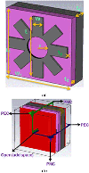
The perspective view of the proposed MMA and the boundary conditions are shown in Figs. 1 (a) and (b), respectively. The numerical simulation of the designed structure is carried out using CST Microwave Studio software in a high-frequency finite element analysis approach. The structure has three layers: a structured top metallic patch, a bottom metallic ground plane, and an intermediate dielectric substrate. The metal is tungsten (W), and the substrate is silicon dioxide (SiO). The properties of these materials at the desired frequencies are used as given by Ghosh (1999) and Palik (1997). The advantages of using tungsten are that it has a higher melting point and better solar absorption characteristics than the other metals. Furthermore, SiO allows for greater flexibility in solar cell integration, which improves absorption even further. This eases the fabrication process as well.
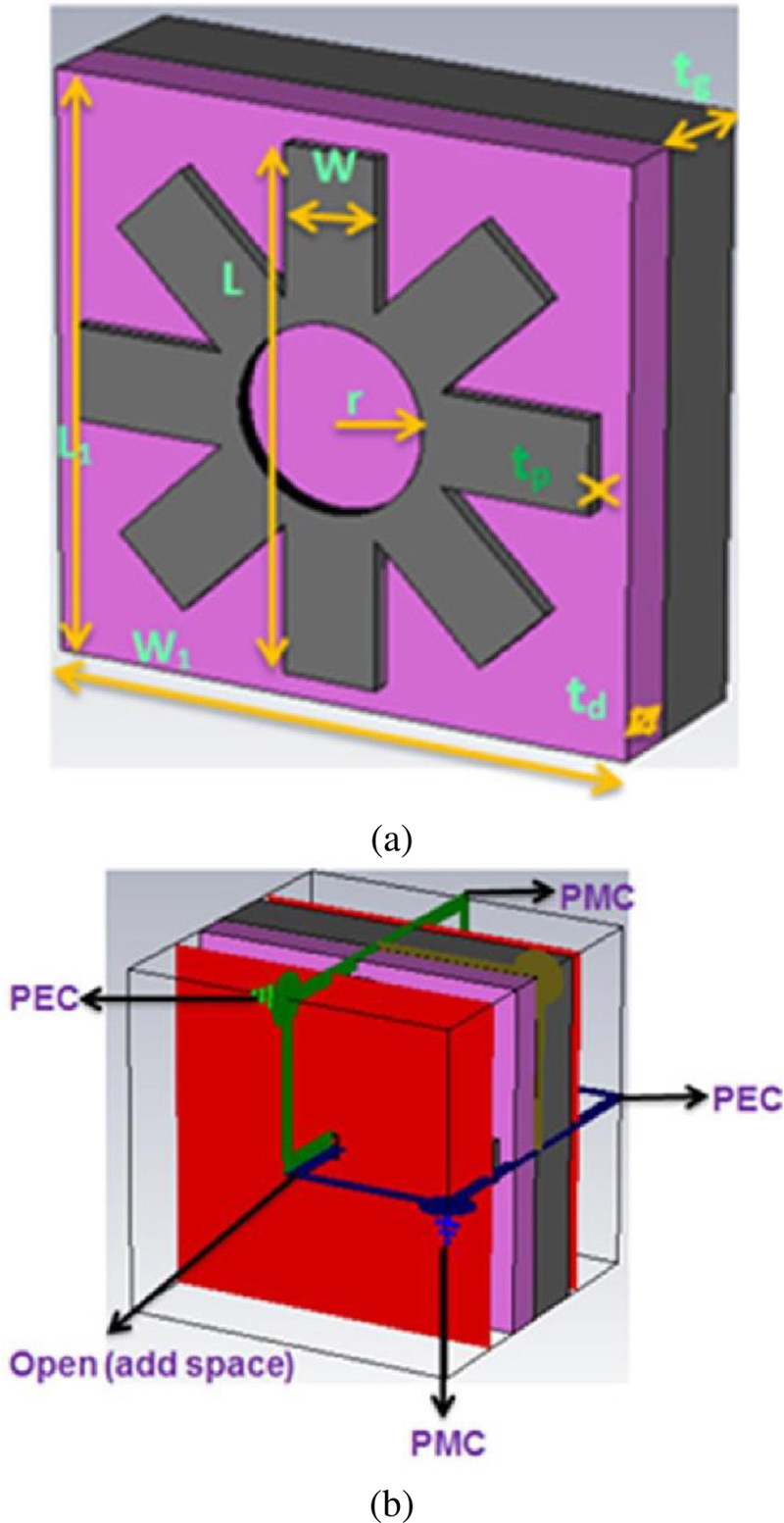
Figure 1: (a) Geometry of the unit cell of the proposed MMA, perspective view. [Geometrical parameters: L= W = 500 nm, W = 80 nm, L = 450 nm, r = 80 nm, t = 15 nm, t = 60 nm, t = 100 nm], (b) Boundary conditions.
III. ABSORPTION AND SIMULATION STUDIES
In simulation, unit cell periodic boundary conditions in the x and y directions and open space in the z-direction are utilized. The wave is incident on the top metallic patch using the floquet port, and the output is measured at the backside of the bottom ground plane. This kind of setup avoids any near-field problems. By using parametric analysis, the best dimensions for the proposed MMA can be found and are shown in Fig. 1 (a). The electromagnetic spectrum is divided into different regions, but the majority of solar energy that reaches the earth belongs to the visible, infrared, and ultraviolet (UV) regions. So this region, i.e., 100-1000 THz, is chosen for the analysis, and the MMA is designed. The incident solar EM radiation may be either absorbed, reflected, or transmitted. The absorption value is calculated indirectly by obtaining the reflection and transmission values. For better absorption, reflection and transmission should be kept to a minimum. The thickness of the bottom ground plane is kept higher to avoid any transmission through it, i.e., a thinner layer transmits more. The transmitted wave power is considered to be zero due to the presence of a metallic ground plane that reflects the incident EM radiation. So the objective is to minimize the reflection. The following will be used for the calculation of the absorption:
| (1) |
From equation (1) it is evident that for obtaining maximum absorption, the reflection in the structure should be kept minimum. This can be achieved by proper impedance matching where the free space impedance matches with the structure impedance (Z = Z). Therefore, the transmission and reflection should be negligible for obtaining better absorptioncharacteristics.
IV. RESULTS AND DISCUSSION
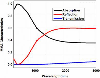
The obtained absorption, reflection, and transmission characteristics of the proposed structure for the desired geometrical parameters are shown in Fig. 2. The proposed MMA has obtained near-perfect absorption of about 99.9% at the frequency of 700 THz, with broadband absorption behavior of about 90% in the entire solar spectrum. The amount of light that is absorbed is more than 90% across the entire range of visible and ultraviolet (UV) light. The bottom metallic layer acts as a good reflector, and in addition, the lossy nature of the dielectric supports perfect absorption. The dielectric substrate and unit cell dimensions will determine the resonance. The structured top metallic patch determines the resonant characteristic of the MMA. As a result, all of these must be carefully chosen in order to achieve perfect absorption in the desired band.
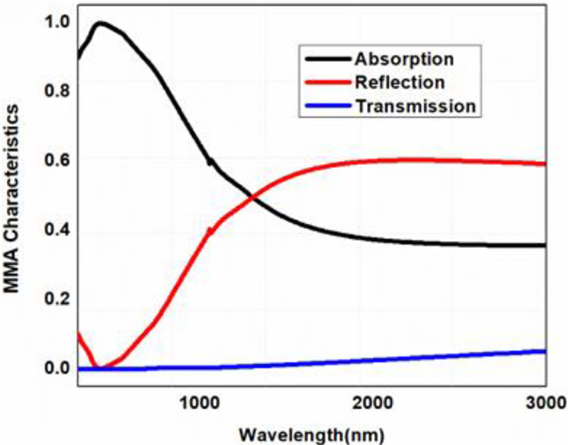
Figure 2: Wavelength versus characteristics of the designed MMA.
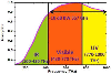
From the wavelength vs. absorption spectrum, the respective frequency is extracted. The absorption characteristics of the proposed MMA are also observed for wider frequency ranges, including infrared (IR), visible light, and UV regions, which are shown in Fig. 3.
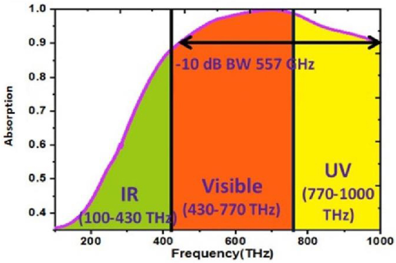
Figure 3: The absorption rate of the proposed structure in the solar light regime (100-1000 THz).
It is obvious that absorption of more than 70% is seen even in the infrared region between 300 and 430 THz, which is an indicator that the proposed structure can also be utilized for IR photodetector applications.
Likewise, it is clear that the absorption value of the proposed MMA in the UV region is also above 90% in the frequency range between 770 and 1000 THz. Based on these features, it can be said that the proposed MMA can be used not only for solar energy harvesting but also as a photodetector.
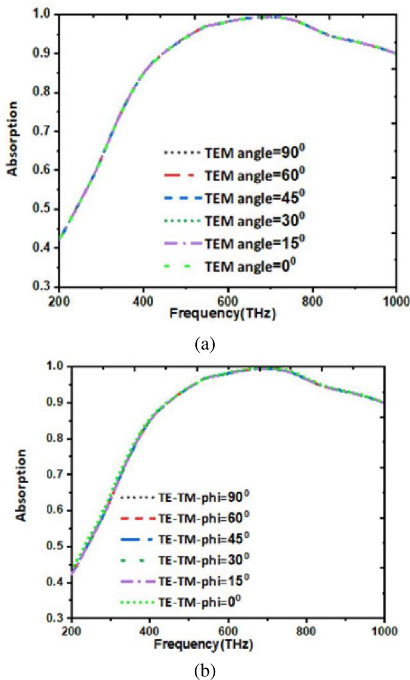
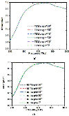
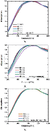
Figure 4: (a) The absorption spectra TEM mode various incident angles for TE mode. (b) The absorption spectra TEM mode for various incident angles for TM mode.
Figures 4 (a) and 4 (b) show the absorption characteristics of the designed structure for different modes at various angles of incidence. This is evidence for the proposed structure’s absorption characteristics, independent of the incidence angles varying from 0 to 90. Therefore, the proposed structure could be utilized for absorbing the incident solar energy even at different incidence angles for all polarizations. Since most research only looks at transverse electric (TE) and transverse magnetic (TM) polarization, this adds importance to the proposed structure for analysis.
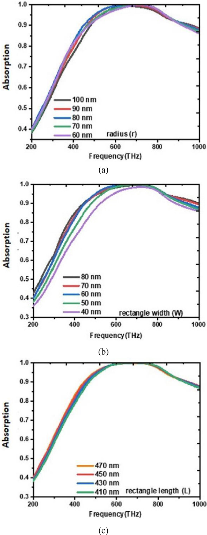
Figure 5: (a) absorption rate changes with respect to radius, (b) absorption rate changes with respect to rectangle width, and (c) absorption rate changes with respect to rectangle length.
V. PARAMETRIC ANALYSIS
The geometrical parameters of the proposed structure are depicted in Fig. 1. The parametric study can be used to find out how the size of a part affects the frequency at which it works. The study is done for three geometric parameters, each of which is changed one at a time, and their absorption properties are found.
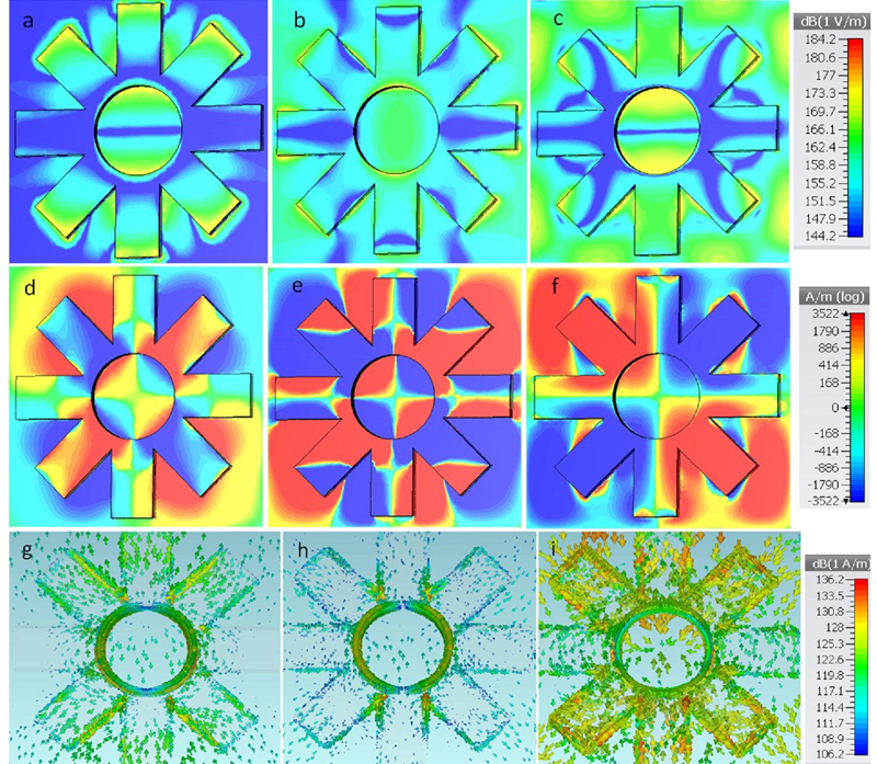
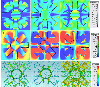
Figure 6: (a-c) Electric field; (d-f) magnetic field; (g-i) surface current distributions for the three resonances 441 THz, 700 THz, and 998 THz, respectively.
The effects of changing the inner radius (r), rectangle width (W), and rectangle length (L) of the patch on the absorption spectra are as follows. By changing r from 60 to 100 nm (keeping W at 80 nm, L at 450 nm), W from 40 to 80 nm (keeping L at 450 nm, r at 80 nm), and L from 410 to 470 nm (keeping W at 80 nm, r at 80 nm), the resonance modes drift to lower frequencies, as shown in Figs. 5 (a), (b), and (c), respectively. From this analysis, the parameters r = 80 nm, W = 80 nm, and L = 450 nm are chosen as the desired parameters for the designed structure for better absorption.
VI. FIELD DISTRIBUTIONS AND ANALYSIS
For understanding the primary physical mechanism of the proposed MMA, the distributions of the electric field at the three resonant frequencies are shown in Figs. 6 (a-c). A similar star-shaped resonator without any aperture was presented [22]. But it was focused only on the visible region and obtained a bandwidth of around 300 THz. In considering three bands (IR, visible, and UV), three peak resonant frequencies (441 THz, 700 THz, and 998 THz) are chosen for analysis. The electric field distribution confirms that only vertical and diagonal elements are contributing at 441 THz, but all elements are participating at 700 THz. It is noted that in addition to the resonating elements, the circular aperture and the substrate also contribute to the third resonance, i.e., 998 THz. This is how the proposed design is differentiated to absorb different regions of the solar spectrum [22]. The corresponding y-component of the magnetic field distributions is also depicted in Figs. 6 (d-f). For the resonances at 441 THz and 700 THz, the magnetic field is high throughout the whole patch structure and in the dielectric substrate layer as well. Also observed is the excitation of quad polar, octa polar, and other higher resonances in the magnetic field distributionanalysis.
The current distributions through the surface of the metamaterial are also observed and shown in Figs. 6 (g-i). At 441 THz, vertical and diagonal resonating elements are responsible. Similarly, at 700 THz and 998 THz, the circular aperture and the entire resonator are contributing to the respective resonances.
In order to validate the importance of this work, the results are compared with the recent literatures related to this work and shown in Table 1.
Table 1: Comparison between the earlier studies in the literature and proposed absorber
| Ref. | Band (THz) | Obtained Bandwidth (GHz)(Absorption ) |
|---|---|---|
| [17] | 69-72 | 5 |
| [19] | 75-85 | 10 |
| [31] | 40-70 | 30 |
| [29] | 60-115 | 55 |
| [30] | 175-300 | 125 |
| [22] | 430-770 | 340 |
| [6] | 450-700 | 250 |
| [34] | 500-800 | 300 |
| [7] | 300-500 | 200 |
| This work | 441-998 | 557 |
The absorption value and the bandwidth determine the performance of the structure. The absorption rate of a minimum of 90% is considered for the analysis. A comparison with the literature is presented in Table 1 given above. The important point to note is that the proposed structure achieved broadband operation with better absorption characteristics than the previously reported works. It is evident that the structure is simple and obtained a broadband absorption of 557 GHz bandwidth, which is 2-3 times better than the earlier reportedworks.
The structure’s thickness is 175 nm, indicating that it is thinner and more flexible. This absorption capability and size makes it efficient for capturing solar radiation. Independently, it can work as an energy harvesting module with proper electrical circuits, or it can be integrated with the solar cell as an absorbing medium.
Fabrication Feasibility and Real-time Characterization:
The proposed structure has two materials: a dielectric substrate and the conducting patch/ground plane. The conducting material, copper, can be deposited using the sputtering technique, which can yield the nm thickness easily. The major advantage of this proposed structure is that the dimensions are in the order of 100 nm with a minimum feature of 80 nm. Using a lithography process like E-beam or etching techniques like reactive ion etching, the minimum feature with high resolution could be achieved. Overall, the proposed structure is simple to fabricate with the mentioned facilities. The real-time measurements can be done with UV-visible spectroscopy for the absorption characteristics.
VII. CONCLUSION
A three-layered ultra-broadband MMA is designed and evaluated numerically. The structure absorbs 99.9% of 700 THz and 99% of 500-800 THz. It absorbs over 90% of visible (400-700) nm and UV (100-200) nm light. The MMA-based solar cell for the infrared absorption is also studied, i.e., 345-440 THz, or 870-680 nm in wavelength which is having around 75% absorption. The other IR band (1250-870 nm/240-345 THz) absorbs nearly 50% of the incident radiation. The structure has polarisation and angle-resolved behaviour in the desired bands. Resonance electric and magnetic field distribution analysis investigates broadband absorption. By integrating proper electrical circuits to the MMA, incident energy can be directly converted into electrical energy. This W-SiO absorber could be used for detector application also.
REFERENCES
[1] B. Li, L. Wang, B. Kang, P. Wang, and Y. Qiu, “Review of recent progress in solid-state dye-sensitized solar cells,” Solar Energy Materials and Solar Cells, vol. 90, no. 5, pp. 549-573, 2006.
[2] M. P. Ustunsoy and C. Sabah, “Dual-band high-frequency metamaterial absorber based on patch resonator for solar cell applications and its enhancement with graphene layers,” Journal of Alloys and Compounds, vol. 687, pp. 514-520, 2016.
[3] A. V. Getman, M. G. Dushejko, A. V. Ivashchuk, M. S. Fadieiev, and Y. I. Yakymenko, “Influence of the carrier lifetime on the silicon solar cells radiation resistance,” IEEE 34th International Scientific Conference on Electronics and Nanotechnology (ELNANO), pp. 227-229, 2014.
[4] Z. L.Wang and W. Wu, “Nanotechnology-enabled energy harvesting for self-powered micro-/nanosystems,” Angew. Chem. Int. Ed., vol. 51, pp. 11700-11721, 2012.
[5] F. Dincer, O. Akgol, M. Karaaslan, E. Unal, and C. Sabah, “Polarization angle independent perfect metamaterial absorbers for solar cell applications in the microwave, infrared, and visible regime,” Progress in Electromagnetics Research, vol. 144, pp. 93-101, 2014.
[6] P. Rufangura and C. Sabah, “Dual-band perfect metamaterial absorber for solar cell applications,” Vacuum, vol. 120, part B, pp. 68-74, 2015.
[7] B. Mulla and C. Sabah, “Perfect metamaterial absorber design for solar cell applications,” Waves in Random and Complex Media, vol. 25, no. 3, pp. 382-392, 2015.
[8] Y. Avitzour, Y. A. Urzhumov, and G. Shvets, “Wide-angle infrared absorber based on a negative-index plasmonic metamaterial,” Phys. Rev. B, vol. 79, pp. 045131-045136, 2009.
[9] J. Wang, C. Fan, P. Ding, J. He, Y. Cheng, W. Hu, G. Cai, E. Liang, and Q. Xue, “Tunable broad-band perfect absorber by exciting of multiple plasmon resonances at optical frequency,” Opt Express, vol. 20, no. 14, pp. 14871-14878, 2012.
[10] B. Wang, T. Koschny, and C. M. Soukoulis, “Wide-angle and polarization-independent chiral metamaterial absorber,” Phys. Rev. B, vol. 80, pp. 033108-033111, 2009.
[11] B.-X. Wang, X. Zhai, G.-Z. Wang, W.-Q. Huang, and L.-L. Wang, “Frequency tunable metamaterial absorber at deep-subwavelength scale,” Opt. Mater. Express, vol. 5, pp. 227-235, 2015.
[12] R. A. Shelby, D. R. Smith, and S. Schultz, “Experimental verification of a negative index of refraction,” Science, vol. 292, no. 5514, pp. 77-79, 2001.
[13] D. R. Smith, W. J. Padilla, D. C. Vier, S. C. Nemat-Nasser, and S. Schultz, “Composite medium with simultaneously negative permeability and permittivity,” Phys. Rev. Lett, vol. 84, no. 18, pp. 4184-4187, 2000.
[14] N. I. Landy, S. Sajuyigbe, J. J. Mock, D. R. Smith, and W. J. Padilla, “Perfect metamaterial absorber,” Phys. Rev. Lett., vol. 100, pp. 207402-207405, 2008.
[15] L. Huang and H. Chen, “Multi-band and polarization insensitive metamaterial absorber,” Progress in Electromagnetics Research, vol. 113, pp. 103-110, 2011.
[16] J. Yang, S. Qu, H. Ma, J. Wang, and Y. Pang, “Dual-band tunable infrared metamaterial absorber with VO conformal resonators,” Optics Communications, vol. 402, pp. 518-522, 2017.
[17] L. Li, Y. Yang, and C. Liang, “A wide-angle polarization-insensitive ultra-thin metamaterial absorber with three resonant modes,” Journal of Applied Physics, vol. 110, no. 6, pp. 063702,2011.
[18] W. Ma, Y. Wen, and X. Yu, “Broadband metamaterial absorber at mid-infrared using multiplexed cross resonators,” Opt Express, vol. 21, no. 25, pp. 30724-30730, 2013.
[19] N. Liu, M. Mesch, T. Weiss, M. Hentschel, and H. Giessen, “Infrared perfect absorber and its application as plasmonic sensor,” Nano Letters, vol. 10, no. 7, pp. 2342-2348, 2010.
[20] M. Bagmanci, M. Karaaslan, E. Unal, O. Akgol, M. Bakr, and C. Sabah, “Solar energy harvesting with ultra-broadband metamaterial absorber,” International Journal of Modern Physics B, vol. 33, no. 08, pp. 1950056, 2019.
[21] W. Zhou, K. Li, C. Song, P. Hao, M. Chi, M. Yu, and Y. Wu, “Polarization-independent and omnidirectional nearly perfect absorber with ultra-thin 2D subwavelength metal grating in the visible region,” Opt. Express, vol. 23, pp. A413-A418,2015.
[22] M. Bağmanci, M. Karaaslan, E. Ünal, O. Akgöl, and C. Sabah, “Extremely-broad band metamaterial absorber for solar energy harvesting based on star shaped resonator,” Optical and Quantum Electronics, vol. 49, no. 7, 2017.
[23] F. Dincer, M. Karaaslan, E. Unal, K. Delihacioglu, and C. Sabah, “Design of polarization and incident angle insensitive dual-band metamaterial absorber based on isotropic resonators,” Progress in Electromagnetics Research, vol. 144, pp. 123-132,2014.
[24] B. Mulla and C. Sabah, “Perfect metamaterial absorber design for solar cell applications,” Waves in Random and Complex Media, vol. 25, no. 3, pp. 382-392, 2015.
[25] P. Pitchappa, C. P. Ho, P. Kropelnicki, N. Singh, D.-L. Kwong, and C. Lee, “Micro-electro-mechanically switchable near infrared complementary metamaterial absorber,” Appl. Phys. Lett., vol. 104, no. 20, pp. 201114, 2014.
[26] P. Rufangura and C. Sabah, “Polarization angle insensitive dual-band perfect metamaterial absorber for solar cell applications,” Phys. Status Solidi C, vol. 12, pp. 1241-1245, 2015.
[27] X. Duan, S. Chen, W. Liu, H. Cheng, Z. Li, and J. Tian, “Polarization-insensitive and wide-angle broadband nearly perfect absorber by tunable planar metamaterials in the visible regime,” Journal of Optics, vol. 16, no. 12, 2014.
[28] W. Zhou, K. Li, C. Song, P. Hao, M. Chi, M. Yu, and Y. Wu, “Polarization-independent and omnidirectional nearly perfect absorber with ultra-thin 2D subwavelength metal grating in the visible region,” Opt. Express, vol. 23, pp. A413-A418,2015.
[29] X. Ling, Z. Xiao, X. Zheng, J. Tang, and K. Xu, “Broadband and polarization-insensitive metamaterial absorber based on hybrid structures in the infrared region,” Journal of Modern Optics, vol. 64, no. 7, pp. 665-671, 2017.
[30] F. Ding, J. Dai, Y. Chen, J. Zhu, Y. Jin, and S. I. Bozhevolnyi, “Broadband near-infrared metamaterial absorbers utilizing highly lossy metals,” Sci Rep, vol. 6, 2016.
[31] X. Ling, Z. Xiao, and X. Zheng, “A three-dimensional broadband infrared metamaterial absorber based on the plasmonic and dipole resonance responses,” Plasmonics, vol. 13, pp. 175-180, 2018.
[32] R. Feng, W. Ding, L. Liu, L. Chen, J. Qiu, and G. Chen, “Dual-band infrared perfect absorber based on asymmetric T-shaped plasmonic array,” Opt Express, vol. 22, no. 5, 2014.
[33] N. Zhang, P. Zhou, S. Zou, X. Weng, J. Xie, and L. Deng, “Improving the mid-infrared energy absorption efficiency by using a dual-band metamaterial absorber,” Progress in Natural Science: Materials International, vol. 24, no. 2, pp. 128-133,2014.
[34] P. Rufangura and C. Sabah, “Design and characterization of a dual-band perfect metamaterial absorber for solar cell applications,” Journal of Alloys and Compounds, vol. 671, pp. 43-50,2016.
BIOGRAPHIES

Ebenezer Abishek is an associate professor in the Department of Electronics and Communication Engineering, Vel Tech Multi Tech Dr. Rangarajan Dr. Sakunthala Engineering College. Has more than 10 years of teaching experience. In July of 2019, he earned a Ph.D. in electronics and communication engineering from the Vels Institute of Science, Technology, and Advanced Studies (VISTAS). Antennas, and electromagnetism are his research interests. He has published 33 articles in Scopus-indexed journals, two in SCI-indexed journals. The ORCID assigned to him is 0000-0003-2908-7069.

Elakkiya Azhagar is an assistant professor in the Department of Electronics and Communication Engineering, Saveetha Engineering College. She earned her doctorate degree from Sri Sivasubramaniam Nadar College of Engineering (SSN) in Chennai, India. Her current research is on terahertz devices like metamaterial absorbers, antennas, and filters.

Manikandan Esakkimuthu earned his Ph.D. in electrical engineering from Anna University in 2019. Currently, he is a senior assistant professor at the Vellore Institute of Technology, Chennai, in the Center for Innovation and Product Development (CIPD) and the School of Electronics Engineering. His areas of research interest are sensors and micromachining.

Karthigeyan Arumugam earned his Ph.D in information and communication engineering in 2022 from Anna University. Currently, he is an assistant professor in the Department of Electronics and Communication Engineering at Vel Tech Rangarajan Dr. Sagunthala R&D Institute of Science and Technology. His research interests currently include RF circuits and devices, terahertz applications, and hardware cybersecurity.
ACES JOURNAL, Vol. 38, No. 6, 416–423
doi: 10.13052/2023.ACES.J.380606
© 2023 River Publishers