Planar Antenna Design on the Characteristics of Moore Fractal-based High Impedance Surface
Akash K. Gupta, Paladuga S. R. Chowdary, and Mandhapati V. Krishna
1Research Scholar, Department of Electronics and Communication Engineering
Centurion University of Technology and Management, Odisha, 761211, India
akgupta452@gmail.com
2Department of Electronics and Communication Engineering
Raghu Engineering College, Visakhapatnam, Andhra Pradesh, 531162, India
satishchowdary@ieee.org
3Department of Electronics and Communication Engineering
Dhanekula Institute of Engineering and Technology, Vijayawada, Andhra Pradesh, 521139, India
vamshi51@yahoo.co.in
Submitted On: December 2, 2022; Accepted On: March 29, 2023
ABSTRACT
This work presents a planar antenna with a rectangular shape designed over a Moore curve fractal-shaped High Impedance Surface (HIS). The Moore fractal geometries are space-filling curves and are useful for multiband applications. The Moore curve-shaped fractal HIS is simulated up to three iterations, and performance is examined. The proposed antenna has multiband operation within the S-band, C-band, and lower X-band frequency of operation. The antenna has a peak gain of 5.08 dB, 4.69 dB, and 5.07 dB with a Moore curve fractal HIS, with iterations 1, 2, and 3 used as the ground plane. The antenna has been analyzed regarding the reflection coefficient, radiation pattern, 3-D polar plots, and surface current distribution. With Moore curve iteration 1, a shaped HIS provides a maximum bandwidth of 740 MHz with the center frequency of 10.95 GHz, 1.24 GHz with the center frequency of 10.57 GHz, and 1.09 GHz with the center frequency of 12.5 GHz with the second and third iterations, respectively.
Index Terms: High Impedance Surface (HIS), Moore curve fractals, rectangular patch antenna.
I. INTRODUCTION
Nowadays, microstrip patch antennas are preferred in many applications in field communications. The patch antennas have a wide range of applications and ease of use due to their low profile, light weight, ease of fabrication, and relatively low cost. The basic microstrip patch comprises a radiating patch followed by a dielectric media and ground plane. The radiation of the microstrip antenna depends on patch geometry as well as on the ground layer. In most cases, the ground plane consists of the Perfect Electric Conductor (PEC) due to its reflective properties that enhance antenna forward radiation and gain. The PEC ground plane has the limitation in that it causes a -phase shift between the reflected E-field and the incident field. The phase reversal fields result in ripples in an effective radiation pattern. Another disadvantage of this phase reversal reflected wave is that it forms an image current which leads to the formation of surface waves. Thus, normal and surface-wave radiation provides multipath propagation, leading to ripples in the radiation pattern. However, when the ground plane is spaced at 0.25 below the radiating patch, it will produce an in-phase current and constructive field. In practice, however, such thick substrates are not feasible for antenna applications. To address the problems of surface waves, High Impedance Surfaces are proposed [1]. These types of materials are frequently referred to as Pseudo Artificial Magnetic Conductors (AMCs) with a reflection phase responseof .
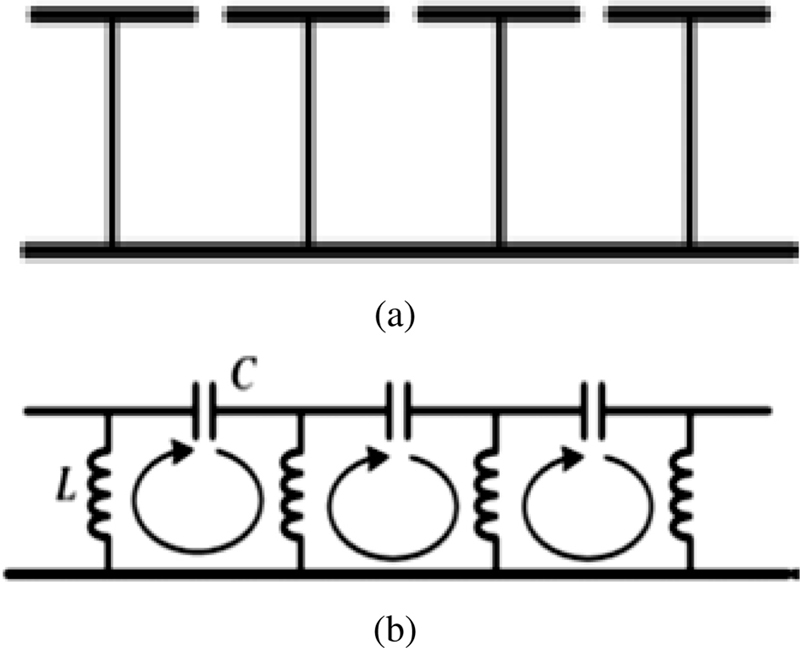
Figure 1: (a) HIS structure. (b) Equivalent circuit.
The high-impedance structure (HIS) is a two-dimensional periodic arrangement of metal patches [1]. These patches are spaced with uniform gaps and act as a sheet capacitance (C). Soldered vias are used to link these patches to the ground plane. The ground plane and the via will serve as an inductive sheet (L). Thus, a mushroom-shaped HIS [1] structure can be modeled using a parallel LC lumped circuit, as shown in Fig. 1. The resonance frequency of this equivalent circuit is given in equation (1) and impedance is given inequation (2):
| (1) |
| (2) |
where z = sheet impedance, C = sheet capacitance L = sheet inductance, and is the resonancefrequency.
The HIS characteristics are validated using the Finite Difference Time Domain (FDTD) model [2] and the Transmission line model [3]. The reflection phase characteristics of the mushroom shaped HIS are detailed in [4]. The mushroom-shaped HIS ground planes can be used for phased array radars [1]. The hexagonal-shaped HIS cells are used for tunable and steerable antennas [5], while the Generic Algorithm (GA)-optimized square-shaped fractal HIS structures are used for multiband AMC [6]. The non-uniform HIS structures are designed for bandwidth improvement [7]. The HIS-backed wire antenna [8] is proposed for scanning array applications. A via-less double-layer HIS for polarization-dependent structures, as described in [9], can generate linear and circular polarization. The HIS-based wideband antenna, proposed in [10], is for 14 GHz applications. The dog-bone-shaped HIS structure, proposed in [11], is for RFID and mobile applications, while the HIS-based Luneburg lens, proposed in [12], is for Ku band wave focusing applications. A wearable loop antenna fabricated over a textile surface based on HIS structure isinvestigated in [13].
This work proposes a Moore curve fractal-shaped HIS structure. The paper is organized as follows: Section I comprises the introduction and literature review, Section II deals with the antenna design methodology, including the design of a Moore curve-shaped HIS cell and rectangular microstrip antenna over the HIS array, and Section III describes the results andanalysis.
II. ANTENNA DESIGN METHODOLOGY
A. Moore curve-shaped HIS unit cell
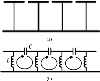
A Moore fractal curve is a fractal space-filling curve. It is a kind of Hilbert curve proposed by E. H. Moore. Fractal antennas can occupy a small area while covering a larger electrical path length [14]. Due to fractal and self-similar looping structures, they have many resonant frequencies. The Moore fractal curve from the first to the third iteration is illustrated in Fig. 2.
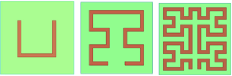
Figure 2: Moore fractal curve from the first to the third iteration.
A Moore curved HIS unit cell is carved over a square patch of . The Moore curve patches are designed on a flame retardant 4 substrate with a dielectric constant of 4.4, a loss tangent of 0.02, and a thickness of 1. 6 mm.
For the Moore curve HIS cells’ phase, reflection characteristics are examined. The effect of vias on reflection characteristics is tabulated in Table 1. For reflection characteristics, the useful bandwidth of a HIS surface has been defined as the range 90, and outside this range of frequencies, the reflected waves are mostly out of phase with the incident waves. As the antenna is intended to function in the X-band, the absence of vias doesn’t significantly affect reflection characteristics. Thus, the HIS is designed via-less for ease of fabrication.
B. Moore curve HIS-based rectangular microstrip antenna design
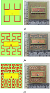
This work presents a rectangular patch antenna designed over a fractal-shaped Moore curve ground plane [14]. The Moore curve HIS rectangular microstrip antenna (MCHRMA) ground plane consists of a 2 2 array of Moore curve-shaped HIS unit cells. The geometry of the antenna is shown in Fig. 3: Fig. 3 (a) illustrates a rectangular radiator over a Moore curve first iteration HIS (MCHRMA-1), Fig. 3 (b) shows a rectangular radiator over a Moore curve in the second iteration HIS (MCHRMA-2), and Fig. 3 (c) shows a rectangular radiator over a Moore curve in the third iteration HIS (MCHRMA-3).
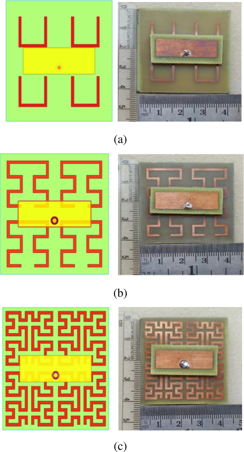
Figure 3: (a) Simulated and Fabricated MCHRMA_1. (b) Simulated and Fabricated MCHRMA_2. (c) Simulated and Fabricated MCHRMA_3.
The rectangular patch [15] is designed with dimensions of 28 9 over an FR4 substrate with dimensions of 30 11 and thickness of 1.6 mm from the MCH ground plane.
Table 1: Reflection phase characteristics of Moore curve HIS unit cell
| = = 20 mm with via ( | = = 20 mm without via | ||||||
|---|---|---|---|---|---|---|---|
| Design | Design | ||||||
| Moore Curve-shaped HISIteration 1 | – | – | – | Moore Curve-shaped HISIteration 1 | 2.91 | 2.90 | 2.92 |
| Moore Curve-shaped HISIteration 2 | 5.857.989.78 | 5.807.759.63 | 5.868.119.93 | Moore Curve-shaped HISIteration 2 | 5.897.929.68 | 5.827.79.55 | 5.918.089.83 |
| Moore Curve-shaped HISIteration 3 | 3.354.405.8710.0111.4 | 3.344.355.859.9811.19 | 3.354.455.8710.1611.59 | Moore Curve-shaped HISIteration 3 | 4.415.859.97 | 4.355.859.93 | 4.455.869.98 |
The Moore curve HIS ground plane is used, which is formed by a 2 2 array of Moore-curved HIS cells. The design dimensions of the MCHRMA are tabulated in Table 2.
Table 2: MCHRMA design dimensions
| S. No. | Antenna Parameter | Dimensions (in mm) |
|---|---|---|
| 1 | Length of HIS patch | 20 |
| 2 | Width of HIS patch | 20 |
| 3 | The gap between HIS unit cells | 0.5 |
| 4 | HIS ground plane array | 22 |
| 5 | Substrate 1thickness | 1.6 |
| 6 | Substrate 2 thickness | 1.6 |
| 7 | Rectangular patch length | 9 |
| 8 | Rectangular patch width | 28 |
III. RESULTS AND ANALYSIS
The MCHRMA is designed and simulated using Ansys Electromagnetic Suite 2019 R3. The MCHRMA is examined regarding return loss, radiation pattern, 3-D gain plot, and current density.
A. Reflection coefficient
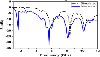
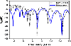
The reflection coefficient ( plot of MCHRMA _ 1 is shown in Fig. 4. The good impedance matching occurs at 5.87 GHz, 8.38 GHz, 10.31 GHz, and 10.95 GHz, with a return loss of -17.89 dB, -24.72 dB, -19.05 dB, and -13.36 dBi. The MCHRMA_1 has an impedance bandwidth of 600 MHz, 360 MHz, 320 MHz, and 740 MHz, respectively. The measured bandwidth is 1790 MHz, 1410 MHz, 1040 MHz, and 1320 MHz, respectively. The measured results have good agreement with the simulated results.
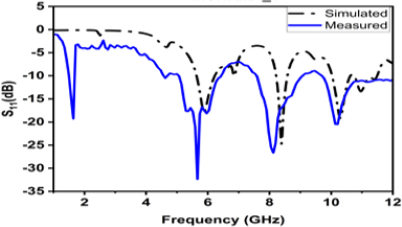
Figure 4: The reflection coefficient plot for MCHRMA_1.
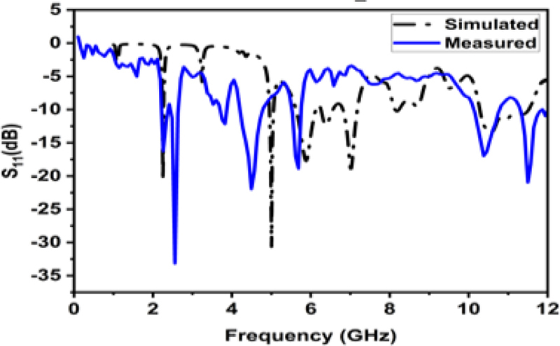
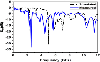
Figure 5: The reflection coefficient plot for MCHRMA_2.
The reflection coefficient (plot of MCHRMA _ 2 is shown in Fig. 5. The good impedance matching occurs at 2.25 GHz, 5 GHz, 5.89 GHz, 6.39 GHz, 7.02 GHz, and 10.57 GHz, with a return loss of -20.68 dB, -30.63 dB, -17.65 dB, -12.34 dB, -18.85 dB, and -13.53 dB. The MCHRMA_2 has an impedance bandwidth of 30 MHz, 110 MHz, 510 MHz, 300 MHz, and 370 MHz, respectively. The measured impedance bandwidths are 80 MHz, 440 MHz, 830 MHz, 520 MHz, 600 MHz, and 1210 MHz. The measured results have good agreement with the simulatedresults.
The reflection coefficient ( plot of MCHRMA _ 3 is shown in Fig. 6. The best impedance matching occurs at 3.79 GHz, 4.85 GHz, 5.39 GHz, 6.09 GHz, 6.98 GHz, 9.32 GHz, 11.03 GHz, and 12.5 GHz, with a return loss of -19.85 dB, -25.16 dB, -11.45 dB, -35.81 dB, -21.91 dB, -10.55 dB, and -34.69 db. The MCHRMA_3 has an impedance bandwidth of 40 MHz, 110 MHz, 340 MHz, 90 MHz, 230 MHz, 250 MHz, 200 MHz, and 1090 MHz, respectively. The measured bandwidth is 150 MHz, 670 MHz, 450 MHz, 450 MHz, 1080 MHz, and 1160 MHz, respectively. The measured results have good agreement with the simulated results. The simulated results are tabulated in Table 3.
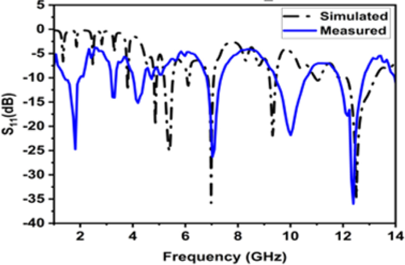
Figure 6: The reflection coefficient plot for MCHRMA_3.
Table 3: Simulated results of MCHRMA up to three iterations
| Antenna Design | (In GHz) | (In GHz) | (In GHz) | BW(In MHz) | (In dB) | Peak Gain(In dB) | Applications |
| MCHRMA_1 | 5.87 | 5.63 | 6.23 | 600 | -17.89 | 4.08 | C-band/WLAN (5.4/5.8 GHz) [10] |
| 8.38 | 8.22 | 8.58 | 360 | -24.72 | 3.41 | Lower X-band/(8.26 GHz) Earth Exploration, satellite services [10] | |
| 10.31 | 10.3 | 10.62 | 320 | -19.05 | 5.08 | X-band/ITU 10 - SHF - Radars, Mobile Phones, and Commercial Wireless LAN | |
| 10.95 | 10.75 | 11.49 | 740 | -13.36 | 4.82 | X-band /ITU 10 - SHF - Radars, Mobile Phones, and Commercial Wireless LAN | |
| MCHRMA_2 | 2.25 | 2.24 | 2.27 | 30 | -20.68 | -14.65 | S-Band /ITU 9- UHF – TV broadcasts,center Bluetooth, GPS, and Two-Way Radios |
| 5 | 4.95 | 5.06 | 110 | -30.63 | -2.01 | C-Band/ITU 10 - SHF - Radars, Mobile Phones, and Commercial Wireless LAN | |
| 5.89 | 5.62 | 6.13 | 510 | -17.65 | 4.69 | C-Band/ITU 10 - SHF - Radars, Mobile Phones, and Commercial Wireless LAN | |
| 6.39 | 6.26 | 6.56 | 300 | -12.34 | 4.37 | C-Band/ITU 10 - SHF - Radars, Mobile Phones, and Commercial Wireless LAN | |
| 7.02 | 6.81 | 7.18 | 370 | -18.85 | 3.5 | C-Band/ITU 10 - SHF - Radars, Mobile Phones, and Commercial Wireless LAN | |
| 10.57 | 10.28 | 11.52 | 1240 | -13.53 | 3.69 | Upper X band(10.48 GHz) Amateur Satellite operating band [10] | |
| MCHRMA_3 | 3.79 | 3.78 | 3.82 | 40 | -12.64 | -5.24 | S-band WiMAX (3.4_3.69 GHz—IEEE 802.16e) [10] |
| 4.85 | 4.8 | 4.91 | 110 | -19.85 | -2.59 | C-Band | |
| 5.39 | 5.19 | 5.53 | 340 | -25.16 | 4.73 | C-Band Wireless LAN (5.5 GHz) [10] | |
| 6.09 | 6.06 | 6.15 | 90 | -11.45 | 2.88 | C-Band | |
| 6.98 | 6.85 | 7.08 | 230 | -35.81 | 0.88 | C-Band | |
| 9.32 | 9.2 | 9.45 | 250 | -21.91 | 2.39 | X-band (ITU 10 - SHF - Radars, Mobile Phones, and Commercial Wireless LAN | |
| 11.03 | 10.93 | 11.13 | 200 | -10.55 | 4.65 | X-band Wireless ISPs (WISP), 4G/5G Operator for LTE Backhaul [10] | |
| 12.5 | 12.14 | 13.23 | 1090 | -34.69 | 5.07 | X-band direct broadcast satellite services |
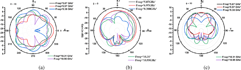
Figure 7: The E-Plane radiation pattern of MCHRMA_1: (a) XZ Plane, (b) YZ Plane, and (c) XY Plane.
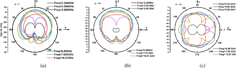
Figure 8: The E-Plane radiation pattern of MCHRMA_2: (a) XZ Plane, (b) YZ Plane, and (c) XY Plane.
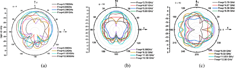
Figure 9: The E-Plane radiation pattern of MCHRMA_3: (a) XZ Plane, (b) YZ Plane, and (c) XY Plane.
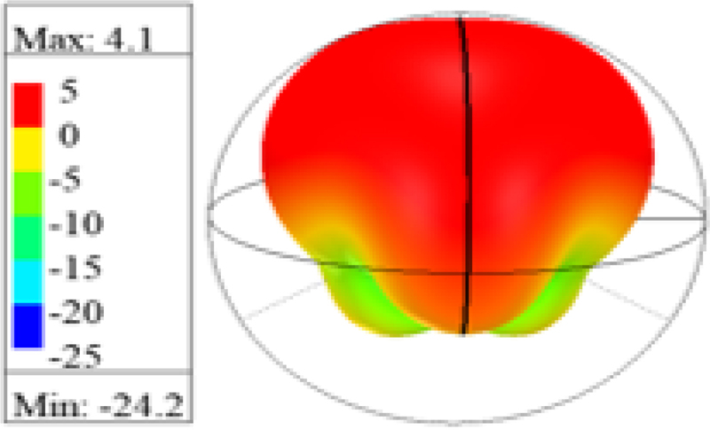
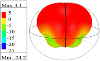
Figure 10: The gain 3D polar plot of MCHRMA_1.
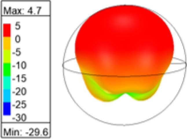
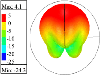
Figure 11: The gain 3D polar plot of MCHRMA_2.
B. Radiation pattern
The radiation pattern of MCHRMA is examined for all its resonance frequencies. The radiation pattern of MCHRMA_1 shown in Fig. 7 has a smooth, stable, and similar response at 5.87, 8.38, and 10.31 GHz. Furthermore, 10.58 GHz patterns have low gain and have ripples in the pattern at the lower hemisphere. The radiation pattern of MCHRMA_2 is shown in Fig. 8. It has a smooth, stable, and similar response at 5, 5.89, 6.39, and 10.97 GHz. Furthermore, 7.02 GHz frequency patterns have low gain and have ripples in the pattern at the lower hemisphere.
The radiation pattern of MCHRMA_3 shown in Fig. 9 has a smooth, stable, and similar response at 5.39, 6.09, 11.03, and 12.5 GHz. Moreover, for 3.79, 4.85, 6.98, 9.32 GHz frequency patterns have low gain and have ripples in the pattern at the lower hemisphere. The radiation pattern has a peak gain of 5.08 dB, 4.69 dB, and 5.07 dB for MCHRMA_1, MCHRMA_2, and MCHRMA_3, respectively.
C. 3D-gain plot
The 3D polar plots for MCHRMA_1, MCHRMA_2, and MCHRMA_3 are shown in Figs. 11, 11, and 12, respectively. The gain plot observed that most radiation is directed over the upper hemisphere, and there is no back radiation. The gain plot has no ripples and side lobes at the resonant frequencies.
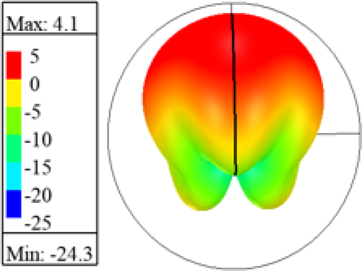
Figure 12: The gain 3D polar plot of MCHRMA_3.
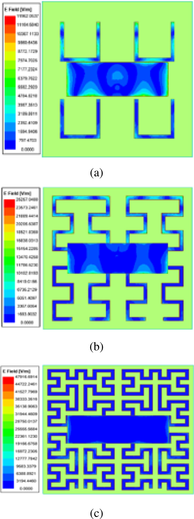
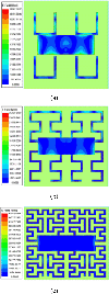
Figure 13: The surface current density plot: (a) MCHRMA_1, (b) MCHRMA_2, and (c) MCHRMA_3.
D. Surface current density
The surface current distribution at various portions of the patch is represented as the surface current distribution. It displays the current density value at different resonance frequencies. The surface current density of MCHRMA_1, MCHRMA_2, and MCHRMA_3 are shown in Fig. 13. Near the feed position, the surface current is more significant and decreases at the edges. It demonstrates that the feed line has the maximum coupling impact, and HIS suppresses the radiation at the edges and improves the broadside gain.
IV. CONCLUSION
The Moore curve-shaped HIS up to three iterations as the ground plane reflector is investigated. The rectangular patch for the WLAN application is designed over the Moore curve. The Moore curve fractal provides a multiband frequency response. When the Moore curve first iteration is used as HIS plane, it has resonant frequencies of 5.87, 8.38, 10.31, and 10.95 GHz, with a peak gain of 3.41 dB to 5.08 dB. With the Moore curvesecond iteration, the HIS plane resonated at frequencies of 2.25, 5, 5.89, 6.39, 7.02, and 10.57 GHz, with a max peak gain of 4.69 dB. Similarly, when the Moore curvethird iteration is used as HIS ground plane, it has resonant frequencies like 3.79, 4.85, 5.39, 6.09, 6.98, 9.32, 11.03, and 12.5 GHz, and a max peak gain of 5.07 dB is achieved. The surface current distribution shows low radiation at the edges, suppresses surface waves, and smoothens the radiation pattern. The antenna has wide applications in the S-band, C-band, and lower X-band operating frequency regime.
REFERENCES
[1] D. F. Sievenpiper, “High impedance electromagnetic surfaces,” Ph.D. dissertation, Dept. Elect. Eng., UCLA, Los Angeles, CA, USA, 1999.
[2] F. Yang and Y. Rahmat-Samii, ”Reflection phase characterization of an electromagnetic band-gap (EBG) surface,” IEEE Antenna Propag. Soci. Int. Symp. (IEEE Cat. No. 02CH37313), San Antonio, TX, USA, pp. 744-747, doi: 10.1109/APS.2002.1018317, 2002.
[3] S. Clavijo, R. E. Diaz, and W. E. McKinzie, “Design methodology for Sievenpiper high-impedance surfaces: An artificial magnetic conductor for positive gain electrically small antennas,” IEEE Trans. Antennas Propag., vol. 51, no. 10, pp. 2678-2690, Oct. 2003.
[4] F. Yang and Y. Rahmat-Samii, “Reflection phase characterizations of the EBG ground plane for low profile wire antenna applications,” IEEE Trans. Antenna Propag., vol. 51, no. 10, pp. 2691-2703, Oct. 2003.
[5] F. Costa, A. Monorchio, S. Talarico, and F. M. Valeri, “An active high-impedance surface for low-profile tunable and steerable antennas,” IEEE Antennas Wireless Propag. Lett., vol. 7, pp. 676-680, Sep. 2008.
[6] D. J. Kern, D. H. Werner, A. Monorchio, L. Lanuzza, and M. J. Wilhelm, “The design synthesis of multiband artificial magnetic conductors using high impedance frequency selective surfaces,” IEEE Trans. Antennas Propag., vol. 53, no. 1, pp. 8-17, Jan. 2005.
[7] M. Hosseini, A. Pirhadi, and M. Hakkak, “Design of a non-uniform high impedance surface for a low profile antenna,” J. Electromagn. Waves Appl., vol. 20, no. 11, pp. 1455-1464, Jan. 2006.
[8] M. Li, S.-Q. Xiao, and B.-Z. Wang, “Investigation of using high impedance surfaces for wide-angle scanning arrays,” IEEE Trans. Antenna Propag. vol. 63, no. 7, pp. 2895-2901, July 2015.
[9] G. Gupta and A. R. Harish, “Circularly polarized antenna using a double layered via-less high impedance surface,” Microw. Opt. Technol. Lett. vol. 58, no. 2, pp. 340-343, Feb. 2016.
[10] P. K. Panda and D. Ghosh, “Wideband bow-tie antenna with increased gain and directivity by using high impedance surface,” Int. J. RF Microw. Comput. Aided Eng., vol. 29, no. 3, pp. e21619, Mar. 2019.
[11] A. T. Almutawa, H. Kazemi, and F. Capolino, “Analyze and design of thin planar high impedance surface as an antenna,” 2018 Int. Conf. Electromag. Adv. Appl. (ICEAA), Cartagena, Colombia, pp. 623-624, doi: 10.1109/ICEAA.2018.8520480, 2018.
[12] G. Cheng, Y.-M. Wu, J.-X. Yin, N. Zhao, T. Qiang, and X. Lv, “Planar Luneburg lens based on the high impedance surface for effective Ku-band wave focusing,” IEEE Access, vol. 6, pp. 16942-16847, Feb. 2018.
[13] M. M. Bait-Suwailam, I. I. Labiano, and A. Alomainy, “Impedance enhancement of textile grounded loop antenna using high-impedance surface (HIS) for healthcare applications,” Sensors, vol. 20, no. 14, p. 3809, July 2020.
[14] J. K. Ali, “A new microstrip-fed printed slot antenna based on Moore space-filling geometry,” 2009 Loughborough Antenna & Propag. Conf., Loughborough, UK, pp. 449-452, doi: 10.1109/LAPC.2009.5352551, 2009.
[15] M. Ali, T. Sittironnarit, V. K. Kunda, H. S. Hwang, R. A. Sadler, and G. J. Hayes, “Wideband patch antenna for 5-6 GHz WLAN applications,” IEEE Antennas and Propag. Society Int. Symp. Digest, Columbus, OH, USA, pp. 930-933, vol. 2, doi: 10.1109/APS.2003.1219387, 2003.
[16] J. Anguera, A. Andújar, J. Jayasinghe, V. V. S. S. S. Chakravarthy, P. S. R. Chowdary, J. L. Pijoan, T. Ali, and C. Cattani, “Fractal antennas: An historical perspective,” Fractal and Fractional, vol. 4, no. 1, p. 3, Jan. 2020.
BIOGRAPHIES

Akash K. Gupta received the B.Tech. and M.Tech. degrees from Jawaharlal Nehru Technological University, Kakinada, India, in Electronics and Communication Engineering in 2011 and 2013, respectively. Since 2019 he has been a student researcher in antenna engineering at Centurion University of Technology and Management, Odisha, India. His research interests include microstrip antenna, electromagnetic band-gap structures, high impedance surface antenna designs, and embedded systems.

Paladuga S. R. Chowdary is a Professor and Vice Principal at Raghu Institute of Technology, Visakhapatnam, India. He obtained the M.Tech. and Ph.D. degrees from Andhra University, Visakhapatnam, and Jawaharlal Nehru Technological University, Kakinada, India, respectively. He has been teaching for 20 years and has 5 years of research experience. His research interests are evolutionary computing tools, computational electromagnetics, fractal antennas, and image processing. He is a Senior Member of the IEEE, the Applied Computational Electromagnetics Society, a Life Member of the Instrument Society of India (ISOI), the International Computer Science and Engineering Society (ICSES), and the Soft Computing Research Society (SCRS).

Mandhapati V. Krishna obtained the Ph.D. degree in Computational Electromagnetics and Antennas from Centurion University, Odisha, India, the M.Tech. degree in Radar and Microwave Engineering from Andhra University, Visakhapatnam, and the B.Tech. degree from Biju Patnaik University of Technology, Odisha. His research interests include soft computing, evolutionary computing tools, antennas, and electromagnetic systems. He is currently a Professor and Head of the Department of Electronics and Communication Engineering, Dhanekula Institute of Engineering and Technology, Vijayawada, Andhra Pradesh, India.
ACES JOURNAL, Vol. 38, No. 6, 392–399
doi: 10.13052/2023.ACES.J.380603
© 2023 River Publishers