A Compact Wideband Branch Line Coupler for Lower 5G Applications
Balasem S. Samet and Ahmed A. Abbas
Department of Electrical Engineering
Faculty of Engineering, University of Anbar, Anbar, Iraq
balasem.sumait@uoanbar.edu.iq, Ahmed.abbas@uoanbar.edu.iq
Submitted On: December 28, 2022; Accepted On: May 19, 2024
ABSTRACT
This paper presents a new design approach of a compact wideband branch line coupler based on waveguide technique at 3.5 GHz. At the lower band of 5G technology, microwave devices such as hybrid couplers tend to be narrower in bandwidth and big in size, in addition to the phase difference error produced by using common planar technology. Therefore, waveguide technology aims to solve those challenges. This work aims to design a compact wideband coupler by implementing a direct coupling aperture between two waveguides with a cutting in the narrow wall of the structure. This technique helps in obtaining a wide bandwidth and reduces the size of the whole structure. The coupler is simulated using computer software technology and fabricated using CNC machining. The measured S-parameters of the coupler are observed to have low loss properties with return loss and isolation less than 10 dB. The coupling factor at the outputs are 3.21 dB with low loss of 0.2 dB. The measured phase error is about 2 at 3.5 GHz. A size reduction of 70% is observed compared to conventional waveguides and planar couplers. Overall, this coupler shows great performance that could be used for 5G beamforming applications.
Index Terms: 5G, branch line coupler, compact size, direct coupling, waveguide.
I. INTRODUCTION
Hybrid couplers, better known as branch line couplers (BLCs), are widely implemented in microwave and millimeterwave devices specifically for beamforming network and antenna array systems [1–3]. Hybrid couplers play significant component roles in designing accurate antenna beamforming systems. This is due to its importance in controlling the output power and the phase difference for such complex systems [2]. Generally, a hybrid coupler is a two-port network with two inputs and two outputs. It acts as a power divider which equally splits the input power at the outputs with a phase difference of 90 or 180 [3]. As one of the inputs is excited, the outputs receive an equal magnitude of 3 dB with different phase of 90 between the output ports. However, hybrid couplers are popularly known for their narrow bandwidth properties [4]. In addition, at lower frequency the size occupied by the planar couplers is quite big and unfixable. Hence, various methods and techniques are presented to enhance the coupler bandwidth and the size by introducing waveguide and substrate integrated waveguide technologies [5–7].
Waveguide couplers are usually presented in the high frequency bands [8]. This is due to the small size and high coupling that could be obtained in such frequencies. Yet, few attempts have been done to implement the waveguide structure in the coupler design at lower bands (lower than 10 GHz). For example, a directional waveguide coupler is designed from 7.7 GHz to 12 GHz using coupling of two rectangular waveguides by [9]. A good return loss and isolation are obtained of less than 20 dB. However, the size of the coupler is not suitable for further beamforming implementation. Another waveguide coupler at X-band is introduced by [10]. The coupler is designed using a single waveguide structure with slots cut in the broad wall of the waveguide structure. The obtained results showed a good performance at 10 GHz, with a size reduction of 44% and FBW of 50%. As a result, this work aims to present a first attempt to design a waveguide coupler using two waveguides with modified narrow walls and a coupling aperture between them at a lower band of 5G (sub-6 GHz).
The contribution of this paper is summarized in two major points. First, modification of the narrow wall of the waveguide to reduce the size at 3.5 GHz by more than 70%. Second, provide a high-performance coupler compared to the existing ones with different planar technology at the same frequency. Section II presents the design method. Section III discusses the results. Section IV summaries the paper.
II. DESIGN OF COUPLER
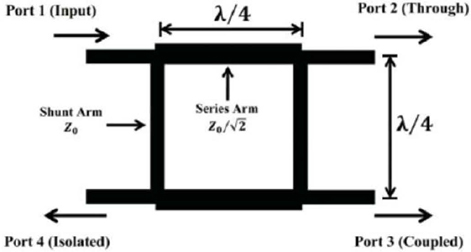
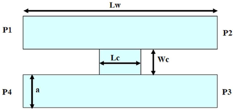
Figure 1 shows the common hybrid coupler structure with four ports implementation. The input port (port 1) is the return loss port denoted as . The isolation port (port 4) is the port that blocks the signal and denoted as . The through port (port 2) and the coupling port (port 3) are the output ports and named as and , respectively [11, 12]. The hybrid coupler is designed with four branches with quarter wavelength transmission lines in which the input impedance is equal to 50 . To convert this hybrid coupler into a waveguide structure form, two rectangular waveguides replace two branches. The coupling branch is replaced with a coupling waveguide aperture placed in the middle of the two rectangular waveguides as illustratedin Fig. 2.
Figure 1: The common hybrid coupler structure.
Figure 2: The waveguide structure replacement of the hybrid coupler in Fig. 1. (Lw length of section, Wc width of coupled section, Lc coupling area, P1 input port, P2 output port, P3 coupling port, P4 isolation port).
The first step is to calculate the guided wavelength and the cut-off frequency of the waveguide structure. This could be found by [13]:
| (1) |
| (2) |
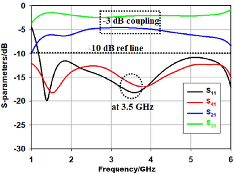
where the waveguide is air-filled with permittivity () and permeability (), the mode of of m and n, and as waveguide inner dimensions, and is the desired wavelength. At 3.5 GHz, the initial dimensions of the waveguide coupler are: ). The conventional coupler is simulated in order to analyze its S-parameters as shown in Fig. 3. The performance of the return loss and the isolation at 3.5 GHz show good values below 10 dB with , whereas the outputs power varies from 3.5 dB at port 2 to 4.8 dB at port 3. As a result, the coupler is operated at its minimalrequirements.
Figure 3: S-parameters of the conventional waveguidecoupler.
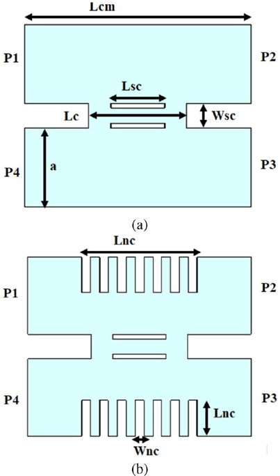
The second step is to modify the coupler in order to reduce the size and match the output powers to have equally split a 3 dB coupling. Figure 4 (a) shows the coupler modification by adding two aperture slot couplings to the middle aperture. This technique enhances the S-parameters of the coupler. Figure 4 (b) demonstrates the adding of slot cutting arms in the narrow wall of the two waveguides. This method is used to reduce the size of the two rectangular waveguides and improve the output powers at port 2 and port 3.
Figure 4: The proposed waveguide coupler. (a) Two slots coupling apertures (Lcm waveguide length, Lc coupling length, Wsc width of coupling, Lc coupling area length) and (b) waveguide narrow wall modified with arms coupling apertures (Lnc arm length, P1 port 1, P2 port 2, P3 port 3, P4 port 4).
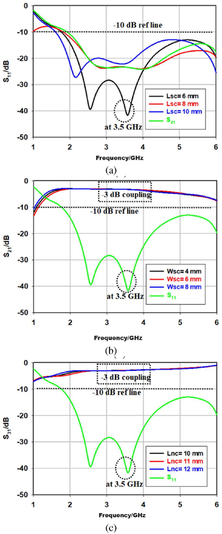
To analyze the performance of the modified coupler, a parametric study on the length () and the width () of the two slots coupling aperture with arms coupling length () is done with the aid of CST 3D model software as shown in Fig. 5.
Figure 5: S-parameters parametric study of the proposed coupler. (a) Return loss with respect to the length of coupling aperture, (b) through power with respect to the width of coupling aperture, and (c) coupling with respect to the length of arms.
From Fig. 5 (a), the length of the coupling slot apertures affects the return loss in that it increases and shifts the value of the return loss and the frequency, respectively. As decreases, the return loss increases to be 41 dB and shifts to 3.5 GHz. Hence, at , the bandwidth is more than 2 GHz and the isolation is below 20 dB. The width of the coupling slot apertures can be varied in order to achieve a perfect 3 dB through power at port 2 as seen in Fig. 5 (b). As increases the through power tends to be 3 dB and return loss remains unchanged. Hence, the optimal value for the width of the coupling aperture is 8 mm. Finally, the coupling power at port 3 increases as the arms coupling length increases as shown in Fig. 5 (c). Hence, the optimal value for the arms coupling length in the waveguide narrow wallis 12 mm.
As all the dimensions of the proposed coupler are obtained from the parametric study and the S-parameters performance, the final dimension for the proposed coupler are as follows: .
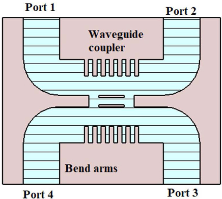
Figure 6 shows the final structure for the proposed coupler for the fabrication process. The structure has been added with four additional arms bent to make the measurements possible. The four ports couplers are attached with waveguide adaptors in order to measure the amplitudes and the phases.
Figure 6: The final structure of the proposed coupler.
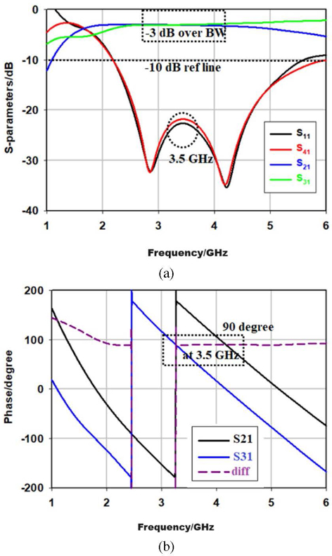
The optimized coupler performance is plotted in Fig. 7 in terms of S-parameters and phases. A fractal bandwidth of 97% is obtained with equal power split of 3 dB over the bandwidth. A 90 phase difference at 3.5 GHz is also achieved at the output ports.
Figure 7: (a) S-parameter responses of the proposed coupler and (b) phases of the outputs.
III. RESULTS AND DISCUSSION
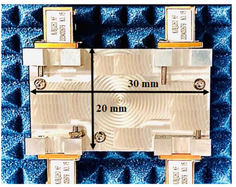
The coupler is fabricated using a metal plate of aluminum by CNC machining with depth of cut of 0.6 mm, feed rate of 0.2 mm, and cutting speed of 3500 rpm. Figure 8 shows the fabricated prototype with total dimensions of 30 mm 20 mm. The prototype highlighted a small size compared to the conventional coupler (waveguide) of 80 mm 40 mm with a size reduction of 89%.
Figure 8: The coupler prototype.
The S-parameter measurements are done as follows. First, terminator loads are connected at port 2, port 3, and port 4, respectively. Then, port 1 is connected with a measurement cable of a standard vector network analyzer (VNA) port 1 to measure the return loss (). Second, remove the terminator load at port 2 and connect it to the measurement output cable of VNA port 2. This step is to measure the output power at port 2. The same procedure is repeated for port 3 and port 4 whilst port 1 is still connected to the input port of the VNA. This allows us to measure the coupling and isolation at port 3 and port 4. The measurement process includes the results in the form of magnitude and phase at all ports. Slight loss can occur due to cable loss and mismatched port connections.
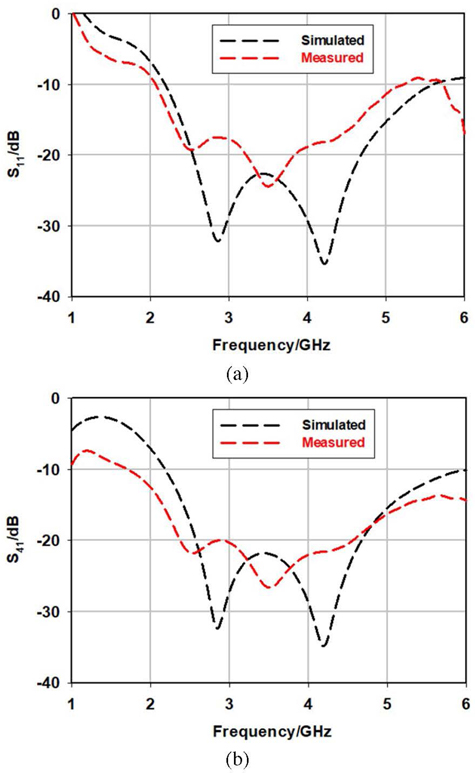
Figure 9 illustrates the measured responses of the fabricated coupler in terms of the input and isolation ports. The input port has a measured bandwidth of 3.22 GHz ranging from 2.1 GHz to 5.32 GHz with a peak return loss of 23.78 dB at 3.5 GHz at shown in Fig. 9 (a). The isolation value over the bandwidth is less than 10 dB as seen in Fig. 9 (b). Hence, low loss properties are achieved compared with the simulated results.
Figure 9: Comparison of (a) return loss and (b) isolation of the coupler.
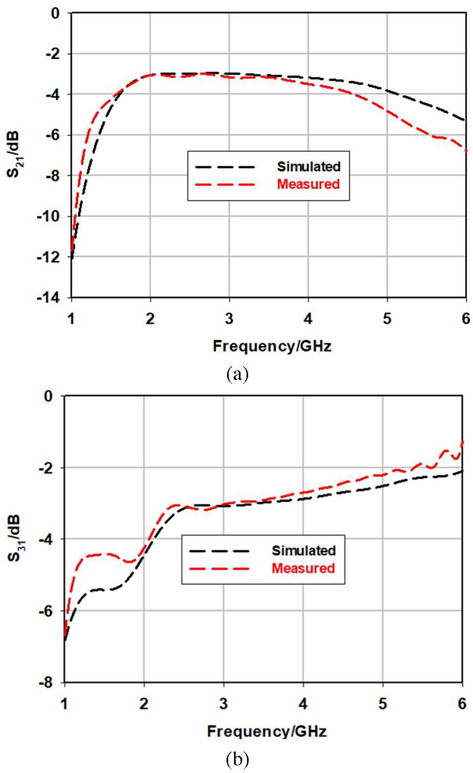
Figures 10 (a) and (b) show the through and coupling measured performances at output port 2 and port 3, respectively. The measured port 2 power is 3.12 dB compared to the simulated power of 3.05 dB. Similar results are obtained at output port 3 with a measured power of 3.16 dB compared to the simulated one of 3.22 dB. This indicates a low loss is achieved with 0.1 dB error.
Figure 10: Comparison of (a) through power and (b) coupling of the coupler.
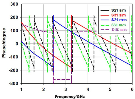
Figure 11: Comparison of the phases of the coupler at port 2 and port 3.
Figure 11 plots the measured phases of port 2 and port 3 with the phase differences at these output ports. It is clearly seen that the measured phases along with the phase difference agreed well with the simulated phases. The phase error is very low with a value of 2. Table 1 compares the measured and the simulated responses of the proposed coupler. Comparison between the performances of the fabricated prototype with respect to other existing work in shown in Table 2. The comparison shows that the proposed coupler has better bandwidth, low loss, low phase difference error, and size reduction among other designs. Overall, it is proven that using this waveguide coupler with the coupling slot structure and arms coupling slot in the narrow wall could work well in reducing the size and maintaining the sameperformance.
Table 1: Measured and simulated responses of the proposed coupler at 3.5 GHz
| Parameters | Simulated | Measured |
|---|---|---|
| 23.52 dB | 23.78 dB | |
| 3.05 dB | 3.12 dB | |
| 3.22 dB | 3.16 dB | |
| 22.5 dB | 25.4 dB | |
| Bandwidth | 3.4 GHz | 3.22 GHz |
| Phase Diff. | 90 | 88 |
Table 2: Comparison of other related works with the proposed coupler
| Ref | Method | Freq. (GHz) | BW (GHz) | Size % | Phase error () |
| [3] | Microstrip | 3.5 | 2.3 | 25 | 5.6 |
| [4] | Microstrip | 3.5 | 1.9 | 34 | 7.2 |
| [10] | Waveguide | 10 | 2 | 15 | 6 |
| [11] | Waveguide | 20 | 5 | 10 | 11 |
| [12] | Waveguide | 12 | 4.3 | 18 | 8 |
| [13] | SIW | 8.8 | 4 | 20 | 4.6 |
| This work | Waveguide | 3.5 | 3.22 | 89 | 2 |
IV. CONCLUSION
This paper proposes a new method of designing a waveguide hybrid coupler at lower bands of 5G technology. The designed waveguide hybrid coupler is implemented with two coupling aperture slots and arms waveguide coupled structure in the narrow wall. The performance of the coupler showed a size reduction of 89% and a bandwidth of 3.22 GHz. The coupler has low loss properties in terms of S-parameter and phase difference with 0.1 dB loss and 2 phase error. Hence, this coupler is a good candidate for future 5Gapplications.
REFERENCES
[1] M. Almeshehe, N. Murad, M. Rahim, O. Ayop, N. Samsuri, M. Aziz, and M. Osman, “Surface roughness impact on the performance of the 3D metal printed waveguide coupler at millimeterwave band,” Engineering Science and Technology, an International Journal, vol. 35, pp. 129-139,2022.
[2] R. Dehdasht-Heydari, K. Forooraghi, and M. Naser-Moghadasi, “Efficient and accurate analysis of a substrate integrated waveguide (SIW) rat-race coupler excited by four U-shape slot-coupled transitions,” Applied Computational Electromagnetics Society (ACES) Journal, vol. 30, no. 1, pp. 42-49, 2015.
[3] N. Shukor, N. Seman, and T. Abd Rahman, “Wideband multi-port network integrated by 3-dB branch-line couplers,” Applied Computational Electromagnetics Society (ACES) Journal, vol. 33, no. 7, pp. 764-771, 2018.
[4] A. Bekasiewicz, “Miniaturized dual-band branch-line coupler with enhanced bandwidth,” Microwave and Optical Technology Letters, vol. 61, no. 6, pp. 1441-1444, 2019.
[5] A. K. Vallappil, M. K. A. Rahim, B. A. Khawaja, and M. Aminu-Baba, “Metamaterial based compact branch-line coupler with enhanced bandwidth for use in 5G applications,” Applied Computational Electromagnetics Society (ACES) Journal, vol. 35, no. 6, pp. 700-708, 2020.
[6] Z. Mansouri, M. Kishihara, F. B. Zarrabi, and F. Geran, “Modified broadband half mode substrate integrated waveguide cruciform coupler,” Applied Computational Electromagnetics Society (ACES) Journal, vol. 29, no. 11, pp. 881-886, Aug.2021.
[7] T. Yasui, J.-I. Sugisaka, and K. Hirayama, “Structural optimization of an optical 90 degree hybrid based on a weakly guided 4x4 multimode interference coupler using a parallelized real-coded micro-genetic algorithm,” Applied Computational Electromagnetics Society (ACES) Journal, vol. 36, no. 05, pp. 526-532, July 2021.
[8] A. A. Abbas and B. S. Samet, “A compact high gain wideband metamaterial antenna for sub-6 GHz applications,” Applied Computational Electromagnetics Society (ACES) Journal, vol. 37, no. 08, pp. 886-892, Jan. 2023.
[9] Z. Mousavirazi, M. M. M. Ali, H. N. Gheisanab, and T. A. Denidni, “Analysis and design of ultra-wideband PRGW hybrid coupler using PEC/PMC waveguide model,” Scientific Reports, vol. 12, no. 1, pp. 2-15, 2022.
[10] G. Simoncini, R. Rossi, F. Alimenti, and R. Vincenti Gatti, “Single-ridge waveguide compact and wideband hybrid couplers for X/Ku-band applications,” Electronics, vol. 11, no. 10, pp. 1538-1550, 2022.
[11] D. Sun and J. Xu, “Rectangular waveguide coupler with adjustable coupling coefficient using gap waveguide technology,” Electronics Letters, vol. 53, no. 3, pp. 167-169, Feb. 2017.
[12] J. Ma, “A highly directional eight-hole coupling circular waveguide coupler,” International Journal of RF and Microwave Computer-Aided Engineering, vol. 32, no. 8, 2022.
[13] Z. Zhang, Y. Fan, and Y. Zhang, “Multilayer half-mode substrate integrated waveguide wideband coupler with high selectivity,” Applied Computational Electromagnetics Society (ACES) Journal, vol. 34, no. 9, pp. 1418-1425, 2019.
BIOGRAPHIES

Balasem Salem Samet is lecturer in Electrical Engineering Department, College of Engineering, and University of Anbar. He received the B.Sc. degree in Electrical Engineering/University of Technology in 2000, he received M.Sc. in communication Engineering /University of Technology in 2005 and he received Ph.D. in communication Engineering in 2013. Dr. Balasem is researcher in wireless communication and smart antenna.

Ahmed A. Abbas is a head of Electrical Engineering Department, College of Engineering, University of Anbar from 2018 till now. He received the B.Sc. degree in Electrical Engineering/University of Technology in 1994, he received M.Sc. in communication Engineering /University of Technology in 2005 and he received Ph.D. in communication Engineering/Ankara Yldrm Beyazt University in 2017. Dr. Ahmed is researcher in communication field especially in optical wave propagation through random media.
ACES JOURNAL, Vol. 39, No. 4, 334–340
doi: 10.13052/2024.ACES.J.390407
© 2024 River Publishers
