Analytical Solution of Eddy Current in Parallel Conducting Strips for Low-frequency Shielding Purposes
Hamzeh M. Jaradat, Qasem M. Qananwah, Ahmad M. Dagamseh, and Qasem M. Al-Zoubi
1Department of Telecommunications Engineering, Hijjawi Faculty for Engineering Technology
Yarmouk University, Irbid, P.O. Box 21163, Jordan
hamzehjaradat@yu.edu.jo
2Department of Biomedical Systems and Informatics Engineering, Hijjawi Faculty for Engineering Technology
Yarmouk University, Irbid, P.O. Box 21163, Jordan
qasem.qananwah@yu.edu.jo
3Department of Electronics Engineering, Hijjawi Faculty for Engineering Technology
Yarmouk University, Irbid, P.O. Box 21163, Jordan
a.m.k.dagamseh@yu.edu.jo, qzabi50@yu.edu.jo
Submitted On: January 16, 2023; Accepted On: September 22, 2023
ABSTRACT
In instrumentation systems, shielding is the main issue that judges the performance of the system. The electromagnetic (EM) noise may affect the performance of the instrumentation system if inadequate protection is reached. It is considered the main source of unprotectable interference that may affect these systems in many cases. In this paper, shielding is attained by wrapping the source carrying signal with periodic thin conductive strips separated by slots or openings. This arrangement will protect the sources from the outside EM fields. Shielding factor and shielding efficiency are studied by extracting magnetic fields. For this purpose, an analytical solution based on solving Laplace’s equation for the magnetic vector potential in the region of interest is presented. A closed form of the induced eddy current in the conductive strips is calculated based on Fourier series expansion. Furthermore, numerical simulation using the commercial software MWS CST is employed to validate the analytical solution. The performance of the proposed shielding structure is studied and analyzed in terms of shielding factor and shielding efficiency. The outcomes of both methods are showing very good agreement.
Index Terms: Eddy current, electromagnetic (EM) shielding, quasistatic, shielding efficiency, shielding factor.
I. INTRODUCTION
Electromagnetic Interference (EMI) resulting from EM fields is the most effective interference that may deviate the instrumentation system performance. The evolved system requirements to overcome the inaccuracy and measurement errors through reducing EMI and producing free-of-noise signals have all been thoroughly considered. EMI has been handled to make the electronic system immune to measurement inaccuracy and errors. Electromagnetic shielding (EMS) is typically used to block or minimize either the emitted or reflected electromagnetic fields, which is the most effective way to reduce EMI. Shielding can ensure better isolation depending on the shielding structure or shape. The performance of magnetic shielding was proposed by Kim et al. [1]. An excellent shielding factor was obtained when double-layer shielding using inner silicon steel layer and mu-metal outer layer. Various shielding strategies have been investigated in the literature. Multilayer shielding was proposed in [2] and [3], where numerical analysis for shielding efficiency was calculated. The effect of material properties on the magnetic shielding was further investigated in [4] using different electrical steel panels. Park et al. [5] proposed a shielding structure that comprises a periodic metal strip inserted on a conventional ferrite plate. The model was studied by exploring the effect of metal strips on shielding properties. This shielding technique with strips has found many real-life applications [6]. Magnetic shielding of cylindrical geometry was studied and analyzed [7], [8]. The analysis deduced an inherent relationship between shielding efficiency and shielding parametersinvolved.
Due to the presence of a time-varying magnetic field, the mechanism of shielding arises from the fields’ cancellation, which is determined by the induced eddy current in the shield material. Several methods have been reported to find a general solution of eddy current in conductors analytically and numerically. The solution method depends on the geometry and excitation type. Closed-form expressions for eddy current in cylindrical shielding structures are obtained using second-order vector potentials [9]. The modified Bessel and exponential functions [10] are exploited to calculate the eddy current field excited by a probe coil near a conductive pipe [11]. Eddy current in conducting plates was found through solving the vector potential as a series of eigenfunctions [12]. Reduced vector potential combined with Dirichlet-to-Neumann boundary conditions, was proposed to predict the induced current density distribution in nondestructive testing applications [13]. Computational numerical techniques such as finite element method (FEM) [14] and finite difference method (FDTD) [15] were utilized to calculate the induced eddy currents in thin metal sheets. These methods are complicated and require a dense system matrix. The quasi-static approximation is applied to Ampere’s law, where the total magnetic field is characterized by excited and induced fields. The resulting Laplace equation was solved analytically for many practical geometries [16]. In this paper, a model of periodic coplanar conductive strips is developed. Eddy current is obtained analytically by solving the Laplace equation combined with Fourier series expansion. The effect of the strip’s shielding parameters is investigated analytically and numerically.
II. EDDY CURRENT ANALYTICAL SOLUTION
The geometry comprises very thin, infinitely long parallel conductive strips of width and thickness that are extending along the -axis. The strips are placed periodically along the -direction on the -plane (i.e., parallel conductive strips). The slit width between the adjacent strips is . The source of the exciting field is created using an infinite number of conductive lines separated by a distance that are arranged periodically at plane in parallel with the strips. The currents are distributed in an alternating fashion such that every two lines with different polarities are positioned on the top of each strip. Such configuration creates an alternating magnetic field. The arrangement of the geometry is illustrated in Fig. 1.
According to Faraday’s law of induction, the time-varying magnetic fields generate an induced conduction eddy current in the conductive strips. As a response, this current creates a magnetic field that opposes the change in the excitation field. To find the eddy currents, the general solution for the vector potential should be determined. Because the system is periodic in the -direction with a period of , the exciting vector potential due to line currents can be presented as the sum of solutions of the two-dimensional Laplace equation for quasistatic fields [17].
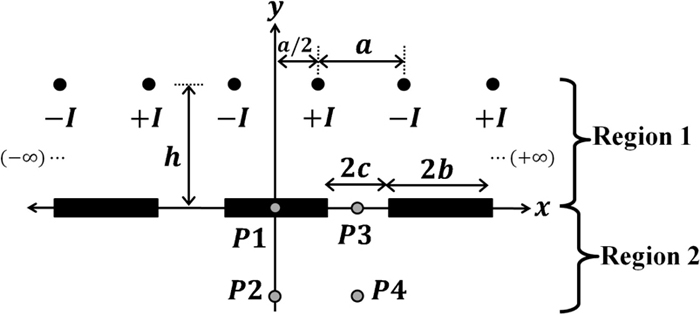
Figure 1: Geometry of the proposed shielding system.
| (1) |
The general solution for (1) is performed using the separation of variables technique, i.e., . It is noted that the magnetic vector potential has only the -component. Therefore, the vector potential of the known currents in the lines can be written as
| (2) |
where and are the magnetic vector potentials in the regions above and below the lines, respectively, is the magnetic permeability of the medium, and is a positive integer. Similarly, the vector potential due to the eddy currents in the conducting strips can be determined by solving the Laplace equation under symmetry conditions. The vector potential solution due to the unknown eddy currents becomes
| (3) |
where and are the magnetic vector potentials in the regions above and below the conductive strips respectively, are unknown coefficients that are yet to be determined. The solution is required in the two regions: region 1, and region 2, as depicted in Fig. 1. The complete solution is formulated by combining (2) and (3) [16]:
| (4) |
Boundary conditions should be applied at both regions with,
| (5) |
| (6) |
where , , , and are the magnetic vector potentials and tangential magnetic fields above and below the shielding surface, respectively. The magnetic field intensity is related to the vector potential by the formula . From (6), the surface current density can be written as:
| (7) |
The eddy current flows only inside the strips such that the surface current density at can be determined using the law of induction inside the lateral conducting strips:
| (8-a) |
| (8-b) |
| (8-c) |
where is the conductivity function of the strips, which is considered as a periodic function with a constant magnitude and a period of . Consequently, it can be rewritten in terms of a Fourier series expansion:
| (9) |
Equating the current density expression in (7) with (8) and conducting some mathematical manipulations, will end up with a system of an infinite number of linear equations as in (10-a). The unknown coefficients can be calculated by constructing the matrix elements in (10-b) and (10-c).
| (10-a) |
| (10-b) |
| (10-c) |
where is the skin depth. For the numerical solution, the maximum value of the magnetic field is observed at specific points labeled and . The positions of and are in the same plane of the strips, while and are located underneath the strips as indicated in Fig. 1. Only the y-component of the magnetic field is exited at these points, which can be calculated from (4) using the relation. For instance, the flux density at and can be written as
| (11-a) |
| (11-b) |
The magnetic flux without shielding strips, which is only due to the source currents, can be found from (2) in all regions. At points and , the fields become
| (12-a) | ||||
| (12-b) |
Based on the previous analysis, the shielding factor can be defined as the ratio of the induced magnetic field without conductive strips to the induced magnetic field in the presence of conductive strips [18]. At points and the shielding factor in dB becomes
| (13) |
The maximum shielding occurs when there is no gap between the strips, which means a continuous conductive plane. The induced magnetic fields in the presence of the plane at the two observation points and become
| (14) |
The performance of the field’s isolation is characterized by the shielding efficiency (). It can be defined as the ratio of the induced magnetic field with conductive strips to the induced magnetic field in the presence of a continuous conductive plane.
| (15) |
III. RESULTS AND DISCUSSION
The theoretical analysis conducted in the previous section will be applied to obtain the shielding factor and efficiency at some predefined points ( and , see Fig. 1). The shielding effectiveness has been considered through the shielding factor. The effect of various design parameters has been investigated. These design parameters include the position of the excitation current source relative to the width of the strip (i.e., ), slot size, and excitation frequency. Moreover, the presented analytical results are verified using numerical simulations with the aid of the commercial simulation package MWS CST [19]. The simulation setup is carried out through a low-frequency solver. This solver is a 3D solver used for simulating the time-harmonic behavior in low-frequency systems. The simulated structure is composed of two parallel cylindrical lines, each of which has a diameter of 0.2 cm and a separation distance cm. The two lines are excited using path current sources with equal currents and out of phase. The conductive shielding strip is placed beneath and in parallel with the line currents at a distance of . The strip has a width of and thickness of cm. The length of both current lines and the strip is cm. All conductors are modeled by copper with a conductivity of S/m. This structure has infinite periodicity along the -direction and infinite extent along the -direction. Therefore, to simulate this type of structure, a unit cell of finite length could be simulated by choosing proper boundary conditions. Due to the symmetrical geometry along the -direction, periodic boundary condition is chosen to mimic infinite copies of the unit cell (i.e., at ). On the other hand, the structure has infinite extent in the -direction, which yields at . Open boundaries are defined along -directions. Tetrahedral meshing technique is utilized to perform the computational simulation in the frequency range of 10 Hz to 3 kHz, which is chosen as an illustration example to validate the presented analytical solution. All simulation data are calculated with the aid of field monitors combined with a post-processing template to process the obtained data.
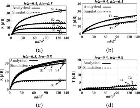
Figure 2: Shielding factor “S” at (a) , (c) and shielding efficiency “T” at (b) and (d) for different observations points as a function of .
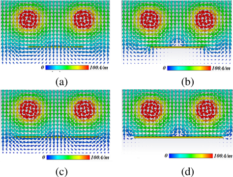
Figure 3: 2D H-field maps for at (a) , (b) , and for at (c) and (d) .
In Fig. 2, the shielding factor S in dB is plotted versus the ratio at four observation points, where this ratio maps to the operating frequency. Both analytical solutions using (13) and simulated responses are plotted together in Fig. 2 (a) for height and strip width . The improvement of the shielding factor is noticed as the frequency increases, and it reaches a steady level at high-frequency values. This trend is noted at all observation points. The highest shielding level occurs at the center of the shield directly underneath the conducting strip at the conductor-air interface. The thickness of the shielding strip is insignificant compared to wavelength . Therefore, the magnetic field’s strength at this position is approximately equal to the field’s strength at the center of the strip indicated by point . At low frequencies, the magnetic field can penetrate the shielding strip, where its thickness is smaller than the skin depth . Therefore, the shielding factor shows low values. This phenomenon is observed from the 2D magnetic field vector maps shown in Fig. 3 (a) for . The magnetic field is transmitted through the conductive strips, since the induced eddy current is small. Increasing the excitation frequency, the shielding factor improves drastically (see Fig. 3 (b) for ). This is due to the effect of surface-induced eddy current, which cancels out the magnetic field at the strip surface. Therefore, the magnetic field penetration in the vicinity of the strips decreases significantly. From (7), the real and imaginary parts of the normalized induced current density on the strips at can be evaluated using (16-a) and (16-b), which are plotted in Fig. 4 (a):
where the constant . It can be seen from this figure that the current density has a comparable imaginary part with the real part. Therefore, the induced magnetic field due to eddy current is not enough to cancel out the source’s field. When increasing the frequency, the shielding factor improves. It is maintained above 30 dB at higher frequencies; i.e., .
Less shieldingis observed of 15 dB at a distance below the strip at point , which is indicated by the curve . As expected, poor shielding performance is observed in the slot and the region below the slot, as can be deduced from and curves at and , respectively. The steady-state shielding factor at these two points is 3 and 9 dB, respectively. The 2D H-field map shown in Fig. 3 (b) illustrates the major reduction of the field’s strength in the region below the strip. Whereas the field’s strength is maintained high in the slot region, the field’s cancelation is due to the increase in an eddy current field manifested by the increase in the current density’s real part, as depicted in Fig. 4 (b). The shielding efficiency is also compared, where the analytical solution using (15) and the simulated response are both plotted in Fig. 2 (b) for height and strip width . Higher shielding efficiency is realized in the region directly below the conductive strips compared with the region below the slots, where 0 dB reference resembles the ideal value. This can be deduced from the curves labeled T2 and T4, which correspond to the fields observed at positions and , respectively.
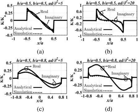
Figure 4: Normalized surface current density “” at for strip width at (a) , (b) and at (c) and (d) as a function of normalized position .
As expected, shielding factor improves drastically by increasing the strip’s width (i.e., reducing the slot’s size), especially at positions and . The shielding factor has enhanced to 26 dB and 28 dB respectively at (see Fig. 2 (c), which shows the responses at all observation points for strip’s width and fixed height ). Similarly, the shielding efficiency also improves as illustrated in Fig. 2 (d). The response approaches the 0 dB level and gets closer to the shielding performance of the continuous sheet. The 2D map of magnetic field vector at low frequency is shown in Fig. 3 (c), while the field map at a higher frequency is depicted in Fig. 3 (d). The field’s reduction in the region under the strips is obvious due to the induced field originating from an increasing eddy current that counterparts the original field. The current density is plotted in Figs. 4 (c) and (d) at low and high frequencies, respectively. Again, the real part of the surface current density is reduced significantly with respect to the real part at higher frequencies compared with the case of low frequencies. Further inspection is conducted by studying the effect of the strip’s width on the shielding factor and efficiency at fixed height . Figure 5 shows the calculated and simulated responses of S and T at different observation positions for and respectively. The shielding factor at high frequency shown in Fig. 5 (a) reveals the behavior of increasing the normalized strip’s width from 0 to 1.
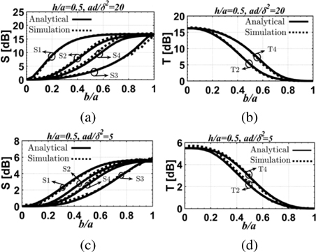
Figure 5: Shielding factor “S” at (a) , (c) and shielding efficiency “T” at (b) and (d) for different observation points as a function of normalized strip width .
The zero-width corresponds to no shielding and the unity value corresponds to continuous plane shielding. The shielding factor approaches the maximum value of 15 dB when exceeds . Therefore, the performance of the shielding system behaves similarly to the continuous plane, especially in the region below and away from the conductive strips as indicated in the curves , , and . Poor shielding is expected at the gap between the strips as indicated in the S3 curve. This is also seen from the T curves in Fig. 5 (b), where the efficiency is approaching the 0 dB level for . The low-frequency performance is depicted in Figs. 5 (c) and (d) for S and T, respectively. The trend of increasing b is very similar to the case of high frequency but with a less efficient shielding level.
The excitation source of the parallel current lines has an insignificant impact on shielding performance, as revealed from studying the variation of the parameter , which is swept in the range 0.1-2. The strip’s width is kept fixed at . Figure 6 (a) shows the response of S at the four observations points for . The shielding factor is almost constant with the height variation. Since the excitation source position with respect to the strips only determines the magnetic field’s strength, the shielding factor is not affected by increasing the source’s height. The change of the H-field with the absence of the strips is equal to the change of the field with the exitance of the shielding strips. Therefore, the ratio of the fields remains steady. This can be observed also even with different operating frequencies, as seen in Fig. 5 (c), where the value of is 5. The flat response of the shielding efficiency T is also attained in Figs. 6 (b) and (d) at high and low frequencies, respectively.
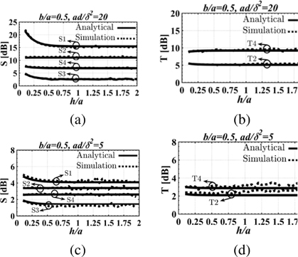
Figure 6: Shielding factor “S” at (a) , (c) and shielding efficiency “T” at (b) and (d) for different observation points as a function of normalized height .
IV. ELECTRIC FIELD SHIELDING
In general, EM waves propagate from one region to another, where their associated electric and magnetic fields are coupled in time and space as described by Maxwell’s equations. This coupling between and is produced by the magnetic induction in Faraday’s law (), and the displacement current density in Ampere’s law (). In the case where EM waves possess slow time varying fields (low frequency) or small dimensions, quasistatic approximations can be considered such that fields become static [20]. The quasistatic laws are attained by neglecting either electric displacement current ( in magnetoquasistatic (MQS) approximation or the magnetic induction ( ) in electroquasistatic (EQS) approximation. In the case of current source, MQS approximations is applied, where time derivative of electric field vanishes. According to Faraday’s law, the slowly varying magnetic field would induce a relatively weak electric field, which is approximately static in nature and almost independent of frequency. This is clearly observed form the 2D E-field maps that are illustrated in Fig. 7. The electric field at lower and higher frequencies are depicted in Figs. 7 (a) and (b), respectively for strip width . Both electric field maps are nearly identical at the two frequencies, which reveal the accumulation of opposite signs of charge at the strip’s sides. Very weak E-fields exist in the region below the shielding strips, which are mainly confined in the slit between the adjacent strips. A smaller gap (i.e., strip’s width ) yields significant reduction in the E-fields, as seen in Figs. 7 (c) and (d) at both low and high frequencies. As a result, E-field shielding can be attained using this configuration.
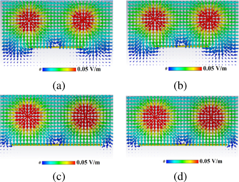
Figure 7: 2D E-field maps for at (a) , (b) , and for at (c) and (d) .
V. CONCLUSION
In this work, an analytical solution of the Laplace equation was presented using Fourier series expansion. This method was used to study the shielding behavior of a system comprising parallel conductive strips separated by small slits. The performance was characterized by evaluating the shielding factor in the region below the shield. Moreover, the performance of the presented shielding system is compared with a continuous conductive sheet, which is manifested by the shielding efficiency. The effect of system parameters was studied in terms of shielding performance. The results have concluded that the proposed system behaves as a full plane when the normalized strip width is at least 0.8. This arrangement of conductive strips with slits adds an extra degree of flexibility compared to a continuous conductive plane shield, which could find some future application in magnetic shielding technology. The analytical results were also confirmed using computer simulation. The performance of the mathematical model was in very good agreement with the numerical simulation.
REFERENCES
[1] S. B. Kim, J. Y. Soh, K. Y. Shin, J. H. Jeong, and S. H. Myung, “Magnetic shielding performance of thin metal sheets near power cables,” IEEE Transactions on Magnetics, vol. 46, no. 2, pp. 682-685, 2010.
[2] O. Bottauscio, M. Chiampi, and A. Manzin, “Numerical analysis of magnetic shielding efficiency of multilayered screens,” IEEE Transactions on Magnetics, vol. 40, no. 2, pp. 726-729, Mar. 2004.
[3] L. Sandrolini, A. Massarini, and U. Reggiani, “Transform method for calculating low-frequency shielding effectiveness of planar linear multilayered shields,” IEEE Transactions on Magnetics, vol. 36, no. 6, pp. 3910-3919, Nov. 2000.
[4] X. Di, “Magnetic shielding using electrical steel panels at extremely low frequencies” (doctoral dissertation, Cardiff University, UK), ProQuest Dissertations and Theses Global, 2008
[5] H. H. Park, J. H. Kwon, S. I. Kwak, and S. Ahn, “Magnetic shielding analysis of a ferrite plate with a periodic metal strip,” IEEE Transactions on Magnetics, vol. 51, no. 8, pp. 1-8, Aug. 2015.
[6] T. Saito and T. Shinnoh, “Applications using open-type magnetic shielding method,” Journal of the Magnetics Society of Japan, vol. 34, no. 3, pp. 422-427, 2010.
[7] Y. Du and J. Burnett, “Magnetic shielding principles of linear cylindrical shield at power-frequency,” Proceedings of Symposium on Electromagnetic Compatibility, pp. 488-493, 1996.
[8] A. M. Dagamseh, Q. M. Al-Zoubi, Q. M. Qananwah, H. M. Jaradat, “Modelling of electromagnetic fields for shielding purposes,” Applied Computation Electromagnetics Society (ACES) Journal, vol. 36, no. 8, pp. 1075-1082, Aug. 2021.
[9] S. K. Burke and T. P. Theodoulidis, “Impedance of a horizontal coil in a borehole: a model for eddy-current bolthole probes,” J. Phys. D: Appl. Phys., vol. 37, no. 3, pp. 485-494, Jan. 2004.
[10] Y. Zhilichev, “Analytical solutions of eddy-current problems in a finite length cylinder,” Advanced Electromagnetics, vol.7, no. 4, pp. 1-11, Aug. 2018.
[11] X. Mao and Y. Lei, ”Analytical solutions to eddy current field excited by a probe coil near a conductive pipe,” NDT & E International, vol. 54, pp. 69-74, Mar. 2013.
[12] V. L. Boaz, “Eddy current losses due to alternating current strips,” IEEE Transactions on Power Apparatus and Systems, vol. 94, no. 1, pp. 1-9, Jan. 1975.
[13] A. Efremov, S. Ventre, L. Udpa, and A. Tamburrino, “Application of Dirichlet-to-Neumann map boundary condition for low-frequency electromagnetic problems,” IEEE Transactions on Magnetics, vol. 56, no. 11, pp. 1-8, Nov. 2020.
[14] Z. Zeng, L. Udpa, S. S. Udpa, and M. S. C. Chan, “Reduced magnetic vector potential formulation in the finite element analysis of eddy current nondestructive testing,” IEEE Transactions on Magnetics, vol. 45, no. 3, pp. 964-967, Mar. 2009.
[15] J. R. Nagel, “Finite-difference simulation of eddy currents in nonmagnetic sheets via electric vector potential,” IEEE Transactions on Magnetics, vol. 55, no. 12, pp. 1-8, Dec. 2019.
[16] J. R. Nagel, “Induced eddy currents in simple conductive geometries: Mathematical formalism describes the excitation of electrical eddy currents in a time-varying magnetic field,” IEEE Antennas and Propagation Magazine, vol. 60, no. 1, pp. 81-88, Feb. 2018.
[17] B. de Halleux, O. Lesage, C. Mertes, and A. Ptchelintsev, “Analytical solutions to the problem of eddy current probes consisting of long parallel conductors,” in D. O. Thompson and D. E. Chimenti, eds, Review of Progress in Quantitative Nondestructive Evaluation, vol. 15, pp. 369-375,1996.
[18] S. Celozzi, R. Araneo, and G. Lovat, Electromagnetic Shielding, Wiley, Hoboken, NJ, USA, 2008.
[19] CST Microwave Studio, ver. 2014, Computer Simulation Technology, Framingham, MA, 2014.
[20] H. A. Haus and J. R. Melcher, Electromagnetic Fields and Energy, Prentice Hall, Englewood Cliffs, NJ, USA, 1989.
BIOGRAPHIES

Hamzeh M. Jaradat received the Ph.D. degree in electrical and computer engineering from the University of Massachusetts Lowell (UML), USA. His current research includes electromagnetics modeling.

Qasem M. Qananwah received the Ph.D. degree in biomedical engineering from Karlsruhe Institute of Technology, Karlsruhe, Germany. His research interest focuses on instrumentation systems, design, and modeling.

Ahmad M. Dagamseh received his Ph.D. degree from the University of Twente in the Netherlands in 2011 in MEMS. His research interests include sensors, instrumentation systems, and modeling.

Qasem M. Al-Zobi received his Ph.D. degree from the Technische Universitaet Berlin, Germany in 1990. His research interests include industrial electronics and external magnetic field screening.
ACES JOURNAL, Vol. 38, No. 8, 625–632
doi: 10.13052/2023.ACES.J.380810
© 2023 River Publishers


