A Sector Ring Shape UWB Antenna by Tightly Coupling
Ziqin Wang, Zhihao Chen, Zhengming Tang, Lam Phav, and Fangyuan Chen
1School of Electronic Information Engineering, China West Normal University
Shida Rd, Nanchong, Sichuan Province, 637000, China
2Jinyichang Science and Technology Co. Ltd
398 Zhenye Rd., Jiaxing, Zhejiang Province, 314000, China
fangyuanscu@gmail.com
3Ministry of Post and Telecommunications of Cambodia
Building 13, Monivong Blvd, Sangkat Srah Chak, Khan Daun Penh, Phnom Penh, 120210, Cambodia
Submitted On: February 7, 2023; Accepted On: June 12, 2023
ABSTRACT
In this paper, a sector ring shape UWB microstrip antenna based on the tight coupling is proposed. The continuous current and electric field distribution are formed by the coupling effect between microstrip patches. This design expanded the bandwidth of this antenna and realized a high-gain performance. To achieve the miniaturization design, the ring microstrip patches are staggered and the ground is removed to effectively reduce the size of the antenna. The ring shaped antenna has a 31 mm outside diameter and a 21 mm inside diameter, with a 2 mm thick substrate.
Besides the excellent mechanical features, such as being compact and easy to fabricate, the proposed antenna also shows good characteristics in radiation patterns and time-domain behaviors. The results show that the antenna achieves the effect of S less than -10 dB in the working frequency band of 2 GHz to 8 GHz, and the simulated results are in good agreement with the measured ones. The antenna realizes low profile and broadband in a novel approach, and this antenna can be used in V2X vehicle systems and IoT networks.
Index Terms: tightly coupling, UWB.
I. INTRODUCTION
The concept of tight coupling was first proposed by Ben Munk in Wheeler’s theory of Continuous Current Sheet Array (CCSA) [1], [2]. The novel interfingered dipoles were applied to the design of the tightly coupled array (TCA) antenna, the elements with coupling capacitors to extend the bandwidth to 4.5:1, which is widely used in antenna design. Volakis et al. used the rectangular spiral structure to realize the tightly coupled antenna with a bandwidth of 10:1; however, it has the disadvantage of complicated antenna unit design [3]. Li introduced a firmly coupled dipole structure with 1/10 wavelength to extend the frequency band [4]. In subsequent studies, it was found that when the distance between the array and the ground was half of the working wavelength, a short circuit effect would be caused, limiting the expansion of impedance bandwidth. Typically, a single or multi-layer dielectric plate is loaded above the array as a wide-angle matching layer, but this increases the profile and quantity of the antennas, which is not conducive to miniaturization design.
Traditional antennas transmit and receive electromagnetic waves through the radiation arm and the ground, the principle of which is to reflect electromagnetic waves through the ground. The general principle is to meet the performance of the antenna, such as gain, impedance matching, direction diagram, etc. As a novel way, the tight coupling can not only achieve effective radiation but also meet the effects of broadband antenna, low profile and high radiation efficiency. In order to avoid the coupling effect between the elements, the space between the elements of the traditional multi-element antenna is usually large. So the antenna size is large, and it is difficult to integrate and conform, greatly limiting the application scenarios of the antenna. In Luo’s study, the size of the antenna reached a radius of 75 mm and a thickness of 3 mm. The antenna only operates in the dual-band Wi-Fi bands 2.37 GHz to 2.63 GHz and 5.52 GHz to 6.37 GHz [5]. Mohsen Gholamrezaei proposed a ring sector slot antenna that can achieve ultra-wideband characteristics of 3.48–5.5 GHz, 5.18–7.35 GHz, and 6.06–8.05 GHz on a floor of 32 35 mm by etching a sector ring groove [6]. Moreover, a low-profile six-port circular patch antenna achieves 3:1 voltage standing wave ratio (VSWR) in the frequency band 5.8-7.5 GHz, with a floor diameter of 45 mm. [7]
However, the antenna profile can be greatly reduced while forming broadband by introducing the tightly coupling effect between antenna elements. Contrary to the traditional antenna, the TCA uses the capacitive coupling effect between the elements to form a continuous current distribution and expand the antenna bandwidth. Therefore, the antenna structure is compact and the antenna size can be effectively reduced. It is more easily integrated into key systems such as automobiles and unmanned aerial vehicles. [8]
In this research, a novel design of a low-profile broadband antenna is presented. Several fan-ring microstrip patches are placed on the upper and lower sides of a ring-shaped dielectric substrate. These two layers of fan-ring microstrip patches are interspersed with each other, and radiation is carried out through the mutual coupling between the microstrip patches. Due to the special nature of the tight coupling, the ground is removed so that a circular cavity can be cut in the middle of the antenna to facilitate the integration of the antenna on different devices. The antenna proposed in this paper can reach the bandwidth of 2 GHz to 8 GHz under the condition that S is less than -10 dB.
In this design, the key parameters that influence the performance of the antenna are studied: the area of overlap between the top and bottom sides of the antenna, the radius of the ring, the spacing between the segments, and the equivalent circuit with inductances and capacitances. The proposed antenna presents advantages such as easy manufacturing and good radiation efficiency characteristics in the operating frequency band.
II. ANTENNA DESIGN AND ANALYSIS
A. UWB antenna design
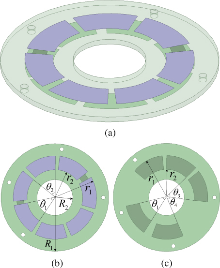
According to the design of the annular antenna, a ring-shaped microstrip structure is placed on a medium substrate, and a ground is placed on the back. The ring microstrip antenna is concentrically divided into seven equal-angle fan rings, and the feeding position is placed between the two fan rings. The ground was further removed by coupling and replaced by five fan ring microstrip patches on the lower layer. In this design, two microstrip patch antennas connected to the feed port form an equivalent dipole antenna. The bandwidth is extended by coupling capacitors in the form of interleaved upper and lower radiation patches. By adjusting the different radius of the sector ring and the number of layers, results can be optimized below -10 dB. In this section, the evolution of the antenna and the optimization process of key parameters are discussed. ANSYS Electronics 2021R is used for the numerical simulation of antennas.
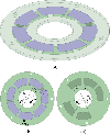
Figure 1 (a) shows the structure of the proposed antenna, and Fig. 1 (b) shows the geometric size of the proposed antenna. Figures 1 (b) and (c) show the dimensional parameters of the upper and lower elements of the antenna, respectively. The dielectric substrate material is FR4 (with 2 mm thickness, = 4.4), with an outer diameter R= 39 mm and an inner diameter R= 13 mm. The thickness of the copper layer on the microstrip patch is 0.018 mm, the outer diameter r of the upper fan ring is 31 mm, the inner diameter r is 21 mm, and the is 51 degrees. Seven concentric copper fan rings patches are printed on the top side of the FR4.
The inner and outer diameters of the five fan rings at the bottom side have the same geometry size as the upper layer. The five fan rings patches of the bottom layer are interspersed with those of the upper layer. The cross-placing layout of upper and lower copper layers is to maximize the coupling effect between the patches. Four asymmetric holes are made for positioning and adhesive fixation. The coaxial feed is selected to ensure the 50 characteristic impedance at the antenna input. Recommended antenna parameters are shown in Figure 1, and the values are listed in Table 1.
Figure 1: Antenna geometry structure: (a) top view, (b) upper layer, and (c) bottom layer.
Table 1: Parameters of the proposed antenna
| Parameter | ||||
| Dimension (mm) | 39 | 13 | 31 | 21 |
| Parameter | ||||
| Dimension | 45 | 51 | 53 | 50 |
Two adjacent microstrip patches on the upper surface form an excitation drive unit; the remaining microstrip patches are used as the coupled radiation parasitic part of the excitation drive unit. The excitation drive unit excites other microstrip patches on the surrounding and bottom surface. The source of the excitation signal is established in the space between two adjacent microstrip patches that constitute the excitation unit. As a result, the high-frequency resonance of the microstrip patch is also constituting the excitation drive unit. The parasitic unit receives the electromagnetic wave generated by the high-frequency resonance of the excitation drive unit through coupling radiation. The microstrip patch that is not directly fed and does not generate the high-frequency resonance is excited by the adjacent patches. When the antenna is working, the excitation drive unit provided with feeding lines can be considered as the network port of the whole antenna.
The overall parameters of the tightly coupled UWB antenna unit are described by the normalized output to input voltage ratio of the antenna. For the radiated electromagnetic wave between the microstrip patches, the incident electromagnetic wave on the corresponding microstrip patch can be expressed as
| (1) |
The normalized reflected electromagnetic wave of the corresponding microstrip patch on the microstrip patch is expressed as
| (2) |
Therefore, the ratio of output and input voltage at the port of the matching network of tightly coupled UWB antennas is expressed as:
| (3) |
The overall S-parameter matrix of the matching network of tightly coupled UWB antennas in the system is shown as follows:
| (4) |
where , , ……, is used to represent the incident wave of N ports, , , ……, is used to represent its reflected wave, and is used to represent that when the incident wave is used to connect the corresponding device port , all ports except the device port are terminated with matching load. Therefore, as long as the reflected wave at the port is measured, the corresponding S-parameters can be measured. To characterize the impedance matching characteristics of microstrip patches of different tightly coupled UWB antennas and the coupling characteristics between different microstrip patches the value range of and is 1 n, where n is the total number of several microstrip patches.
If all ports terminate in reference loads, there will be no reflections. A re-formation of the relationships allows for an observation of how S-parameters define all voltages reflected from any port . The voltage port term is the sum of the incident voltage and the reflected voltage. The coupling effect between the excitation-driven microstrip patch and the parasitic microstrip patch in the tightly coupled UWB antenna unit can be equivalent to the mutual coupling effect between the multiple ports [9]. The corresponding voltage of the port between different microstrip patches is
| (5) |
where is the input impedance of the microstrip patch , is the mutual impedance between the microstrip patch and microstrip patch , is the corresponding port current between different microstrip patches, and is the corresponding port current between different microstrip patches.
As for each microstrip patch of tightly coupled antenna, its performance can be obtained.
The shape, size, and distance of each radiation patch are adjusted to form different degrees of coupling, to achieve inconsistent voltage, current, and peripheral field intensity on the antenna patch.
B. Parameters Analysis
In this design, the coupling effect between the same layer of fan ring microstrip patch units can be regarded as a capacitor, as well as between the microstrip patch units between different layers. Adjusting the distance between them can achieve the effect of adjusting the capacitance value. In order to achieve the desired coupling effect, it is necessary to design and adjust the sweep angle of each fan ring element, the gap between the same layer of fan ring elements, and the interlocking angle between the upper and lower layers.
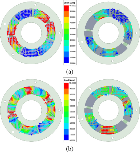
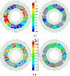
Figure 2: Current distribution of the antenna: (a) 2.45 GHz and (b) 5.5 GHz.
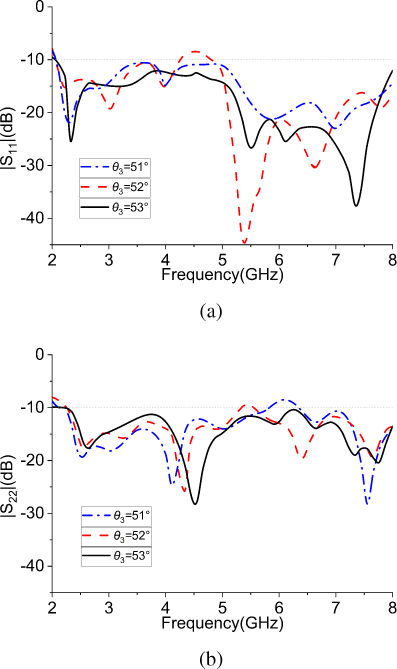
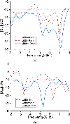
Figure 3: The evolution of the proposed antenna: (a) Sand (b) S.
Figure 2 shows the surface current at 2.45 GHz and 5.5 GHz. As can be seen from Fig. 3, adjusting the spacing between patches shows that the coupling effect between patches has a vital effect on the full frequency band. After optimization, it is concluded that the antenna is well matched at =53, and the whole frequency band is below -10 dB. The difference indicates that the spacing between antenna elements also means that the capacitance formed between antenna elements is not the same, resulting in different coupling effects. Adjusting its spacing can make reasonable use of the coupling effect between antenna elements to achieve good matching and bandwidth widening.
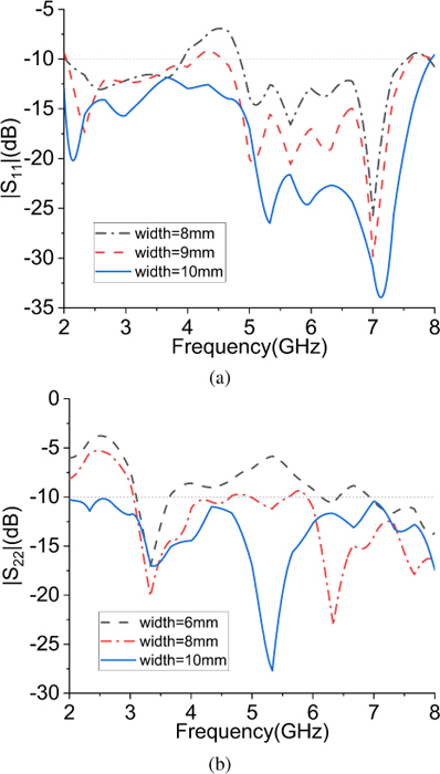
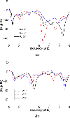
The width is r minus r. As shown in Fig. 4, adjusting the width will affect the matching of the antenna. To achieve the target S and S at the same time, the length with width=10 mm is selected.
Figure 4: The width evolution of the proposed antenna: (a) S and (b) S.
C. Equivalent Circuit
To demonstrate the working principle of the antenna from the point of view of the circuit, the simplified equivalent circuit model is used to analyze the antenna. The Fig. 5 shows the equivalent circuit model of the fan-ring-shaped antenna. It can be seen that a fan-ring microstrip patch can be considered as a set of inductors, capacitors and resistors in parallel. Therefore, the feed radiation patch is represented by L, C, R and the parasitic coupling patch is represented by L, C, R.
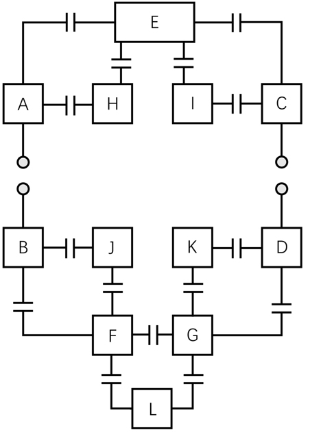
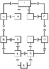
The equivalent circuit of a fan ring microstrip patch antenna is simplified into a module. The equivalent circuit of the antenna is presented as shown in Fig. 6, where A, B, C, D, E, F and G are the upper metal microstrip patch, and H, I, J, K and L are the metal microstrip patch staggered between the lower layer and the upper patch. In this analysis, the strongly coupled antenna element is taken into consideration. The coupling between the patches is represented by a capacitor. According to the above analysis, to change , which means change the capacitance between the two modules, has a great impact on the coupling effect.
Figure 5: Two loop antennas couple equivalent circuits.
Figure 6: Antenna equivalent circuit.
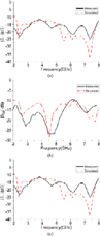
Figure 7: Simulated and measured S-parameters of the proposed antenna: (a) S, (b) S, and (c)S.
III. RESULTS AND ANALYSIS
The antenna was manufactured and measured according to the design concepts and dimensions indicated above. As shown in Fig. 7, the scattering parameter S and S of the antenna was measured using the R&S ZNB40 vector network analyzer (the solid line), versus to the simulated results (the dashed line). The simulated curve and tested curved match well. It can be seen that both (a) S and (b) S are below -10 dB and the isolation degree (c) S is below -20 dB. The whole antenna has reached the ideal standard. The fabricated prototype shows a wide operating band as indicated in the simulation study.
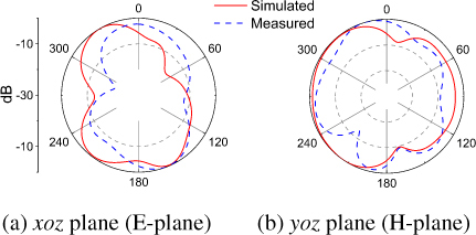
Figure 8 (a) and 8 (b) show the simulated and measured far-field radiation patterns in the xoz plane(E plane) and yoz plane (H plane) at a frequency of 5.5 GHz, respectively. Figure 8 shows that this antenna has a good omnidirectional radiation pattern in the E-plane and in the H-plane. In the E plane, the simulated and measured patterns are less consistent, this is due to the deformation of the 3-D pattern in the xoz plane.
Figure 8: The radiation patterns of (a) E-plane and (b) H-plane at 5.5 GHz.
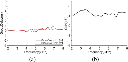
To verify the time-domain performance of the proposed antenna, the group delay is also measured. In Fig. 9 (a), the measurements were made by placing two antennas facing each other at a distance of 30 cm.
Figure 9: (a) Measured group delay and (b) measured peak gains.
The antenna gain is greater than 4 dBi within the entire working frequency band, which shows good radiation performance as an omnidirectional antenna. The maximum gain of this antenna reaches 7.05 dBi at 3.5 GHz
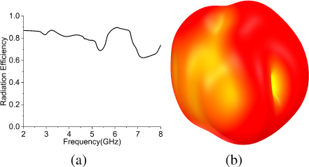
Figure 10 shows the radiation efficiency and 3D pattern of this antenna. The average radiation efficiency reaches 79.5% from 2 GHz to 8 GHz, as tested in the anechoic chamber. The efficiency fluctuates as the frequency changes. This is due to the variation of the current distribution at different working frequencies. The current distribution led to a non-uniform electromagnetic field coupling effect. As can be seen from Fig. 10 (a), the working efficiency is higher at the starting working frequency at 2 GHz. The radiation efficiency decreases when the frequency increases. This is because the EM wave coupling effect is strong at low frequencies, and the effects are less strong when the wavelength is shortened in a higher frequency range.
Figure 10: (a) The radiation efficiency and (b) the 3D Pattern in 5 GHz.
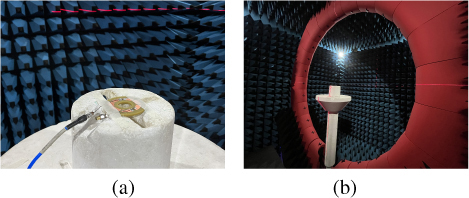
Figure 11: The antenna in anechoic chamber.
Table 2: Performance comparison with other works
| Reference Work | Bandwidth (GHz) | Gain (dBi) | Size(mm) | Efficiency |
| [5] | 2.37-2.635.52-6.37 | 6 | Ø75 | / |
| [6] | 3.48-5.55.18-7.35 | 4.25 | 3235 | 90% |
| [7] | 5.8-7.5 | / | Ø45 | 63% |
| [8] | 1.5-4.5 | 11.8 | 104104 | / |
| [10] | 2.24-2.535.42-5.98 | 7.5 | Ø170 | 80% |
| Proposed work | 2-8 | 7.05 | Ø78(outside)Ø26(inside) | 79.5% |
IV. CONCLUSION
In this research, a low-profile wideband antenna tight coupling radiation is proposed. By placing the etched radiation patch on the upper and lower layers, a 2GHz to 8GHz radiation band is achieved. The ground structure is eliminated and the antenna miniaturization is realized. The equivalent circuit is provided and discussed, and the key parameters are studied. Then, the prototype of the proposed antenna is manufactured and its performance is tested. S simulated and measured. Radiation mode, group delay, and maximum gain were compared, showing good agreement. All these good properties make the proposed tightly coupling low-profile broadband antenna a good candidate for the communication system.
ACKNOWLEDGMENT
This work is supported by the Nanchong Key Laboratory of Electromagnetic Technology and Engineering. Jinyichang Science and Technology Co., Ltd. provides hardware support, technical assistance, and the test environment.
REFERENCES
[1] B. A. Munk, Finite Antenna Arrays and FSS, John Wiley & Sons, New York, 2007.
[2] H. Wheeler, “Simple relations derived from a phased-array antenna made of an infinite current sheet,” IEEE Transactions on Antennas and Propagation, vol. 13, no. 4, pp. 506-514, July 1965.
[3] E. A. Alwan, K. Sertel, and J. L. Volakis. “A simple equivalent circuit model for ultrawideband coupled arrays,” IEEE Transactions on Antennas and Propagation, vol. 60, no. 11, pp. 117-120, Jan. 2012.
[4] W. Li, S. Gao, L. Zhang, Q. Luo, and Y. Cai. “An ultra-wide-band tightly coupled dipole reflectarray antenna,” IEEE Transactions on Antennas and Propagation, vol. 66, no. 2, pp. 553-540, Dec. 2017.
[5] Luo, Z. Kai, T. Su, and K. D. Xu. “A single-layer low-profile dual-wideband monopolar patch antenna with shorting vias and parasitic annular sectors,” IEEE Antennas and Wireless Propagation Letters, Oct. 2022.
[6] M. Gholamrezaei, F. Geran, and R. A. Sadeghzadeh, “Completely in-dependent multi-ultrawideband and multi-dual-band frequency reconfigurable annular sector slot antenna (FR-ASSA),” IEEE Transactions on Antennas and Propagation, vol. 65, no. 2, pp. 893-898, Nov. 2016.
[7] K. L. Wong, C. J. Ho, and W. Y. Li, “Low-profile six-port circular patch antenna with six triple-shorted dual-resonant 60-disk sectors to generate six uncorrelated waves for wideband mobile MIMO antennas,” IEEE Access, pp. 80277-80288, Aug. 2022.
[8] Y. Fu, Y. Zhang, Q. Shi, M. Temiz, A. El-Makadema, and J. Shi, “A foldable tightly coupled crossed rings antenna array of ultrawide bandwidth and dual polarization,” IEEE Access, pp. 86684-86695, Aug. 2022.
[9] T. R. Vogler, “Analysis of the radiation mechanisms in and design of tightly-coupled antenna arrays,” Diss. Virginia Tech, 2010.
[10] S. Gao, L. Ge, D. Zhang, and W. Qin, “Low-profile dual-band stacked microstrip monopolar patch antenna for WLAN and car-to-car communications,” IEEE Access, pp. 69575-695816, Oct. 2018.
[11] Z. F. Wu, W. J. Lu, J. Yu, and L. Zhu, “Wideband null frequency scanning circular sector patch antenna under triple resonance,” IEEE Transactions on Antennas and Propagation vol. 66, no. 11, pp. 7266-7274, May 2020.
[12] S. M. Moghaddam, J. Yang, and A. U. Zaman, “Fully-planar ultrawideband tightly-coupled array (FPU-TCA) with integrated feed for wide-scanning millimeter-wave applications,” IEEE Transactions on Antennas and Propagation, vol. 68, no. 9, pp. 6591-6601, June 2020.
[13] B. Wang, S. Yang, Y. Chen, S. Qu, and J. Hu, “Low cross-polarization ultrawideband tightly coupled balanced antipodal dipole array,” IEEE Transactions on Antennas and Propagation, vol. 68, no. 6, pp. 4479-4488, Feb. 2020.
[14] H. Zhang, S. Yang, S. Xiao, Y. Chen, and S. Qu, “Low-profile, lightweight, ultra-wideband tightly coupled dipole arrays loaded with split rings,” IEEE Transactions on Antennas and Propagation, vol. 67, no. 6, pp. 4257-4262, Mar. 2019.
BIOGRAPHIES

Ziqin Wang received the B.E. degree in applied electronic engineering from China West Normal University, Nanchong, China, in 2020. He is currently pursuing the master’s degree in electronic information engineering at China West Normal University, Nanchong, China. He was an intern at the Jinyichang Science & Technology from 2022 to 2023. His research interests include microwave theory, numerical computation in electromagnetics, and antenna design.

Zhihao Chen received the B.E. degree in communication engineering from China Jiliang University, HangZhou, China, in 2021. He is currently pursuing the master’s degree in electronic information engineering at China West Normal University, Nanchong, China. He was a teaching assistant at the school of electronic information engineering of China West Normal University. His research interests include microwave theory and technology, and antenna design.

Zhengming Tang received his M.S. degree in electrical engineering from Southwest Jiaotong University in 2012, and his Ph.D. degree from Sichuan University in 2016. Now he is a professor in the School of Electronics and Information Engineering, China West Normal University, Sichuan, China. His research interests are microwave heating, microwave theory, and microwave chemistry.

Fangyuan Chen received his Ph.D. degree in radio physics at Sichuan University, Chengdu, China, in 2016. From 2013 to 2015 he was a visiting doctoral student at Cornell University, New York, USA. Now he is the deputy chief engineer of Jinyichang Science & Technology Co., Ltd. Currently, he is responsible for strategic technology development in V2X network architecture design, multi-band frequency antenna design. His research interests are microwave theory and technology, and optimization algorithms.

Lam Phav received his B.E degree in computer science and engineering, from Royal University of Phnom Penh, Cambodia, in 2004. He received the M.Sc. degree in communication information systems, from Sichuan University, Chengdu, Sichuan, China, in 2013. Currently he is working at the General Department of Information and Communication Technology, Ministry of Post and Telecommunications (MPTC), Phnom Penh, Cambodia. His research intetrests are antenna theory and design, wireless communication technology.
ACES JOURNAL, Vol. 38, No. 9, 717–724
doi: 10.13052/2023.ACES.J.380912
© 2023 River Publishers
