A Compact Bandpass Filter with Active Switchable Passband Status
Ruofeng Xu, Wei Tang, Jun Wang, and Lei Zhao*
1School of Information and Control Engineering
China University of Mining and Technology, Xuzhou, 221116, China
xuruofeng@cumt.edu.cn, 383028707@qq.com, jun-wang@cumt.edu.cn, leizhao@cumt.edu.cn*
Submitted On: March 2, 2023; Accepted On: October 27, 2023
ABSTRACT
In order to meet the increasing demand for adjustable devices in the modern wireless communication system, a compact bandpass filter with active switchable passband is proposed. The filter is based on the half mode substrate integrated waveguide (HMSIW), and uses its cut-off characteristics to form the lower stopband. The resonant characteristics of a quarter-wavelength shorted stub generates a transmission zero (TZ) at higher frequency, which forms the upper stopband. The active control of DC power supply determines the biased states of PIN diodes to change the electrical size of the filtering parts. When the diodes are reverse biased, the filter works in C band with the passband of 3.9-5.2 GHz; when the diodes are forward biased, the passband shifts to S band of 2.7-3.6 GHz. The 28.6% relative bandwidth in both frequency bands remains constant. The simple design realizes the active switching between bands, providing a promising idea for active adjustable devices.
Index Terms: Active, bandpass filter, half mode substrate integrated waveguide, switchable.
I. INTRODUCTION
The bandpass filter is one of the most important parts in satellite radar communication systems, microwave communication systems, wireless transceiver systems, and other electromagnetic devices, which can effectively ensure the signal transmission in the target frequency band and shield against interference. While traditional filters can provide excellent bandpass performance in the fixed frequency band with advantages of simple structures and steady characteristics, they lack the ability of the multiband selection and adjustment. As the growing demand of high-integration and reconfigurable devices in wireless communication systems, the technical need rises rapidly for compact active tunable filters with multifunctional features, like wideband tuning, easy implementation, low cost, etc. To meet these requirements, DC controlled units are integrated into the structure to dynamically change the distribution characteristics of the electromagnetic field during propagation, which can enable a single filter to efficiently process multiple signals in different frequency bands [1–3].
Currently, most tuning studies mainly focus on microstrip filters. By utilizing the on/off characteristics of the classic PIN diode, the planar microstrip lines can be easily accessed or disconnected from the filtering part, which changes the resonant size. Thus, adjustment of the center frequency, working frequency, or bandwidth can be achieved. A reconfigurable bandpass filter was introduced that can generate passbands in multiple frequency bands by controlling different combinations of the microstrip stubs [4]. A switchable filter was constructed by a set of microstrip lines. The switch between the ultra-wideband and wideband was determined by the connection of high impedance quarter-wavelength shorted stubs or a shorted stepped impedance resonator [5]. A reconfigurable dual-band bandpass filter was designed, which can alter three bandwidths through the control of PIN diodes without changing the center frequency [6]. However, due to the multiple harmonic effect of the microstrip line, it is difficult to achieve high isolation and broadband regulation. Moreover, the active feed network is relatively complex. Therefore, the studies turn to the active tuning of the substrate integrated waveguide (SIW) filter.
The SIW structure has the advantages of low loss, easy integration, and low cost [7]. The PIN diode works as a microwave switch to shift between different components in the guide-wave structure. The electrical control unit changes the combination or the values of the distributed impedances in the cavity to alter the propagation characteristics [8, 9]. An adjustable SIW filter was demonstrated by using the PIN diode to connect the different lengths of slot lines in the cavity. The center frequency can be changed with a 30 MHz bandwidth expansion [10]. But the overlap of each passband was a bit high, and the introduction of additional parasitic elements led to the narrow adjustable band and bandwidth. A switchable SIW filter realized the band and bandwidth switching among three center frequencies through the connections of corresponding metal vias in different positions of the cavity [11]. However, the links and bias networks for inner vias increased the processing complexity, and the parasitic inductance brought additional insertion loss. Due to the high integration of the SIW structure and the limitation of available parameter adjustment, there is little research on the filter of the wide-range and cross-band active switch by using PIN diodes.
This paper presents a compact switchable half mode substrate integrated waveguide (HMSIW) filter, which realizes the bandpass feature through the coupling between the fundamental mode of HMSIW and the resonance of a quarter-wavelength shorted stub. The active switching changes the electrical size of the filtering part by utilizing the on/off status of PIN diodes in order to switch the passband between the S band and C band with constant relative bandwidth. When the diodes are reverse biased, the passband is from 3.9 GHz to 5.2 GHz in the C band, centers at 4.55 GHz with a relative bandwidth of 28.6%. When the diodes are forward biased, the passband shifts to 2.7-3.6 GHz in the S-band, centers at 3.15 GHz, without changing the relative bandwidth. The measured and simulated results show good agreement and validate the feasibility of this technology for achieving cross-band switching in SIW filters.
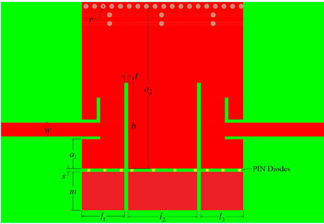
Figure 1: Top view of the filter.
II. FILTER DESIGN
A. Structures
The structure of the proposed bandpass filter is shown in Fig. 1, and the relative parameters are listed in Table 1. The structure consists of an upper metal layer, a middle dielectric layer, and a bottom ground plane. The feedline section adopts the microstrip line to coplanar waveguide (CPW) construction and introduces transverse slots at the terminal of the CPW to further reduce port reflections. The functions of the bandpass filtering and band switching are primarily accomplished by altering the configuration of the upper metal layer. The open side of the middle substrate acts as an equivalent magnetic wall of HMSIW. A line of metal vias spaced much less than quarter-wavelength act as an equivalent electric wall on the other sidewall of the substrate; an extra six metal vias are horizontally oriented very near to the electric wall to enhance out-of-band suppression. Two surface slots are arranged at a distance from the side of the metal vias and connected longitudinally on the upper metal layer, creating a quarter-wavelength shorted stub. This part constitutes the filtering structure in the C band.
Table 1: Parameters of the structure
| Symbol | |||||
|---|---|---|---|---|---|
| 2.75 | 14.9 | 3.97 | 6.44 | 3.97 | |
| Symbol | |||||
| 7.95 | 0.3 | 0.3 | 3.6 | 1.28 |
Three rectangular metal pads with the same width are placed longitudinally at a very short distance from the open end of the HMSIW. The gaps between the metal sheets correspond to the slots of the shorted stub. These three metal pads are connected to the upper metal layer of the C-band structure via several MADP-000907-14020X PIN diodes, and their welding polarities keep the same directions. The filtering performance will have significant interference by the number of diodes if the two ends of pads are shorted. Therefore, the number of diodes and their spacing have been optimized to ensure minimum parasitic effects to the propagation and surface current. This part constitutes the switching structure of the S band. The DC power supply drives the PIN diodes through ferrite chokes, which can effectively filter high-frequency signals with minimal interference to DC signals. The forward or reverse biased states of the PIN diodes determine whether the switching parts are connected to the filtering structure. The Rogers RT/Duroid 5880 substrate has dielectric thickness of mm, copper foil thickness of 0.035 mm, , and is used as the middle dielectric layer.
B. Active switch realization
The bandpass performance is mainly realized by lower and upper stopbands. The lower stopband is created by the high-pass characteristics of the HMSIW fundamental mode, and the upper stopband is created by the resonance of the quarter-wavelength shorted stub, which generates a transmission zero (TZ) at higher-frequency [12]. The cutoff frequency of HMSIW TE mode and the resonance frequency of the shorted stub are
| (1) |
Here is the speed of light in vacuum, is the relative dielectric constant of the medium substrate, is the equivalent width of HMSIW, and is the waveguide wavelength of the shorted stub in the substrate.
When the PIN diodes are reverse biased, the equivalent width of the waveguide is 14.6 mm, and the cut-off frequency is 3.5 GHz; the length of the shorted stub is 7.9 mm, and the resonant frequency is 7.3 GHz, where the upper TZ appears. Considering a few transition bandwidths, the filter is under the C-band bandpass working status.
When the PIN diodes are forward biased, three metal sheets are connected to the HMSIW structure to change the electrical size, internal impedance distribution, and the resonance characteristics of the filter. Therefore, the equivalent width of the waveguide () increases to 18.5 mm, and the cut-off frequency moves to 2.7 GHz; the length of the shorted stub () increases to 11.7 mm, and the upper TZ is generated at 5 GHz. The actual passband shifts to the S band. Three activated metal sheets enhance the transverse electrical lengths of the waveguide and the shorted stub simultaneously. It leads to a reduction of and respectively, which switches the bandpass to S band. By controlling the states of PIN diodes through the DC circuits, the working status of the bandpass filter can be effectively switched between S and C bands.
The transverse E field of HMSIW TE mode can be expressed as [13]
| (2) |
Here, A is the random amplitude of the wave and is the permeability of the dielectric. As is changed by the bias of diodes, the maximum area of E-field will shift in the TE mode. When the filter works at S band, the extra capacitance created by the air gap is paralleled with the inductance of diodes, which could generate harmonic resonances in the passband. The behavior of the E field can be analyzed by using FEMmethods.
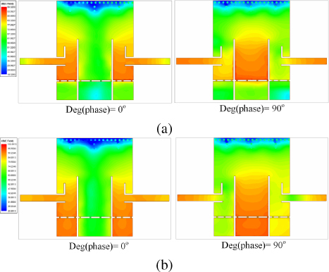
Figure 2 shows the comparison of the electric field distributions at different phases (0 and 90) while working in C band and S band. The PIN diodes are off at C band; thus, the surface electric field propagates as the TE mode of HMSIW, which allows the electromagnetic wave transmitting through the quarter-wavelength shorted stub to produce a bandpass effect. There is little energy coupling to three metal sheets, which have very weak impacts on the performance. When the PIN diodes are activated, the surface current spreads to the metal sheets through the short circuits. Obviously, the electromagnetic distribution still follows the rule of the fundamental mode of HMSIW, but the altering structures of the waveguide and shorted stub form a new bandpass filtering in a lower frequency band. Although the excited position of the feedline is moved to the middle of the waveguide when diodes are active, the fundamental field distributions have very little affection.
Figure 2: Distributions of the electric field at different phases: (a) Propagation in C band and (b) propagation in S band.
III. SIMULATION AND TESTING
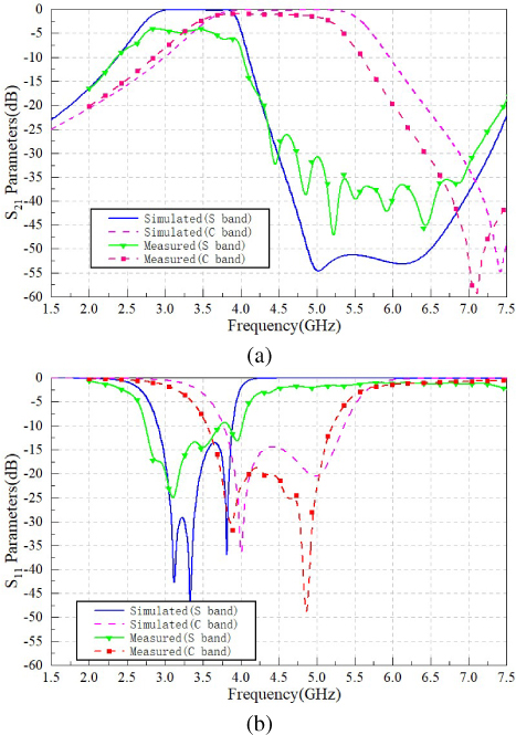
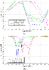
The filter’s structure was simulated using the high frequency structure simulator (HFSS), and the comparison of the simulated and measured results are shown in Fig. 3. The simulated results show that excellent bandpass filtering is achieved in the 4-5.4 GHz band when PIN diodes are reverse biased. The in-band insertion loss is less than 0.3 dB, and the return loss is lower than -15 dB. The upper TZ appears at 7.3 GHz, which greatly improves the selectivity. When the PIN diodes are forward biased, the passband of the filter is switched to the 2.9-3.9 GHz band. The in-band insertion loss is less than 0.5 dB, and the return loss is lower than -13 dB. The upper TZ is moved to 5 GHz, and the out-of-band roll-off is very steep. The relative bandwidth of each status is about 29%, and the simulated results are consistent with the theoretical analysis.
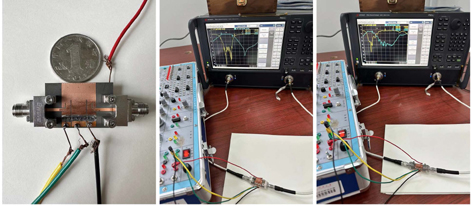
The filter was fabricated by using traditional single-layer print circuit board (PCB) processing technology. Two SMA-KFD0851 connectors work as input/output ports to connect the E5063A network vector analyzer for full-wave simulation testing. The solderless connectors eliminate additional welding losses with only 0.2 dB in-band loss. The fabricated product is shown in Fig. 4 (a). To reduce the ferrite choke’s influence on the top metal layer, this choke was welded on the bottom ground plane, which links the positive pole of the DC power supply. Each metal sheet was welded to one ferrite choke which links the negative pole. Figures 4 (b) and (c) show the testing environment and two working statuses of the filter when switching the biases.
Figure 3: Comparisons between simulated and measured results: (a) Sparameters and (b) S parameters.
Figure 4: Fabricated filter and test environment: (a) Product, (b) passband in C band, and (c) passband in S band.
The measured results in Fig. 3 show that the filter has a passband in C band from 3.9GHz to 5.2GHz when PIN diodes are off. The in-band insertion loss is less than 1 dB and return loss is lower than -18dB. When PIN diodes are forward biased, the passband is switched to S band of 2.7-3.6 GHz, with an insertion loss less than 5 dB and a return loss lower than -10 dB. The relative bandwidth of these two passbands is 28.6%. The active network has a 2-3 ns switching speed. However, the parasitic inductance made two passbands shift to the lower frequency at about 0.3 GHz. Although the in-band insertion loss is relatively larger than simulated ones, the return loss keeps the good performance. It means the additional measured losses are mainly caused by the energy storage elements in the feeding network. More diodes may reduce the in-band loss because better impedance matching will be achieved. Moreover, the welding process increases the surface roughness and brings more losses. These drawbacks can be improved by optimizing the processing technology and isolating circuits. It illustrates that the designed filter can achieve real-time bandpass switching between S and C bands under active control, The passband response and overall trends in the measurement match well with simulated results.
IV. CONCLUSION
This paper presents a HMSIW bandpass filter capable of switching passbands. Detailed theoretical analysis, simulations, and the testing are accomplished. The measured passband can be switched between S band (2.7-3.6 GHz) and C band (3.9-5.2 GHz) under the active control while maintaining a constant relative bandwidth of 28.6%. The designed filter has the advantages of simple structure, low cost, easy realization, and compact size, which is potentially applicable to the reconfigurable filtering devices in microwave communication systems.
REFERENCES
[1] J. S. Hong, “Reconfigurable planar filters,” IEEE Microw. Mag., vol. 10, no. 6, pp. 73-83, Oct. 2009.
[2] C. Lugo and J. Papapolymerou, “Six-state reconfigurable filter structure for antenna based systems,” IEEE Trans. Antennas Propag., vol. 54, no. 2, pp. 479-483, Feb. 2006.
[3] I. Hashinur, D. Saumya, B. Tanushree, and A. Tanweer, “Diode based reconfigurable microwave filters for cognitive radio applications: A review,” IEEE Access, vol. 8, pp. 185429-185444, Oct. 2020.
[4] S. Ramkumar and R. Boopathi, “Compact reconfigurable bandpass filter using quarter wavelength stubs for ultra-wideband applications,” International Journal of Electronics and Communications, vol. 151, 2022.
[5] A. Bandyopadhyay, P. Sarkar, and R. Ghatak, “A bandwidth reconfigurable bandpass filter for ultrawideband and wideband applications,” IEEE Transactions on Circuits and Systems-II: Express Briefs, vol. 69, no. 6, June 2022.
[6] X. K. Bi, X. Zhang, S. W. Wong, S. H. Guo, and T. Yuan, “Reconfigurable-bandwidth DWB BPF with fixed operation frequency and controllable stopband,” IEEE Transactions on Circuits and Systems—II: Express Briefs, vol. 68, no. 1, Jan. 2021.
[7] X. P. Chen and K. Wu, “Substrate integrated waveguide filters: design techniques and structure innovations,” IEEE Microwave Magazine, vol. 15, no. 6, pp. 121-133, 2014.
[8] R. F. Xu, B. S. Izquierdo, and P. R. Young “Switchable substrate integrated waveguide,” IEEE Microwave and Wireless Communication Components Letters, vol. 21, no. 4, pp. 194-196, 2011.
[9] H. D. Chen, W. Q. Che, T. Y. Zhang, Y. Cao, and W. J. Feng, “HMSIW-based switchable units using super compact loaded shunt stubs and its applications on SIW/HMSIW switches,” International Journal of Electronics, vol. 105, no. 6, pp. 1036-1050, 2018.
[10] F. Cheng, P. Lu, and K. Huang, “Center frequency and bandwidth switchable substrate integrated waveguide filters,” International Journal of Microwave and Wireless Technologies, vol. 12, no. 4, pp. 282-287, 2020.
[11] Y. Yi and Y. R. Zhang, “A bandpass filter with switchable frequency and bandwidth on substrate integrated waveguide,” 2021 International Conference on Microwave and Millimeter Wave Technology (ICMMT), pp. 23-26, May 2021.
[12] Y. Q. Wang, W. Hong, Y. D. Dong, B. Liu, H. J. Tang, J. X. Chen, X. X. Yin, and K. Wu, “Half mode substrate integrated waveguide (HMSIW) bandpass filter,” IEEE Microwave and Wireless Communication Components Letters, vol. 17, no. 4, Apr. 2007.
[13] David M. Pozar, Microwave Engineering, Fourth Edition. Beijing: Publishing House of Electronics Industry, 2019.
BIOGRAPHIES

Ruofeng XU received the B.Sc. (2004) degree from Suzhou University in electronics and science and technology and the M.Sc. (2006) and Ph.D. (2010) degrees in electronic engineering from the University of Kent, UK. He had been the visiting scholar (2018) for one year in Rutgers University, USA. Now he has been a lecturer in School of Information and Control Engineering, China University of Mining and Technology. His main research directions are microwave technology and application.

Wei Tang has been a master student at the School of Information and Control Engineering, China University of Mining and Technology. His main researches are on SIW filters and active adjustable filters.

Jun Wang has been a lecturer in School of Information and Control Engineering, China University of Mining and Technology. His main researches are on radio frequency/microwave devices, antennas and transmission, and SPP components.

Lei Zhao has been a professor and doctoral supervisor in School of Information and Control Engineering, China University of Mining and Technology. He has been a senior member of IEEE, member of the Antenna Branch of the China Electronics Society, and chairman of IEEE AP-S Chapter Xuzhou. His main researches are on RF microwave devices, new electromagnetic materials, vortex wave communication, and computational electromagnetics.
ACES JOURNAL, Vol. 38, No. 9, 746–750
doi: 10.13052/2023.ACES.J.380916
© 2023 River Publishers
