High-order Mode of Spoof Surface Plasmon Polaritons based on a Novel Compact Structure and its Application in Band-pass Filters
Siyu Yang, Shuang Liu, Huali Zhu, Fachun He, Dan Lei, Jun Yan, and Chan Gao
1School of Mathematics and Science
Chengdu University of Technology, Chengdu 610000, China
894518884@qq.com, ranranshuangshuang@163.com, 1937604847@qq.com, leidan1008@163.com, gaochan@cdut.edu.cn
2School of Electronic Science and Engineering
University of Electronic Science and Technology of China, Chengdu 610000, China
350342101@qq.com
3China Electronics Technology Group Corporation
10th Research Institute, Chengdu 610000, China
niko_robin@163.com
Submitted On: March 8, 2023; Accepted On: June 5, 2024
ABSTRACT
In this paper, two band-pass filters based on the high-order mode of spoof surface plasmon polaritons (SSPPs) are introduced. A novel compact bow-folded strip is proposed as a cell, which exhibits perfect band-pass characteristics. By adjusting the width and groove of the bow-folded strips, high-order mode can be obtained to support the design of band-pass filters. Compared to the conventional single-side rectangular groove SSPPs cell, our proposed bow-folded strip structure cells reduce the electrical size by 59% and 70% at the same cut-off frequency. In addition, the transmission lines of the two proposed band-pass filters are microstrip lines and their over-conversion structures are simple trapezoidal over. A single-band and a dual-band band-pass filters using the proposed SSPPs cell are fabricated and measured, both having almost the same size. The measured results are in good agreement with simulated results, which verify the feasibility of our design.
Index Terms: band-pass filter, bow-folded strip, novel compact, SSPPs.
I. INTRODUCTION
Surface plasmon polaritons (SPPs) refer to electromagnetic waves that are excited along the surface of metallic media and propagate within the optical frequency range, which have field-bound and field-enhanced properties in the subwavelength range [1]. Due to their strong optical confinement in the subwavelength region and their ability to break the diffraction limit, SPPs have garnered growing attention due to their potential applications in the design of integrated optical components and circuits with high density. In 2004, Pendry and his colleagues proposed the concept of spoof surface plasmon polaritons (SSPPs). SSPPs and SPPs have similar features [2]. The dispersion characteristics of the spoof surface plasmon polaritons can be controlled by directly changing the structure size of the SSPPs cell [3]. As a result, SSPPs research has received a lot of coverage in the microwave and terahertz bands.
However, previously proposed devices based on SSPPs are large-sized bulk structures, which poses a challenge for the integration of SSPPs with microwave and terahertz planar circuits. To solve this problem, Cui and his coworkers proposed the conformal surface plasmons (CSPs) waveguide based on an ultra-thin and flexible film printing grooved metal strip [4, 5], which accelerated the development of SSPPs technology. Since then, different shapes of SSPPs transmission lines have been reported, such as folded [6] and double-sided serrated [7]. Based on this, functional devices based on SSPPs transmission lines, such as filters [8–14], antennas [15–17], power dividers [18–20], frequency dividers [21], and so on, have been extensively investigated.
However, most of the above work is done based on the design of the fundamental mode of SSPPs, which requires complex transmission transitions in the design of transmission lines. For the high-order mode of SSPPs, there is no need to use the complex transmission, only simple microstrip lines are needed to excite effectively. When the groove depth in the SSPPs cell structure is greater than the period, the designed transmission line can operate in the high-order mode state [22]. Some band-pass filters based on the high-order mode of SSPPs have been reported [23–27]. However, these SSPPs structures cannot achieve better size advantages. The transitions of the SSPPs transmission lines are very complex in the instance of multi-frequency filters now being developed [28, 29]. Therefore, it is valuable to study the application of a compact multi-frequency filter based on the high-order mode of SSPPs and a simple SSPPs transmission line.
In this paper, we propose a novel bow-folded strip SSPPs structure based on high-order mode for single-band and dual-band band-pass filters. We study the conventional rectangular groove SSPPs cell and the bow-folded strip SSPPs structure. It is demonstrated that the bow-folded strip SSPPs structure outperforms the traditional SSPPs structure in terms of size and better field binding. The structural characteristics of the SSPPs cell with a bow-folded strip are then examined. The first-order high-order mode of the SSPPs structure is used to construct a single-band band-pass filter by designing the structural parameters. A dual-band band-pass filter is constructed by using the first high-order mode and the second high-order mode using a similar theoretical method. Hence, it indicates the structure’s suitability for designing band-pass filters and the commendable performance of said filters. Moreover, the structure has the advantage of miniaturization.
II. STUDY OF HIGH-ORDER MODE OF SSPPs
In this section, we initially investigate the fundamental mode (Mode 0) and the first high-order mode (Mode 1) of the bow-folded strip SSPPs structure. Subsequently, by employing a straightforward trapezoidal transition, we can successfully excite the Mode 1 of the SSPPs, resulting in the generation of a passband that exhibits exceptional transmission capability.
The SSPPs unit structure based on the bow-folded strip structure is shown in Fig. 1 (b). Unlike the conventional single-side rectangular groove SSPPs unit structure (Fig. 1 (a)), it is formed by etching bow-folded strip on top of the rectangular groove SSPPs unit structure, based on Rogers RT5880 substrate with thickness of 0.508 mm, relative dielectric constant of 2.2 and tangent loss of 0.0009. In order to improve the SSPPs field confinement capability, the backside of the substrate is a continuous metal ground structure [30]. The dimensions of two-unit structures are listed in Table 1. The period is d, the deep grooves are h (slot depth of conventional rectangular groove) and h(slot depth of bow-folded strip), the top edge is length l, and the line widths are W and w, respectively.
Figure 1: (a) Conventional rectangular groove SSPPs cell structure, (b) bow-folded strip SSPPs cell structure, (c) dispersion characteristics of conventional rectangular groove and bow-folded strip SSPPs cells with h=h=6.2 mm, and (d) dispersion characteristics of conventional rectangular groove and bow-folded strip SSPPs cells with h=6.2 mm, h=15 mm.
As stated in the study conducted by [27], the single grating structure of SSPPs demonstrates the ability to sustain high-order modes of SSPPs if the depth of groove h exceeds the period d. The number of SSPPs modes (N) can be denoted by:
| (1) |
Table 1: The dimensions of two-unit structures (unit=mm)
| l | d | h | h | W | w | W | w |
|---|---|---|---|---|---|---|---|
| 4 | 7 | 6.2 | 6.2 | 2 | 2 | 0.5 | 0.5 |
The SSPPs cell structure is simulated using the eigenmode solver of the commercial software CST Microwave Studio. The boundary conditions for the propagating x-direction are specified as periodic boundaries, and the non-periodic y- and z-boundaries are specified as either electric or magnetic boundaries. By setting the intrinsic phase shift between periodic boundary conditions to the parameter phase, one can use the parameter scan function to get the mode frequency. According to the definition, the conversion relation between the intrinsic phase shift value phase and the propagation constant k in the propagation direction is as follows [31]:
| (2) |
According to the dispersion curve in Fig. 1 (c), the dispersion curves of both modes of SSPPs start from the intersection with the dispersion curve of light in free space. As the intrinsic phase shift value increases, it gradually veers away from the light line until reaching the maximum frequency value, known as the cut-off frequency. When the dispersion curves closely approach the cut-off frequency, the field’s binding capability to SSPPs reaches its maximum strength. When h=h=6.2 mm, the cut-off frequency of the conventional rectangular groove cell structure is 7.4 GHz and that of the bow-folded strip cell structure is 3.5 GHz. Therefore, the designed bow-folded strip cell structure in the same size has a lower cut-off frequency than the conventional rectangular groove cell structure, indicating that the transmission line of the bow-folded strip cell structure has a higher field-binding force in the frequency band range of 0 to 14 GHz.
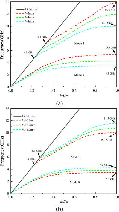
Figure 2: (a) Dispersion characteristics of bow-folded strip SSPPs cells of different l and (b) dispersion characteristics of bow-folded strip SSPPs cells of different h.
Here we investigate the characteristics of the high-order mode, making h=15 mm and h=6.2 mm. At this point the transverse dimension of the designed bow-folded strip structure reduces to 59% of the conventional rectangular groove. The dispersion curves in Fig. 1 (d) show that both the conventional single-side rectangular groove structure and the bow-folded strip appear in high-order mode, and the cut-off frequencies of the fundamental and high-order mode are almost the same for both. The fundamental mode of their cut-off frequency is 3.5 GHz, featuring low-pass characteristics. The first high-order mode cut-off frequency is 10.1 GHz, which exhibits an inherent band-pass. Thus, it is shown that the bow-folded strip structure occupies less area at the same cut-off frequency. The groove depth primarily determines the cut-off frequency of SSPPs, thus leading to this phenomenon. The curved groove of the bow-folded strip SSPPs unitary structure increases the relative effective groove depth of the SSPPs and further reduces the horizontal dimension. In addition, there is no overlap between the fundamental and high-order mode, indicating single-mode propagation for each mode, unlike the conventional rectangular waveguide.
Previous work has shown that the cut-off frequency of SSPPs’ fundamental mode is mainly determined by the groove h. Further, it is also important to investigate the relationship between the high-order mode and the structural parameters of the bow-folded strip SSPPs cell. As shown in Fig. 2 (a), when the width l of the bow-folded strip SSPPs cell is increased from 2 mm to 4 mm, the intersection of the first high-order mode with the light (i.e., the lower cut-off frequency) gradually decreases from 7.1 GHz to 4.8 GHz. The cut-off frequency (i.e., the upper cut-off frequency) gradually decreases from 13.9 GHz to 10.1 GHz. As shown in Fig. 2 (b), when the length h of the bow-folded strip SSPPs cell is increased from 4.2 mm to 6.2 mm, the intersection of the first high-order mode with the light (i.e., the lower cut-off frequency) gradually decreases from 6.1 GHz to 4.8 GHz, and the cut-off frequency (i.e., the upper cut-off frequency) gradually decreases from 11.5 GHz to 10.1 GHz. As a result, the structural characteristics of the bow-folded strip can influence the passband frequency range created by the first-order higher mode, and the desired passband can be flexibly altered by choosing alternative structure sizes. As can be seen in Fig. 2, the groove depth h and width l affect the cut-off frequency of the high-order mode, so the desired passband can be flexibly adjusted by setting different structural dimensions.
III. IMPLEMENTATION OF BAND-PASS FILTER WITH HIGH-ORDER MODE
A. Single-band band-pass filter
Based on the above high-order mode analysis and the proposed bow-folded strip SSPPs structure, a single-band band-pass filter is designed, as shown in Fig. 3 (a). It has an overall length of 53 mm. Table 2 shows the optimized dimensions of the single-band band-pass filter. Region I is a microstrip line with a characteristic impedance of 50 ohm which is adopted as the input/output waveguide. Region II serves as a straightforward trapezoidal interface, ensuring a smooth connection between the microstrip lines and the proposed SSPPs structure, thereby minimizing space occupation. Region III comprises four identical units of SSPPs cells.
Figure 3: (a) Schematic diagram of the structure of the single-band band-pass filter, (b) S-parameters of the single-band band-pass filter, (c) return loss of the single-band band-pass filter with different W, (d) return loss of the single-band band-pass filter with different N, (e) return loss of the single-band band-pass filter with different h, and (f) electric field distribution of the single-band band-pass filter at 7 GHz.
Table 2: The optimized dimensions of single-band band-pass filter (unit=mm)
| L | L | W | W | w | l | h |
|---|---|---|---|---|---|---|
| 7 | 5.5 | 1.55 | 2 | 0.5 | 4 | 6.2 |
Figure 3 (b) presents the simulated S-parameters of single-band band-pass filter. Good band-pass characteristics and efficient propagation are obtained in the frequency range from 4.8 GHz to 10.1 GHz, with insertion loss less than 0.3 dB and in-band return loss better than 14 dB. The low and high frequency band edges of the passband are located at 4.8 and 10.1 GHz, respectively. This is essentially the same as the high-order mode cut-off frequency of the bow-folded strip SSPPs cell structure. While the fundamental mode produces a low-passband ranging from 0 to 3.5 GHz, the insertion loss in this range is significantly higher compared to the passband created by the first high-order mode. In this design, the transmission method without the addition of traditional staircase graduation SSPPs transition structures can effectively inhibit the low-pass effect of the fundamental mode and enhance the band-pass characteristics of the first high-order mode.
Among them, the return loss of the band-pass filter is affected by the width W, the groove depth h, the length l, and the number of cells. As shown in Figs. 3 (c-e), the return loss gradually decreases and shifts to the left when W increases from 0.5 to 2 mm. The return loss increases when the number of cells is 8, and the best result is obtained when the number of cells is 4. The best result is obtained when the return loss is 6.2 mm when h increases from 5.6 to 6.8 mm. Through the above analysis, it can be concluded that by optimizing the width, groove depth, length and cell number, the return loss can be improved, resulting in better performance of the band-pass filter.
To further examine the propagation properties of the high-order mode of SSPPs, we illustrate in Fig. 3 (e) the electric field distribution of the single-band band-pass filter at 7 GHz. Evidently, the transmission of energy from the input port to the output port is done efficiently. Hence, the successful stimulation of the high-order mode enables the acquisition of a passband with high efficiency.
B. Dual-band band-pass filter
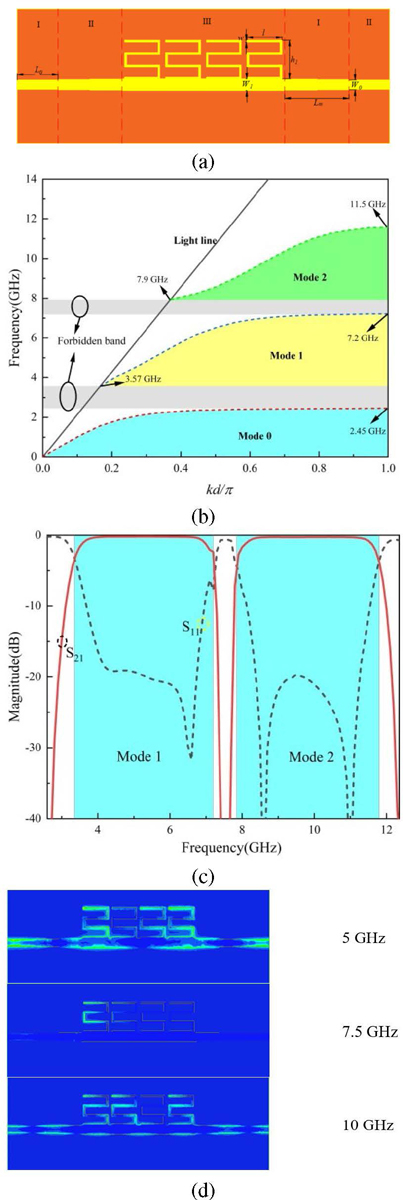
Figure 4: (a) Schematic diagram of the structure of the dual-band band-pass filter, (b) dispersion characteristics of the dual-band band-pass filter SSPPs cell structure, (c) S-parameters of the dual-band band-pass filter, and (d) electric field distributions of the dual-band band-pass filter at 5 GHz, 7.5 GHz, and 10 GHz.
In order to delve deeper into the characteristics of the bow-folded strip SSPPs structure at high-order mode, we piloted another dual-band band-pass filter design. The dimensions of the bow-folded strip cell structure are smaller, with a transverse dimension reduced to 70% of the conventional rectangular groove cell structure with h=22 mm. The total length of dual-band band-pass filter is 64 mm. Figure 4 (a) shows the schematic diagram of the dual-band band-pass filter structure, and Table 3 shows the optimized dimensions.
The dispersion curve of the dual-band band-pass filter cell structure is illustrated in Fig. 4 (b), and it can be seen that the groove depth clearly affects the total number of modes in the SSPPs structure, and there are two high-order mode. There is a forbidden band between the fundamental mode and the first high-order mode. There is also a forbidden band between the second high-order mode and the first high-order mode. The cut-off frequency for the first high-order mode is 7.2 GHz, whereas the cut-off frequency for the second high-order mode is 11.5 GHz. It is worth noting that the fundamental mode has a lower cut-off frequency compared to the single-band band-pass filter unit structure. By observing Fig. 4 (c), it becomes evident that two passbands are generated by the first high-order mode and the second high-order mode, covering the frequency ranges of 3.57-7.2 GHz and 7.9-11.5 GHz, respectively. These frequency ranges align with the dispersion curves illustrated in Fig. 4 (b). The first high-order mode demonstrates an insertion loss of below 0.2 dB, accompanied by a return loss better than 19 dB. Similarly, the second-order high mode shows an insertion loss lower than 0.3 dB and a return loss better than 19.5 dB. Consequently, the system exhibits a favorable response in terms of dual-band filtering.
In order to obtain a comprehensive understanding of the transmission characteristics, Fig. 4 (d) illustrates the distribution of electric fields at frequencies of 5, 7.5, and 10 GHz. At 5 GHz and 10 GHz passband range, the microstrip line effectively converts the guided wave into the SSPPs mode, resulting in a passband that exhibits excellent transmission performance. It is important to highlight that the electric field intensity is higher at 5 GHz compared to 10 GHz, indicating potential energy losses during transmission. At the blocking band frequency of 7.5 GHz, the majority of the electric field is concentrated on the initial SSPPs cell, resulting in the blocking of signals within the blocking band range.
Table 3: The optimized dimensions of dual-band band-pass filter (unit=mm)
| L | L | W | W | w | l | h |
|---|---|---|---|---|---|---|
| 7 | 11 | 1.55 | 2 | 0.3 | 6 | 6.6 |
Figure 5: (a) Fabricated samples of single-band band-pass filter, (b) fabricated samples of dual-band band-pass filter, (c) measured and simulated result of the single-band band-pass filter, (d) measured and simulated result of the dual-band band-pass filter, (e) comparison of simulated solder loss result for single-band band-pass filter with measured results, and (f) comparison of simulated solder loss result for dual-band band-pass filter with measured results.
IV. TEST RESULTS
In an effort to confirm the possibility of employing the high-order mode SSPPs band-pass filter, we fabricated and measured two distinct types of filters. Figures 5 (a) and (b) show the single-band and dual-band band-pass filters, correspondingly. This was achieved by taking into account the correlation between the high-order mode dispersion attributes of the proposed SSPPs cell and the geometric alteration of the slot. To acquire the S-parameters of the filter, we joined the filter with two SMA connectors. The connectors were used to connect the 50-ohm microstrip lines, and they were securely attached to both ends of two fabricated prototypes for the purpose of measurement. The results of the measurement are very similar to the simulation. As shown in Fig. 5 (c), the simulated return loss is better than 19 dB and the measured return loss is better than 10 dB in the passband from 4.8 GHz to 8 GHz, and the simulated return loss is better than 20 dB and the measured return loss is better than 10 dB in the passband from 8 GHz to 10.1 GHz. As shown in Fig. 5 (d), the simulated dual-band band-pass filter exhibits an insertion loss of less than 0.2 dB and a return loss better than 19 dB in the frequency range of 3.57 GHz to 7.2 GHz. Correspondingly, the measured dual-band band-pass filter showcases an insertion loss below 0.7 dB and a return loss greater than 14 dB in the identical frequency span. In the frequency range from 7.9 GHz to 11.5 GHz, the simulated dual-band band-pass filter attains an insertion loss below 0.3 dB and a return loss exceeding 19.5 dB. The measured dual-band band-pass filter exhibits an insertion loss less than 1dB and a return loss better than 10dB within the same frequency range.
It can be seen that the measured results match well with the simulation result curve, but the measured insertion loss and return loss are both higher than the simulation loss. This is mainly due to the SMA connector soldering and manufacturing tolerance. In order to reduce soldering loss, we can optimize the loss due to welding by simulating them before soldering, thus reducing the loss due to soldering during measurement. As shown in Figs. 5 (e) and (f), the S-parameters of the band-pass filter are simulated with the same environmental factors (with the same SMA connector and manufacturing tolerance) as in the measurement. It can be seen that the S-parameters of the single-band and dual-band band-pass filters with soldering loss agree with the curve fit of the measured S-parameters. Therefore, the soldering loss can be continuously optimized during the simulation process so that the simulation results can reach the best value to reduce the loss caused during soldering and make a better agreement between the measurement results and simulation results.
Table 4 presents a comparison of the performance and size of the band-pass filters proposed in this study with those previously reported based on the high-order mode of SSPPs. Both band-pass filters proposed in this research exhibit wider bandwidth fractions compared to the previously suggested filters. Compared to the single-band band-pass filters in [24, 27], the proposed single-band band-pass filter in this paper achieves a size reduction of nearly 50% while maintaining excellent performance. The proposed single-band band-pass filter has an insertion loss that is half of that in reference [23], and it also achieves a size reduction of nearly 67%. Compared to the single-band band-pass filters in [25], the proposed single-band band-pass filter demonstrates advantages in terms of insertion loss and size. With nearly identical dimensions, we have fabricated dual-frequency band-pass filters using first high-order mode and second high-order mode. According to Table 4, the size of the proposed dual-band band-pass filter is smaller than that of the dual-band band-pass filter of [26] and the performance of this filter is better.
Hence, both of the proposed band-pass filters possess the benefits of a compact structure and minimal insertion loss, and have potential application in integrated devices.
Table 4: Comparison of the proposed band-pass filters based on the high-order mode of SSPPs with the previous work
| Ref. | Number of Modes | (GHz) | IL(dB) | RL(dB) | Horizontal Dimension () | FBW(%) |
| [23] | Mode 1 | 11.5 | 2.3measured | 10measured | 0.59 | 56.5 |
| [24] | Mode 1 | 7.79 | 1.46measured | 10measured | 0.39 | 43.4 |
| [25] | Mode 1 | 8 | 1.7measured | 12measured | 0.24 | 50 |
| [26] | Mode 1Mode 2 | 7.95, 14.65 | 0.2, 0.36simulated | 15,15simulated | 0.2,0.36 | 64.229.4 |
| [27] | Mode 1 | 8.2 | 0.16simulated | 12.6simulated | 0.47 | 58 |
| This work | Mode 1 | 7.5 | 0.3simulated1measured | 14simulated10measure | 0.2 | 78.5 |
| Mode 1Mode 2 | 5.4,9.7 | 0.2, 0.3simulated0.7, 1measured | 19, 19.5simulated14, 10measured | 0.15, 0.27 | 67.237.1 |
V. CONCLUSION
In this paper, we design two types of band-pass filters: single-band and dual-band filters. These filters utilize the high-order mode of spoof surface plasmon polaritons as their foundation. Compared to the conventional single-side rectangular groove SSPPs cell, our proposed cells reduce the electrical size by 59% and 70% at the same high-order cut-off frequency. By simulating the dispersion curves of the SSPPs cell structure, we examine the primary parameters that impact the cut-off frequency of both the fundamental and high-order mode of SSPPs. The simulation and measurement of the single-band and dual-band band-pass filters, which are based on the high-order mode of SSPPs with a bow-folded strip structure, are performed using microstrip line feed. The simulation results align well with the measured results, demonstrating the feasibility of applying the SSPPs high-order mode to band-pass filter design. We also verified the key factors that cause a slight difference between the measured and simulated results. The simplicity and small size of the proposed structure and design method suggest promising potential applications in plasma devices and systems.
ACKNOWLEDGMENT
This work was Supported by Natural Science Foundation of Sichuan Province (No.2022NSFSC0332), Backbone teachers Program under grant 10912- JXGG2021-06751, grant SWPTJG2102 and the Backbone teachers Program under grant 10912- JXGG2022- 01782.
REFERENCES
[1] W. L. Barnes, A. Dereux, and T. W. Ebbesen, “Surface plasmon subwave length optics,” Nature, vol. 424, no. 6950, pp. 824-830, Aug. 2003.
[2] J. B. Pendry, L. Martín-Moreno, and F. J. Garcia-Vidal, “Mimicking surface plasmons with structured surfaces,” Science, vol. 305, no. 5685, pp. 847-848, 2004.
[3] F. J. Garcia-Vidal, L. Martín-Moreno, and J. B. Pendry, “Surfaces with holes in them: New plasmonic metamaterials,” Journal of Optics A: Pure and Applied Optics, vol. 7, no. 2, pp. S97-S101, 2005.
[4] X. P. Shen, T. J. Cui, D. Martin-Cano, and F. J. Garcia-Vidal, “Conformal surface plasmons propagating on ultrathin and flexible films,” Proc. Nat. Acad. Sci. USA, vol. 110, no. 1, pp. 40-45, Jan. 2013.
[5] H. F. Ma, X. Shen, Q. Cheng, W. X. Jiang, and T. J. Cui, “Planar plasmonic metamaterial on a thin film with nearly zero thickness,” Applied Physics Letters, vol. 102, no. 21, p. 211909, 2013.
[6] L. F. Ye, Y. F. Xiao, and N. Liu, “Plasmonic waveguide with folded stubs for highly confined terahertz propagation and concentration,” Optics Express, vol. 25, no. 2, pp. 898-906, 2017.
[7] W. Feng, Y. Feng, W. Y. Ang, W. Che, and Q. Xue, “High-performance filtering antenna using spoof surface plasmon polaritons,” IEEE Trans. Plasma Sci., vol. 47, no. 6, pp. 2832-2837, June 2019.
[8] E. Mohamed, K. M. Ibrahim, and A. M. Attiya, “Analysis and design of a diplexer for satellite communication system,” Applied Computational Electromagnetics Society (ACES) Journal, vol. 35, no. 10, pp. 1236-1241, 2020.
[9] R. S. Anwar, L. Mao, and H. Ning, “Role of surface geometric patterns and parameters in the dispersion relations of spoof surface plasmon polaritons at microwave frequency,” Applied Computational Electromagnetics Society (ACES) Journal, vol. 34, no. 1, pp. 172-179, 2021.
[10] Y. J. Guo, K. D. Xu, Y. H. Liu, and X. H. Tang, “Novel surface plasmon polariton waveguides with enhanced field confinement for microwave-frequency ultra-wideband bandpass filters,” IEEE Access, vol. 6, pp. 10249-10256, Feb. 2018.
[11] K.-D. Xu, F. Zhang, Y. Guo, L. Ye, and Y. Liu, “Spoof surface plasmon polaritons based on balanced coplanar stripline waveguides,” IEEE Photon. Technol. Lett., vol. 32, no. 1, pp. 55-58, Jan. 2020.
[12] H. L. Zhu, Y. Zhang, and L. F. Ye, “Compact terahertz on-chip filter with broadband rejection based on spoof surface plasmon polaritons,” IEEE Electron Device Letters, vol. 43, no. 6, pp. 970-973, June 2022.
[13] S. Sun, Y. Cheng, and H. Luo, “Notched-wideband bandpass filter based on spoof surface plasmon polaritons loaded with resonator structure,” Plasmonics, pp. 165-174, 2023.
[14] L. Ye, Z. Chen, Y. Zhang, W. Li, Y. Zhang, and K. Wei, “High performance multiple passband substrate integrated plasmonic filters,” IEEE Transactions on Circuits and Systems II: Express Briefs, vol. 70, no. 4, pp. 1445-1449, Apr. 2023.
[15] Y. J. Guo, K. D. Xu, X. Deng, X. Cheng, and Q. Chen, “Millimeter wave on-chip bandpass filter based on spoof surface plasmon polaritons,” IEEE Electron Device Lett., vol. 41, no. 8, pp. 1165-1168, Aug. 2020.
[16] W. Feng, Y. Feng, W. Y. Ang, W. Che, and Q. Xue, “High-performance filtering antenna using spoof surface plasmon polaritons,” IEEE Trans. Plasma Sci., vol. 47, no. 6, pp. 2832-2837, June 2019.
[17] X. F. Zhang, J. Fan, and J. X. Chen, “High gain and high-efficiency millimeter-wave antenna based on spoof surface plasmon polaritons,” IEEE Trans. Antennas Propag., vol. 67, no. 1, pp. 687-691, Jan. 2019.
[18] J. Wang, L. Zhao, Z. C. Hao, X. P. Shen, and T. J. Cui, “Splitting spoof surface plasmon polaritons to different directions with high efficiency in ultra-wideband frequencies,” Opt. Lett., vol. 44, no. 13, pp. 3374-3377, July 2019.
[19] X. Gao, J. H. Shi, X. P. Shen, H. F. Ma, W. X. Jiang, L. Li, and T. J. Cui, “Ultrathin dual-band surface plasmonic polariton waveguide and frequency splitter in microwave frequencies,” Appl. Phys. Lett., vol. 102, no. 15, Art. no. 151912, Apr. 2013.
[20] B. C. Pan, P. Yu, Z. Liao, F. Zhu, and G. Q. Luo, “A compact filtering power divider based on spoof surface plasmon polaritons and substrate integrated waveguide,” IEEE Microwave and Wireless Components Letters, vol. 32, no. 2, pp. 101-104, Feb. 2022.
[21] C. Han, Z. H. Wang, Y. Y. Chu, X. D. Zhao, and X. R. Zhang, “Compact flexible multifrequency splitter based on plasmonic graded metallic grating arc waveguide,” Opt. Lett., vol. 43, no. 8, pp. 1898-1901, 2018.
[22] D. Yi, X. C. Wei, and R. Yang, “Modeling and analyzing high-order modes in periodic-stub-loaded stripline for wideband filter design,” IEEE Transactions on Electromagnetic Compatibility, Vol. 62, no. 2, pp. 398-405, 2020.
[23] Y. Liu and K. D. Xu, “Bandpass filters using grounded stub-loaded microstrip periodic structure for suppression of modes,” Journal of Physics D: Applied Physics, vol. 55, no. 42, p. 425104, 2022.
[24] Y. Liu, K. D. Xu, Y. J. Guo, and Q. Chen, “High-order mode application of spoof surface plasmon polaritons in bandpass filter design,” IEEE Photonics Technology Letters, vol. 33, no. 7, pp. 362-365, 2021.
[25] Z. Lin, Y. Li, L. Li, Y. T. Zhao, J. Xu, and J. Chen, “Miniaturized bandpass filter based on high-order mode of spoof surface plasmon polaritons loaded with capacitor,” IEEE Transactions on Plasma Science, vol. 51, no. 1, pp. 254-260, Jan. 2023.
[26] S. Zhu, P. Wen, and Y. Liu, “Multi-band propagation of spoof surface plasmon polaritons by its high-order modes,” Japanese Journal of Applied Physics, vol. 61, no. 7, p. 070907, 2022.
[27] Y. Liu, K. D. Xu, Y. J. Guo, and Q. Chen, “High-order mode of spoof surface plasmon polaritons and its application in bandpass filters,” IEEE Transactions on Plasma Science, vol. 49, no. 1, pp. 269-275, 2021.
[28] H. H. Zhao, P. Zhou, Z. Xu, S. Li, and X. Yin, “Tri-band band-pass filter based on multi-mode spoof surface plasmon polaritons,” IEEE Access, vol. 8, pp. 14767-14776, 2020.
[29] W. Feng, S. Shi, S. Yin, H. Zhu, Y. Shi, and W. Che, “Novel wideband bandpass filters using double-sided quasi-SSPPs transmission line,” IEEE Transactions on Circuits and Systems II: Express Briefs, vol. 69, no. 7, pp. 3174-3178, July 2022.
[30] X. Liu, Y. Feng, B. Zhu, J. Zhao, and T. Jiang, “High-order modes of spoof surface plasmonic wave transmission on thin metal film structure,” Opt. Exp., vol. 21, no. 25, pp. 31155-31165, 2013.
[31] H. C. Zhang, “Fundamental theory, device synthesis and system integration of spoof surface plasmon polaritons,” dissertation, Nanjing: Southeast University, 2020.
BIOGRAPHIES

Siyu Yang is studying for the master’s degree at Chengdu University of Technology, Chengdu, China. Her current research interests include Spoof Surface Plasmon Polaritons and microwave circuits.

Shuang Liu received the PhD. degree in electromagnetic field and microwave technology from University of Electronic Science and Technology of China (UESTC), Chengdu, China, in 2016. She is currently a teacher in Chengdu University of Technology, Chengdu, China. Her current research interests include microwave, millimeter-wave and terahertz passive circuits, antenna, spoof surface plasmon polaritons, and physics.

Huali Zhu received the B.S. degree from the University of Electronic Science and Technology of China, Chengdu, China, in 2017. He is currently pursuing the Ph.D. degree with the University of Electronic Science and Technology of China, Chengdu, China, majoring in electronic science and technology. His current research interests include microwave/millimeter wave circuit theory and technology, mm-wave and terahertz integrated circuits and systems.

Fachun He is studying for the master’s degree at Chengdu University of Technology, Chengdu, China. His current research interests include spoof surface plasmon polaritons and microwave circuits.

Dan Lei received the B.S. degree in applied physics from Chongqing University in 2000, M.Eng. in electromagnetic field and Microwave Technology from University of Electronic Science and Technology of China in 2007. She is currently teaching electrodynamics and microwave technology and antennas at Chengdu University of Technology. Her current research interests include numerical modeling methods of passive microwave circuits, microwave circuits and microwave test.

Jun Yan received the S. and Ph.D. degrees in electromagnetic and microwave engineering from the University of Electronic Science and Technology of China, Chengdu, China, in 2005 and 2016, respectively. He is currently an Engineer of microwave engineering at the China Electronics Technology Group Corporation 10th Research Institute, Chengdu. His research interests include wide-band, low-profile antenna array and feed-network design for microwave and millimeter-wave frequencies.

Chan Gao received the B.S. degree in applied physics from Henan University of Technology, Zhengzhou, China in 2012, and the Ph.D. degree in condensed matter physics from University of Science and Technology of China (USTC), Hefei, China, in 2018. From 2018-2021, she was a postdoctoral researcher in University of Science and Technology of China (USTC), Hefei, China. She is currently a lecturer in Chengdu University of Technology (CDUT), Chengdu, China. Her current research interests include the structure and photoelectrical properties of material under extreme condition and microwave circuits.
ACES JOURNAL, Vol. 39, No. 4, 297–306
doi: 10.13052/2024.ACES.J.390403
© 2024 River Publishers

