A Miniaturized C-B and SIW Bandpass Filter based on LTCC
Wei Tang, Ruo-Feng Xu, and Lei Zhao
1School of Information and Control Engineering, China University of Mining and Technology
Xuzhou, Jiangsu, 221116, China
weitangmax@163.com, xuruofeng@cumt.edu.cn, leizhao@cumt.edu.cn
Submitted On: April 3, 2023; Accepted On: July 8, 2023
ABSTRACT
In this paper, a miniaturized bandpass filter based on low temperature co-fired ceramic (LTCC) technology is proposed. The miniaturization is achieved by two double folded substrate integrated waveguide (DFSIW) resonant cavities. By interconnecting LTCC three-dimensional structure, the resonant cavities can be stacked vertically. Compared with the conventional SIW filter, the size is reduced by 75.6%. The experimental results show that the low insertion loss and good selectivity are achieved. The proposed miniaturized bandpass filter is promising for 5G application.
Index Terms: Bandpass filter, double folded substrate integrated waveguide, folded waveguide resonator, low temperature co-fired ceramic (LTCC), resonant cavity.
I. INTRODUCTION
In modern satellite and mobile communication systems, there is a growing demand for low insertion loss, compact and easy-to-integrate bandpass filters. However, the conventional rectangular waveguide filter in C-Band has the dimensional limitation, which is difficult to integrate with planar circuits. A number of literatures have been studied on the nature of substrate integrated waveguide (SIW) cavities for the design of miniaturized filters [1–2], but the size reduction cannot satisfy the rapid development of modern wireless communication systems.
Nowadays, low temperature co-fired ceramic (LTCC) technology has been widely used in the design of compact components because of its high-density packaging and 3-D integration. It can be seen as the further miniaturization for compact filter processing on the basis of printed circuit board (PCB) technology [3]. In [4], a vertical LTCC rectangular waveguide bandpass filter with compact size and 2.1 dB insertion loss is proposed by using dielectric cavities. In [5], a multilayer SIW filter based on LTCC technology is designed, which uses a vertical structure to reduce the size. Although the LTCC technology with building the resonant cavities vertically can reduce its planar area, the size of the cross-section is still quite large and the insertion loss rises as the stacks increase.
To further reduce the cross-section of filters, the folded substrate integrated waveguide (FSIW) technology had been introduced [6]. The folding technology could effectively apply to design the compact structure in LTCC. Some miniaturized bandpass LTCC filters were proposed [7–8], which used the FSIW cavity to realize half the planar size of the structure. For earing more miniaturization spaces, a double folding substrate integrated waveguide (DFSIW) was applied to design three-order Chebyshev bandpass filters [9]. However, the insertion losses were quite large for realisticapplications.
In the LTCC process, well-designed circuits and materials are important parts of key issues to cut down losses. For a single layer SIW cavity, the filtering circuits were optimized by etching different sizes of slots [10], which formed three resonance cavities and led to the minimum loss of 1.913 dB. In [11], a bandpass SIW filter using U-shape slots is proposed, and an electromagnetic band gap (EBG) was put into the structure to enhance the filtering performance and reduce the loss, which was only 1.42 dB at the center frequency. The one-layer structures are easily optimized to lower the loss, but hybrid coupling effects occur between cells, which may cause the loss difficult to control for a folding filter with multiple layers.
In [12], a new type of H-plane FSIW filter is presented. Multi-layer FSIW resonators and I/O sections were linked by the evanescent SIW sections, which eliminated the loss of extra vias. But the lowest insertion loss was 2.6 dB. In the meantime, silver as the conductor was used in the construction of SIW cavities, which had the practical impacts on the loss control [13]. Although these attempts on the loss reduction based on LTCC had a few progresses, the passband loss was still relatively high and there is few recent research combined with the folding technology. Thus, it is quite a challenge to design a FSIW bandpass filter using LTCC technology in C-Band with compact size and very low loss.
In this paper, a compact bandpass filter with low insertion loss is proposed. The filter is designed with DFSIW resonant cavity, and achieved greater miniaturization with the LTCC packaging process in C-Band. Based on the field distribution characteristics of SIW mode, the magnetic coupling is adopted between adjacent SIW resonators. In order to meet the test requirement, the ground coplanar waveguide (GCPW) is used to design the feed line. The fabricated and measured results are well matched.
Figure 1: Design structure of the filter: (a) 3-D view, (b) the top view of feed part, (c) couple layer, and (d) the top view of a DFSIW resonator.
II. FILTER DESIGN
A. Filter geometry
The three-dimensional structure of the filter is shown in Fig. 1 (a). The filter consists of metal layers, substrate layers, and via arrays as vertical sidewalls. The top and bottom metal layers connect the GCPW as feeding lines of the filter, which is shown in Fig. 1 (b). The input and output GCPWs are orthogonal to avoid interactions. Two double-folded SIW resonators are vertically placed, which are coupled through a slot in couple layer. Figure 1 (c) shows the construction of this layer. The metal layer 2 and metal layer 4 are coupling layers of the DFSIW resonator, which are shown in Fig. 1 (d). There is a right-angle slot in each metal layer, which is close to the sidewall.
Ferro-A6 is used as substrates in the structure, which has the dielectric constantand loss tangent , respectively. The thickness of each dielectric layer is 0.2 mm. The parameters of the filter are shown in Table 1.
Table 1: Units for magnetic properties
| Variable | Value (mm) | Variable | Value (mm) |
|---|---|---|---|
| d | 0.15 | p | 0.3 |
| l | 8 | w | 0.4 |
| l | 6 | w | 0.6 |
| l | 5.15 | w | 0.2 |
| l | 1.74 | w | 0.5 |
The coupling matrix of the designed filter operating at 4.9 GHz is shown in Equation (1):
| (1) |
B. DFSIW cavity design
The TEmode in the SIW cavity is similar to the corresponding mode of conventional rectangular metal waveguides. Therefore, the SIW cavity size can be determined by [14]
| (2) |
and
| (3) |
in which cis the speed of light. The a and b are the effective width and length of the SIW cavity, and its value can be obtained by the formula (3). Here, and represent the diameter of the metallized vias and the distance of adjacent vias, a and b represent the actual width and length of the SIW cavity, respectively. When the resonant frequency of the SIW cavity is 4.9 GHz, the conventional SIW cavity size is 17.8217.82 0.2 mm.
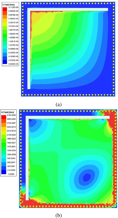
Figure 2: Field plot: (a) Electric field distributions of a quarter DFSIW cavity and (b) magnetic field distributions of a quarter DFSIW cavity.
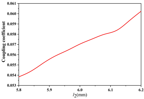
Figure 3: Coupling coefficients and slot length.
In the conventional TEmode of the SIW resonator, the strongest electric field is distributed in the center of cavity, and the magnetic field distribution reaches maximum at the edge. Figure 2 shows the E-field and M-field distributions in the TEmode of the designed DFSIW resonator. It can be observed that the electric field is the strongest along the right-angle slot, and the magnetic field is centrally distributed at the end of the slot. Through the folding technology, the positions of field distributions are changed, but the TEmode is still maintained by the DFSIW resonator. As the folding structure is achieved through the SIW folded twice along the right-angle slot, each side of the DFSIW resonator is reduced by half. The thickness of one DFSIW resonator is double that of the SIW cavity. Therefore, the size of designed cavities is theoretically 8.918.91 0.4 mm.
C. DFSIW filter coupling structure
The magnetic coupling mode is adopted between the folded resonant cavities. The slot in the coupling layer is placed near the sidewall. Due to the manufacturing limitations, the position of the coupling slot is 0.65 mm from the vias. By adjusting the position and size of the slot, the coupling strength can be controlled. In Fig. 3, the relationship between the length of slot and coupling coefficient is shown. When the length of the coupling slot increases, the coupling coefficient rises. To meet the requirement of the filter, the length of the coupling slot is chosen as 6 mm.
The insertion loss in the passband mainly consists of the dielectric and conductor loss. To reduce the conductor loss, silver is used to form the metal layer due to its low conductivity. The excellent LTCC processes ensure that each metal layer is only 0.008 mm, and the thickness of the whole dielectric layer is 0.8 mm.
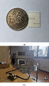
Figure 4: (a) Fabricated filter and (b) test platform.
III. SIMULATION AND TESTING
The designed filter is simulated by high frequency structure simulator (HFSS), and the actual size of the structure is 8.88.80.816 mm. The simulated values of the DFSIW cavity are consistent with the theoretical ones. The filter is fabricated by multi-layer LTCC technology, and the production is shown in Fig. 4 (a). The experimental test was completed at the State Key Laboratory of Millimeter Wave in Southeast University. The sample was tested in an Agilent E8363B vector network analyzer, and the platform is shown in Fig. 4 (b).
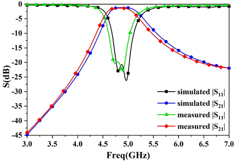
Figure 5 shows that the simulated and fabricated results are well matched. The measured center frequency is 4.95 GHz, with insertion loss of 1.17 dB. The 3 dB passband ranges from 4.57 GHz to 5.12 GHz, with a relative bandwidth of 11%. In addition, the return loss is better than 10 dB over the range of 4.48-5.36 GHz. Compared with the simulation, the test results have 0.05 GHz center frequency shift, which may be caused by parasitic inductance.
Figure 5: Simulated and measured S parameters.
Table 2: Comparison of the proposed filter with other filters
| Ref. | f(GHz) | IL (dB) | Size () |
|---|---|---|---|
| [8] | 5 | 3.48 | 0.720.37 |
| [15] | 4.97 | 2.2 | 1.281.30 |
| This work | 4.9 | 1.17 | 0.350.35 |
In Table 2, the performance of the designed filter is compared with other SIW filters. From the comparison results, the filter designed in this paper has a lower insertion loss and a smaller size.
IV. CONCLUSION
In this paper, a novel DFSIW bandpass filter based on LTCC technology is demonstrated. The structure and the coupling principle of DFSIW resonators are well described, which achieve 75.6% size reduction comparing with the conventional SIW filters. Meanwhile, the LTCC filter is fabricated and measured at C-band with very low insertion loss. The great size reduction is realized by the double folding resonators, and low-loss bandpass performance is achieved by the well-designed coupling position through LTCC technology. The proposed filter has the extensive application in the sub-band of 5G systems.
REFERENCES
[1] Y. Cassivi, L. Perregrini, P. Arcioni, M. Bressan, K. Wu, and G. Conciauro, “Dispersion characteristics of substrate integrated rectangular waveguide,” IEEE Microw. Wireless Compon. Lett., vol. 12, no. 9, pp. 333-335, Sep. 2002.
[2] Y. L. Zhang, W. Hong, F. Xu, K. Wu, and Tie Jun Cui, “Analysis of guided-wave problems in substrate integrated waveguides numerical simulations and experimental results,” IEEE MTT-S Int. Microwave Symp. Dig., pp. 2049-2052, Jan. 2003.
[3] Y. Rao, H. J. Qian, J. Zhou, Y. Dong, and X. Luo, “Miniaturized 28-GHz packaged bandpass filter with high selectivity and wide stopband using multilayer PCB technology,” IEEE Microw. Wireless Compon., Lett., vol. 32, no. 6, pp. 664-667, June 2022.
[4] A. Isapour and A. Kouki, “Vertical LTCC integrated rectangular waveguide and transitions for millimeter-wave applications,” IEEE Trans.Microw. Theory Techn., vol. 67, no. 3, pp. 868-882, Mar. 2019.
[5] K. S. Chin, C. C. Chang, C. H. Chen, Z. Guo, D. Wang, and W. Che, “LTCC multilayered substrate-integrated waveguide filter with enhanced frequency selectivity for system-in-package applications,” IEEE Trans. Compon., Packag. Manuf. Technol., vol. 4, no. 4, pp. 664-672, Apr. 2014.
[6] J. S. Hong, “Compact folded waveguide resonator,” in IEEE MTT-S Int. Microw. Symp. Dig., pp. 213-216, June 2004.
[7] Y. Fei, L. Rui-zhu, Y. Hong-xi, H. Xin-yang, and Z. Ying, “Miniaturized folded substrate integrated waveguide filters in LTCC,” 2011 IEEE International Conference on Microwave Technology & Computational Electromagnetics, Beijing, China, 2011, pp. 171-173, 2011.
[8] L. F. Qiu, B. Xie, L. S. Wu, and J. F. Mao, “A flat-passband predistorted bandpass filter with folded substrate integrated waveguide,” IEEE Transactions on Circuits and Systems—II: Express Briefs., vol. 69, no. 2, pp. 324-328, Feb. 2022.
[9] H. Y Chien, T. M. Shen, T. Y. Huang, W. H. Wang, and R. B. Wu, “Miniaturized bandpass filters with double-folded substrate integrated waveguide resonators in LTCC,” IEEE Trans. Microw. Theory Techn., vol. 57, no. 7, pp. 1774-1782, July 2009.
[10] S. W. Wong, R. S. Chen, K. Wang, Z. N. Chen, and Q. X. Chu, “U-shape slots structure on substrate integrated waveguide for 40-GHz bandpass filter using LTCC technology,” IEEE Trans. Compon. Packag. Manuf. Technol., vol. 5, no. 1, pp. 128-134, Jan. 2015.
[11] S. W. Wong, K. Wang, Z. N. Chen, and Q. X. Chu, “Design of millimeter-wave bandpass filter using electric coupling of substrate integrated waveguide (SIW),” in IEEE Microwave and Wireless Components Letters, vol. 24, no. 1, pp. 26-28, Jan. 2014.
[12] L. S. Wu, X. L. Zhou, and W. Y. Yin, “A novel multilayer partial H-plane filter implemented with folded substrate integrated waveguide (FSIW),” in IEEE Microwave and Wireless Components Letters., vol. 19, no. 8, pp. 494-496, Aug. 2009.
[13] Y. Li, L. A. Yang, L. Du, K. Z. Zhang, and Y. Hao, “Design of millimeter-wave resonant cavity and filter using 3-D substrate-integrated circular waveguide,” IEEE Microw. Wireless Compon., Lett., vol. 27, no. 8, pp. 706-708, Aug. 2017.
[14] Y. Cassivi and K. Wu, “Low-cost microwave oscillator using substrate integrated waveguide cavity,” IEEE Microw. Wireless Compon. Lett., vol. 13, no. 2, pp. 48-50, Feb. 2003.
[15] L. F. Qiu, L. S. Wu, B. Xie, W. Y. Yin, and J. F. Mao, “Substrate integrated waveguide filter with flat passband based on complex couplings,” IEEE Microwave and Wireless Components Letters, vol. 28, no. 6, pp. 494-496, June 2018.
BIOGRAPHIES

Wei Tang Master’s degree student in School of Information and Control Engineering, China University of Mining and Technology, major research interests are SIW filter, active adjustable filter, etc.

Ruofeng Xu received the B.SC. (2004) degree from Suzhou University in electronics and Sscience and technology, and received M.Sc. (2006) and Ph.D. (2010) degrees in electronic engineering from the University of Kent, UK. He was a visiting scholar (2018) for one year in Rutgers University, USA. Now he is a lecturer in School of Information and Control Engineering, China University of Mining and Technology. His main research directions are microwave technology andapplication.

Lei Zhao (M’09–SM’18) received the B.S. degree in mathematics from Jiangsu Normal University, China, 1997, the M.S. degree in computational mathematics, and the Ph.D. degree in electromagnetic fields and microwave technology from Southeast University, Nanjing, China, in 2004 and 2007, respectively. Zhao serves as an associate editor for IEEE Access, an associate editor-in-chief for ACES Journal, and a reviewer for multiple journals and conferences including the IEEE Trans. on Microwave Theory and Techniques, IEEE Trans. Antennas and Propagation, IEEE Access, IEEE Antennas and Wireless Propagation Letters, ACES Journal, and other primary electromagnetics and microwave relatedjournals.
ACES JOURNAL, Vol. 38, No. 9, 741–745
doi: 10.13052/2023.ACES.J.380915
© 2023 River Publishers

