Design of a Retransmitted Chipless Tag based on Multi-state Resonators
Nengyu Huang and Zhonghua Ma
1School of Ocean Information Engineering
Jimei University, Xiamen, Fujian 361021, China
mzhxm@jmu.edu.cn
2School of Navigation
Jimei University, Xiamen, Fujian 361021, China
huangny05@163.com
Submitted On: May 21, 2021; Accepted On: October 18, 2021
ABSTRACT
In order to increase the encoding capacity and reduce the size of the tag, this paper proposes the frequency sharing method to design a retransmitted chipless tag, which is composed of N resonators, a coupled microstrip transmission line, and the orthogonal transmitting antenna and receiving antenna. A pair of the same size resonators is placed symmetrically on both sides of the coupled microstrip transmission line. M open-ended stubs (OES) with different combinations are embedded in each resonator to obtain different resonance frequencies. The frequency sharing multi-state resonators’ chipless tags are designed where N=6, M=4, and the dimension of the tag is 46 mm 30 mm, which can generate about 2 codes. Simulation and measurement results show good agreement and feasibility of the tag design. The chipless tag is small in size, has large encoding capacity and is easy to print. This kind of tag has no silicon chip so the cost is low. It can be widely used in logistics, supermarkets and other fields to replace the barcode.
Index Terms: chipless tag, encoding capacity, frequency sharing, radio frequency identification, resonator.
I. INTRODUCTION
The Radio Frequency Identification (RFID) system is one of the core technologies in the field of the Internet of Things (IoT), which is mainly composed of a reader and tags. The reader is composed of a continuous wave transmitting circuit, a modulated wave receiving circuit, and reader antennas to extract the tag’s identification (ID) and other data information. The tag is a data carrier that includes a tag antenna and silicon chip [1]. Once the reader is put into use, it does not need to be replaced, so its cost is fixed. However, the tags are attached to items so the quantity is huge. All of the tags are read by the same reader, so the cost reduction of the RFID system mainly depends on the cost of the tags [2]. The cost of the traditional chip-tags mainly depends on the cost of the silicon chip. The cost of silicon material and the production process of the chip are fixed, so the cost of the chip cannot be cut down. The high cost is the key obstacle for the application of the traditional chipped tag in low-price commodities (such as stamps, tickets and envelopes, etc.) [3]. Therefore, many scholars have begun to design chipless tags. The cost of chipless tags depends on the cost of the conductive material that constitutes the resonant circuits. Due to removing the tag’s silicon chip, the cost of the chipless tag is drastically reduced, but it has the advantages of traditional chip tags, such as non-line-of-sight (NLOS) reading and automatic identification. This chipless tag system can also work under extreme conditions (such as high temperature and high humidity, etc.). However, it has deficiencies in terms of data capacity and tag size when compared with the traditionaltags [4, 5].
Usually chipless tags are divided into two categories: time-domain (TD) [6–12] and frequency-domain (FD) [3, 13–24]. The TD chipless tag is mainly composed of two types, i.e. transmission delay line and surface acoustic wave (SAW) filter. The transmission delay line chipless tag works at the nanosecond level. Signal detection is difficult. At the same time, the encoding capacity is small, only one or a few bits. It is mainly used in anti-theft, access control, etc. [6]. Although a SAW chipless tag has high encoding capacity, it requires high-cost piezoelectric materials and cannot be printed directly [7]. Compared with the TD-based chipless solutions, the FD-based chipless tag has many advantages. In addition to easier signal detection and lower cost of the tag, it also potentially has a larger encoding capacity depending on the tag size andavailable spectrum.
Chipless tags based on the FD have two working methods: chipless tags extracting Radar Cross Section (RCS) spectrum characteristics [13–17] and retransmitted chipless tags [3, 18–24]. The chipless tag based on RCS does not require receiving and transmitting antennas, and its RCS spectrum structure is responsible for loading the encoded information. The tag’s encoding capacity is increased by adding resonators, but the coupling effect will be introduced at the same time. Theoretically, the reading distance of the RCS chipless tag will be very far, but it is limited by its actual environment and requires a complicated algorithm to separate the RCS signal of the tag in order to decode it. Moreover, other interference may also be introduced in a complex environment, so the chipless tag needs constant calibration. The retransmitted chipless tag requires two orthogonal ultra-wideband (UWB) antennas and relevant resonator circuits. The transmitting and receiving antennas are orthogonally polarized to each other. There is no interference between the receiving signal and transmitting signal of the tag, so the reader has the low bit error rate when reading chipless tags. The reading distance is further than the RCS chipless tag in the actual environment. The number of the traditional retransmitted chipless tag resonators is the same as the number of data bits. Increasing encoding capacity can be implemented by adding the number of resonators. The coupling effect between the resonators can be reduced by adjusting resonator intervals. Previous papers [3, 18] have proposed a 6-bit retransmitted chipless tag with spiral resonators. As the number of spiral resonators increased to 35, the encoding capacity is increased to 35 bits. Furthermore, the size of this chipless tag isenlarged correspondingly.
In order to improve the encoding capacity without increasing the dimension of the tag, the retransmitted chipless tag is proposed in this paper which is composed of frequency sharing multi-state resonators, wherein each resonator can provide more than two states. By using the sharing frequency method, the tag can provide larger encoding capacity with a smaller number of resonators. There is a ground plate on the back of the tag which can isolate the influence of the adhesive objects on the tag’s performance. Chipless tags with a retransmitted structure have high sensitivity and long reading distance due to the gain of the antenna and the non-interference between the receiving and transmitting signals of the tag. The communication distance of the chipless tag with this structure is 30 cm. The tag can be widely used in logistics, supermarkets and other fields to replacethe barcode.
II. WORKING PRINCIPLE OF THE RETRANSMISSION CHIPLESS TAG
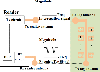
Figure 1 is the working principle diagram of the retransmission chipless tag with multi-state sharing frequency resonators. The tag includes a vertically polarized receiving antenna, a horizontally polarized transmitting antenna, multi-state resonators and a coupled microstrip transmission line. The transmitting antenna of the reader transmits the UWB interrogation signal with a uniform spectrum to the chipless tag, and the receiving antenna of the tag receives the UWB interrogation signal and transfers it to the multi-state resonator coupling circuits by the microstrip transmission line. The multi-state resonator coupling circuits adopt cascaded multi-state resonators with M embedded OES to encode the data, which forms a series of spectral signatures in the UWB signal spectrum. At the same time, the data of the chipless tag is loaded into the spectral signatures of the UWB signal. The transmitting antenna of the chipless tag retransmits this UWB signal with encoded spectrum signatures back to the reader; then, the data information can be obtained by the decoding circuit and certain algorithms. The receiving and transmitting antennas of the reader are also orthogonally polarized to avoid the mutual interference between the transmitted signal and the received encoded signal in the reader. The transmitting antenna of the reader and the receiving antenna of the tag have the same polarization characteristic, and the receiving antenna of the reader and the transmitting antenna of the tag have the same polarization characteristic.
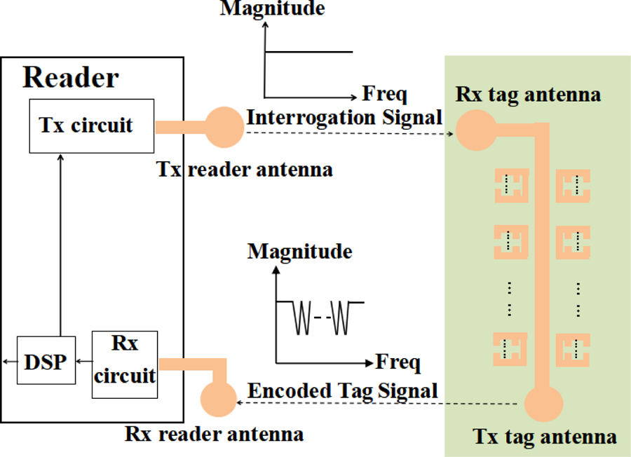
Figure 1: Working principle of the retransmitted chipless tag with multi-state sharing frequency resonators.
III. SIMULATION DESIGN
Figure 2 is the structural parameter diagram of the multi-state resonators of M=4. W is the width of the coupled microstrip transmission line, t is the longitudinal interval between the embedded OES, and g and w are the length and width of the OES, respectively. The length and width of all embedded OES are equal. d is the distance between the resonator and the coupled microstrip transmission line, and d is the distance between adjacent resonators. The RO4350 dielectric substrate has low loss, reasonable cost, small circuit size, good stability and consistency compared with other microwave substrates. The dielectric constant of 3.66 makes the circuit size not too large. The thickness of substrate is 0.508 mm, and a thin substrate can reduce the surface waves. Therefore, Rogers microwave board RO4350 (with =3.66, tan =0.004, h=0.508 mm) is selected as thesubstrate.
This chipless tag can also be printed directly on other low-cost dielectric substrates, such as packaging cartons, plastic bottles or glass. But the size of the resonator needs to be adjusted and the coding rules are not affected.
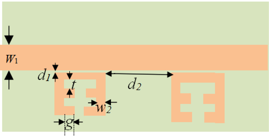
Figure 2: Structural parameters diagram of the multi-state resonators.
The characteristic impedance Z of a single microstrip line in a homogeneous medium is expressed as follows [25]:
| (1) |
| (2) |
where is the effective dielectric constant, , is the wave impedance in free space, u is the ratio of the width of the microstrip to the height of the substrate (u=W/ h), F is a value related to the u, and
| (3) |
where is the relative dielectric constant, a is a value related to u, and b is a value related to relative dielectric . The accuracy of this expression applies to 128 and 0.01 u 10. The equations of a and b are as follows [26]:
| (4) |
| (5) |
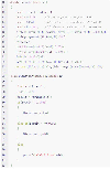
From equation (1), the thickness of the dielectric substrate h=0.508 mm and the relative dielectric constant =3.66, then the width (W) of the Z=50 microstrip transmission line can be obtained by the program code shown in Fig. 3.
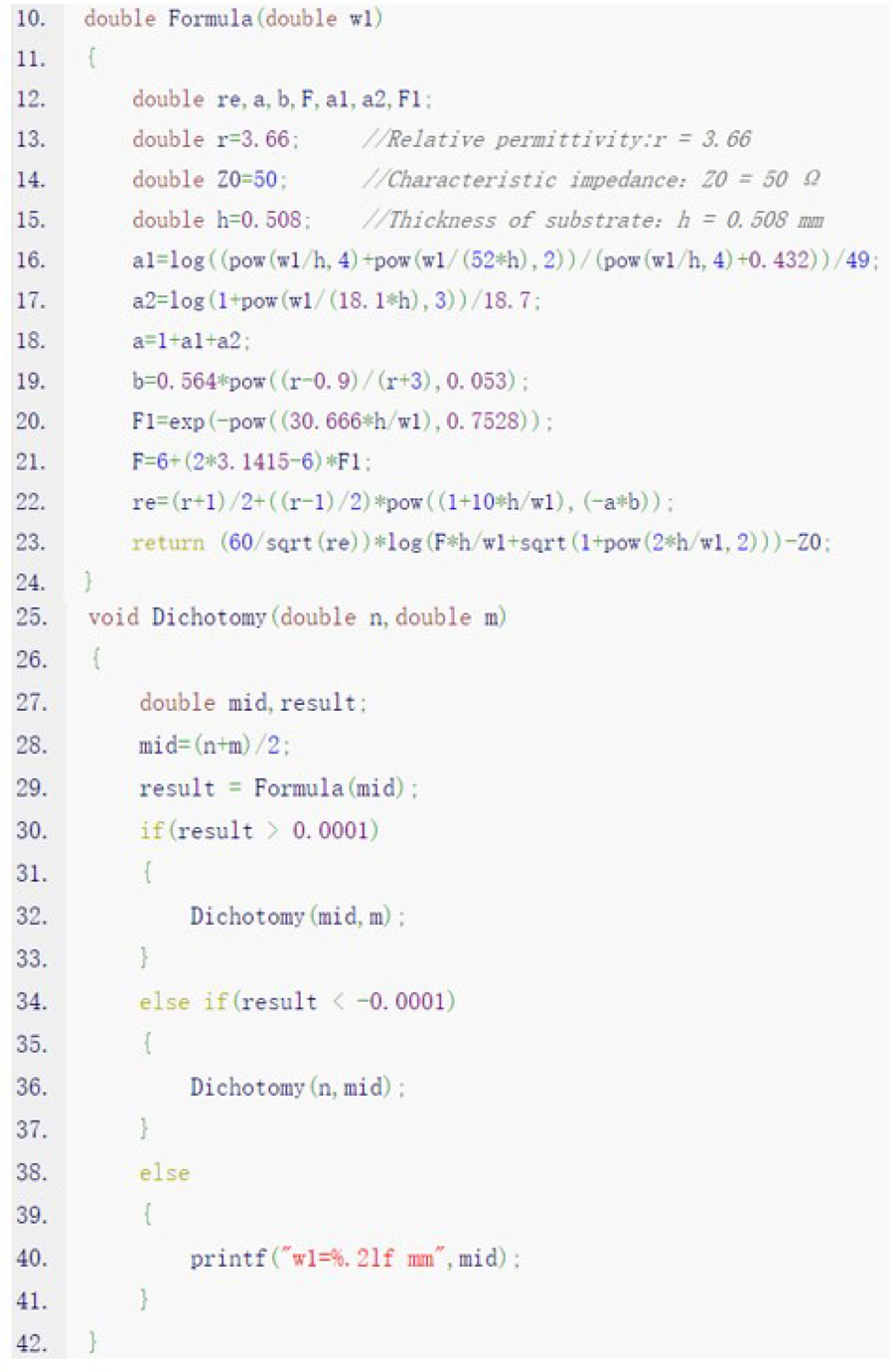
Figure 3: Relevant code for numerically solving microstrip width.
Figure 3 is the program code for numerically solving the microstrip width. After ensuring the relative dielectric constant of the substrate, the thickness of the substrate and the characteristic impedance of the microstrip, the width W of the microstrip with the characteristic impedance of 50 is 1.11 mm using the dichotomy method. The structure parameters W, d, w, t and g are defined by continuous simulation and optimization through High-Frequency Structure Simulator (HFSS) software. After adjusting the structural parameters, the resonant frequency interval of adjacent resonators is more than 250 MHz, which effectively reduces the mutual interference. Adjust the structural parameter d by HFSS software to reduce the coupling effect between adjacent resonators. Through continuous optimization and adjustment of the resonators, the structural parameters of the multi-state resonator tag for frequency sharing are finally determined. The specific values of the structural parameters are shown in Table 1.
Table 1: Structural parameters of the multi-state resonator (unit: mm)
| W | d | d | g | t | w |
| 1.07 | 0.2 | 2.2 | 0.9 | 1 | 0.5 |
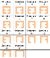
Table 2: Structural combinations of a resonator with various amounts of embedded OES
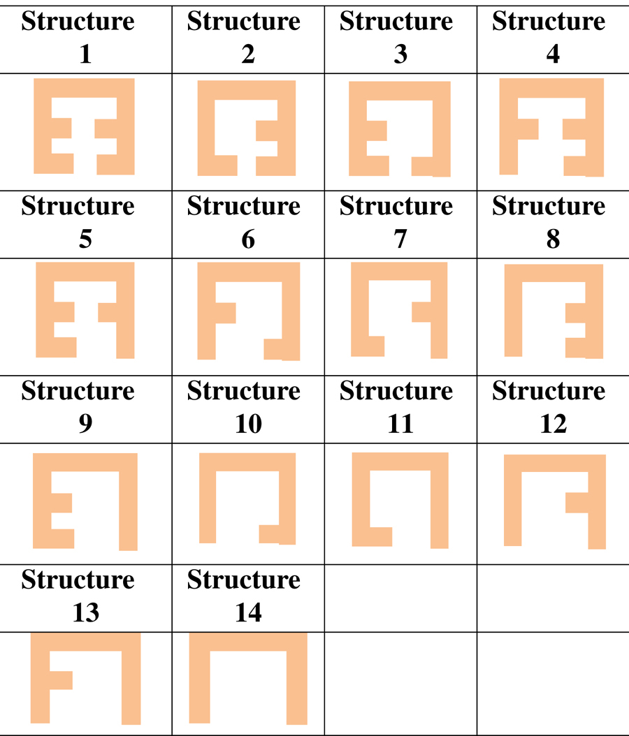
Different resonance frequencies can be obtained by various combinations of OES. When the maximum number of OES embedded in a resonator is 4, there are 14 structural combinations, as shown in Table 2. Among them, structures 2 and 3, structures 4 and 5, and structures 6 and 7, etc. are the same size and same resonance signature, respectively. Their equivalent circuits and resonance frequencies are the same as well. Therefore, there are only eight different resonance frequencies. But the adjacent resonance frequencies are quite close and may cause interference. Considering the above factors, for N=1 and M=4, the five structures of 1, 5, 8, 12 and 14 are selected in Table 2, thus five resonance frequencies are obtained correspondingly. N is the number of resonators of different sizes.
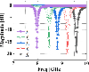
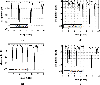
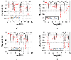
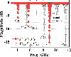
The simulation results of the resonator with N=1 and M=4 using an HFSS simulator are shown in Fig. 4, when w, g and t are 0.5, 0.9 and 1.0 mm, respectively. The curves with resonance frequencies f, f, f, f and fcorrespond to the resonators of structures 1, 5, 8, 12 and 14 in Table 2, respectively. The f-f resonant frequency point includes 7.97, 8.46, 8.81, 9.22 and 9.58 GHz, which has the maximum notch depth of 20 dB.
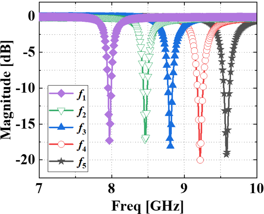
Figure 4: Response curve of the five-state single resonator structure (N=1, M=4).
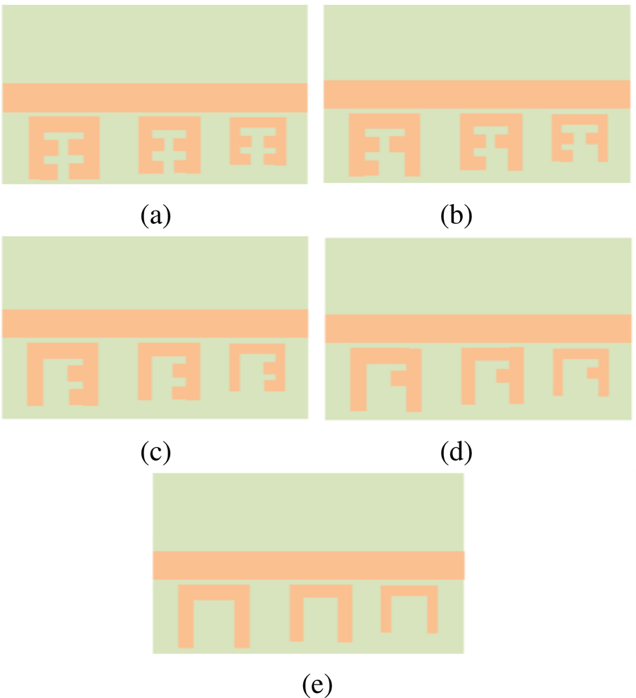
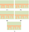
Figure 5: Schematic diagram of the structure (N=3, M=4): (a) fff; (b) fff; (c) fff; (d) fff; (e) fff.
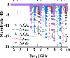
When N=3 and M=4, there are 15 resonance frequencies. The schematic diagrams of the structure are shown in Fig. 5. Where f is the resonance frequency of the N-th resonator, the number of the embedding OES is M. The resonance curves of simulation for the structure diagram of Fig. 5 with the parameter values of Table 1 are shown in Fig. 6. The intervals between the resonance frequencies corresponding to the spectral signature are within 250-490 MHz. The spectral signatures do not interfere with each other and the notch depth is between 11 dB to 18 dB. There is a weak interference with a notch depth of 3 dB at 9.91 GHz; however, for the resonance frequency f=9.72 GHz, the notch depth reaches 17 dB, the interference will not affect the encoding state. The set of 15 resonance frequencies in Fig. 6 is shown in Table 3, wherein the maximum and minimum intervals are 490 MHz and 250 MHz between adjacent resonancefrequencies.
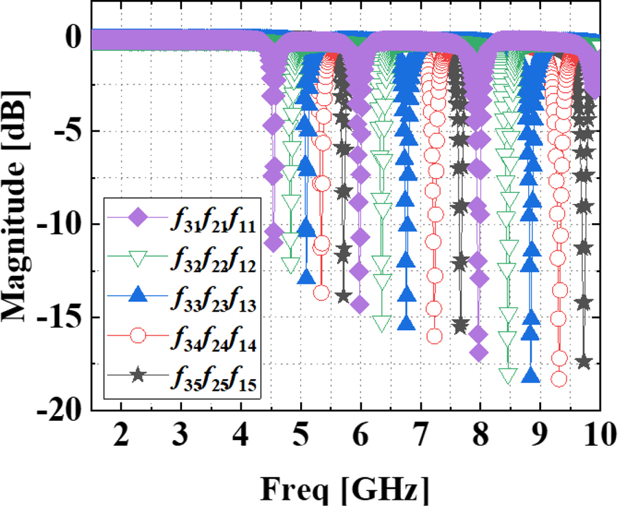
Figure 6: Resonance curves of the multi-state resonators (N=3, M=4).
Table 3: All resonance frequencies of the three multi-state resonators (unit: GHz)
| f | f | f | f | f |
| 7.97 | 8.46 | 8.84 | 9.31 | 9.72 |
| f | f | f | f | f |
| 5.98 | 6.35 | 6.76 | 7.23 | 7.66 |
| f | f | f | f | f |
| 4.54 | 4.83 | 5.09 | 5.34 | 5.71 |
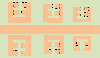
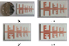
In order to improve the encoding capacity without increasing the dimension of the tag, using the sharing frequency method, a pair of the same size resonators is placed symmetrically on both sides of the coupled microstrip transmission line. The schematic diagram of the structure is shown in Fig. 7. When N=2, M=4, where N is a pair of the same size resonators, it can provide 15 different resonance frequencies. If a pair of the same size resonators is the resonator as shown in Fig. 5, it can be generated thus:
| (6) |
On the frequency axis, ff, ff, ff, ff and ff are all shown as curves with one resonance notch, and other data are shown as curves with two different resonance notches. However, in the above matrix (6), the data of the upper triangle and the lower triangle are repeated, which will cause data confusion in the tag identification of the item (for example, ff and ff have the same coding state on the spectrum). Therefore, the frequency combinations of the red or blue triangle box can be encoded. The total of 15 different resonance frequencies can be generated by using the sharing frequency method. For three pairs of resonators, there will be 15 codes, which is about 2. The combination method in mathematics can be used to calculate the number of different resonance frequencies.
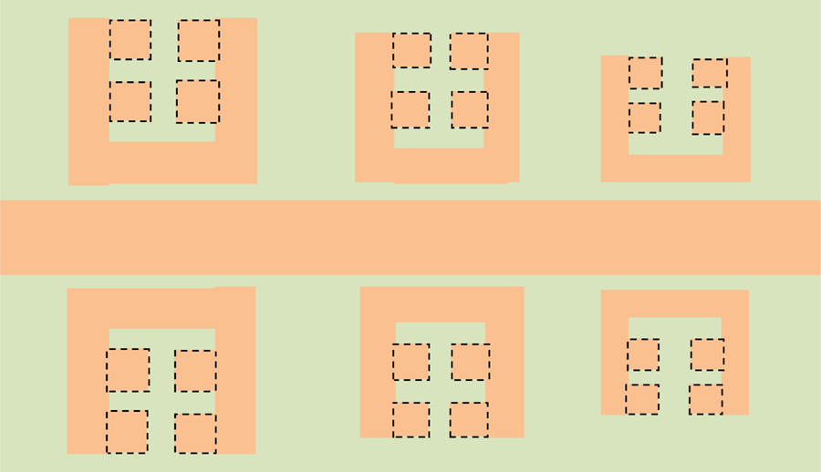
Figure 7: Schematic diagram of resonators of the same size in pairs (N=6).
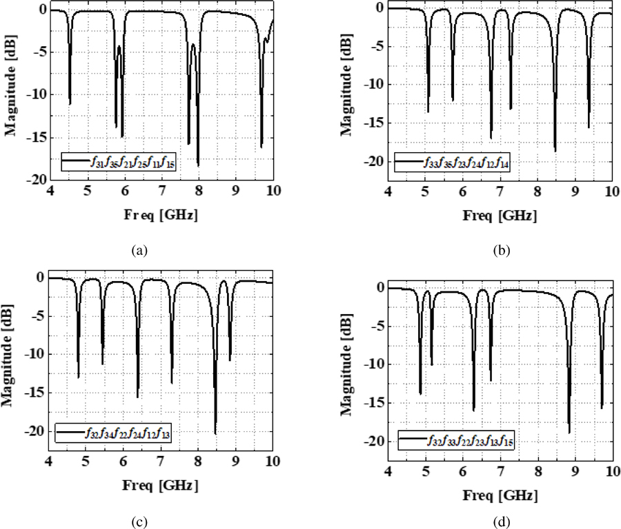
Figure 8: Resonance curves of four sharing frequency multi-state resonator tags: (a) ffffff; (b) ffffff; (c) ffffff; (d) ffffff.
Table 4: Resonance frequency of four sharing frequency multi-state resonator tags (unit: GHz)
| ffffff | f | f | f | f | f | f |
| Frequency Shift Compared With Table 3 | 4.52 | 5.76 | 5.93 | 7.72 | 7.97 | 9.68 |
| 0.02 | 0.05 | 0.06 | 0.06 | 0 | 0.04 | |
| ffffff | f | f | f | f | f | f |
| Frequency Shift Compared With Table 3 | 5.08 | 5.73 | 6.76 | 7.28 | 8.47 | 9.37 |
| 0.01 | 0.02 | 0 | 0.05 | 0.01 | 0.06 | |
| ffffff | f | f | f | f | f | f |
| Frequency Shift Compared With Table 3 | 4.80 | 5.45 | 6.39 | 7.30 | 8.46 | 8.85 |
| 0.03 | 0.11 | 0.04 | 0.07 | 0 | 0.01 | |
| ffffff | f | f | f | f | f | f |
| Frequency Shift Compared With Table 3 | 4.86 | 5.16 | 6.28 | 6.73 | 8.82 | 9.69 |
| 0.03 | 0.07 | 0.07 | 0.03 | 0.02 | 0.03 |
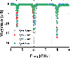
Figures 8 (a), (b), (c) and (d) are the resonance curves of tag coding ffffff, ffffff, ffffff and ff ffff based on the sharing frequency multi-state resonators. Table 4 shows the combinations of the resonance frequency encoding states of the four tags. Comparing the simulation results in Table 4 and Table 3, the maximum frequency offset is f in tag ffffff, which is 110 MHz. The maximum frequency offset does not exceed the minimum frequency interval of 250 MHz in Table 3, which will not cause error code.
IV. EXPERIMENT RESULTS
In accordance with the simulation results, several chipless tags with sharing frequency multi-state resonators are fabricated, named ffffff, ffffff, ffffff and ff ffff. Figure 9 is the photograph of the chipless tags with sharing frequency multi-state resonators. It can be seen that the tag is small in size, compared to the dime coin as a reference.
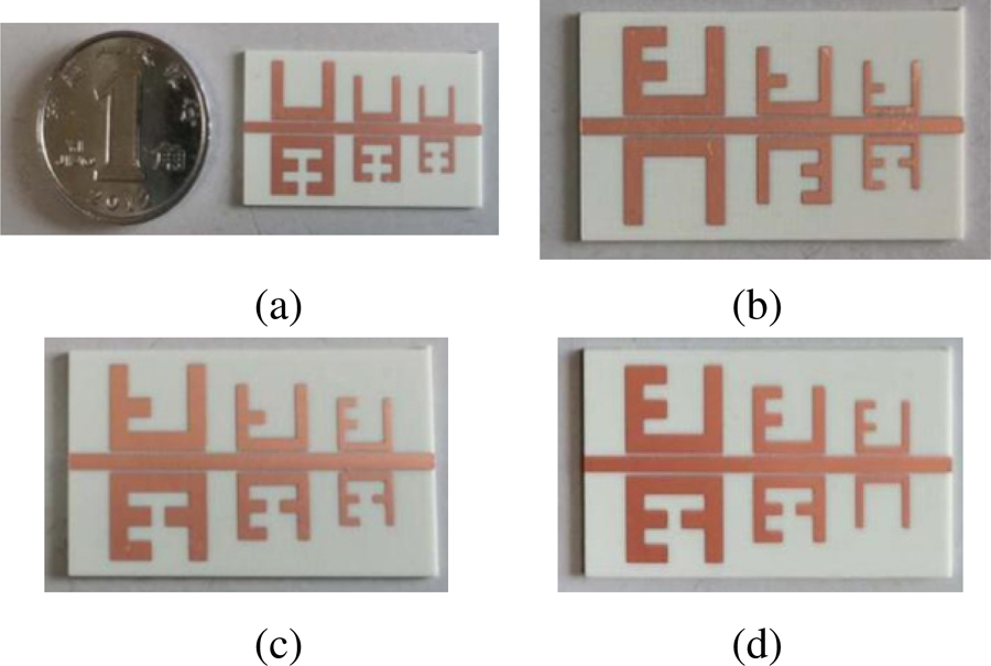
Figure 9: Photograph of chipless tags with sharing frequency multi-state resonators: (a) ffffff; (b) ffffff; (c) ffffff; (d) ffffff.
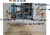
Figure 10 is the test system of a retransmitted chipless tag based on multi-state resonators. Ceyear vector network analyzer 3672D is used as an alternative to the UWB reader. The two ports of the network analyzer are connected to the two UWB disc monopole antennas, which are orthogonal to each other to improve the transceiver isolation of the reader. The chipless tag is also connected to two orthogonal UWB disc monopole antennas through two microwave connectors. In order to prevent the received signal and the transmitted signal of the tag from interfering with each other, the two-sided UWB antennas of the tag are also orthogonal to each other. The reader antennas and the tag antennas are fixed on the foam, and the distance between them is 30 cm.
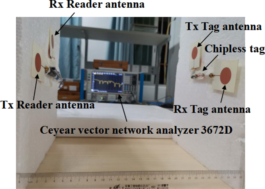
Figure 10: Test system.
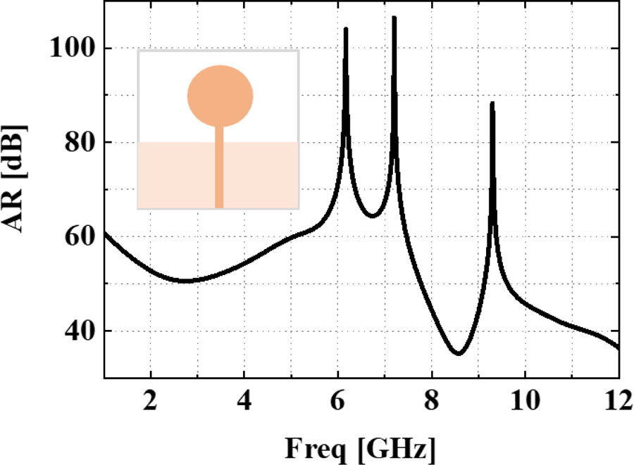
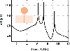
Figure 11: The AR curve of the UWB disc monopole antenna.
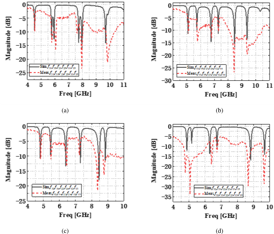
Figure 12: Simulation and measurement of resonance curves of four sharing frequency multi-state resonators tags: (a) ffffff; (b) ffffff; (c) ffffff; (d) ffffff.
The UWB disc monopole antenna is designed on RO4350 substrate with the structure of the literature [27], with the relative dielectric constant 3.66, the loss tangent 0.004, and the thickness of the substrate 1 mm. The axial ratio (AR) curve of the disc monopole antenna with a radius of 10 cm is shown in Fig. 11. The AR is much greater than 3 dB within the UWB frequency band, so the UWB disc monopole antenna has linearly polarized radiation. The polarization characteristics of the transmitting antenna of the reader and the receiving antenna of the tag are the same, but as they are orthogonal to the polarization characteristics of the transmitting antenna of the tag, polarization isolation will be formed. The transmitting antenna of the reader will not receive any signal from the tag. However, the receiving antenna of the reader can receive the signal from the tag. Similarly, the polarization characteristics of the receiving antenna of the reader and its transmitting antenna are orthogonal, so they will not affect each other. Just like the transceiver antennas of the reader are orthogonal to each other, the tag’s transceiver antennas are also orthogonal to each other. The configuration structure of the transceiver antenna of the reader and the tag’s transceiver antenna is shownin Fig. 10.
The UWB disc monopole antennas have the characteristics of omnidirectional radiation. In practical applications, the surrounding environment will definitely affect the chipless tag system. At this time, a UWB linearly polarized directional antenna is needed to reduce the impact of environmental factors on the tag system.
Figures 12 (a), (b), (c) and (d) show the characteristic results of simulation and measurement to the sharing frequency encoded tags. It can be seen from Fig. 12 that the simulation is consistent with the actual measurement. The maximum deviation of the resonance frequency points between the simulation and the measurement is 140 MHz, which is lower than the guard band of single resonance frequencies. The different amplitude between the simulation and measurement of each tag is mainly affected by the two antennas matching the tag and the performance of the UWB antenna. It will not affect the tag’s encoding state. The spectral signatures can correctly reflect the tag’sencoding data.
V. DISCUSSION
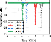
The mutual coupling between the resonance units can be reduced by increasing the spacing between the adjacent resonators. However, the resonance frequency shift may be generated. Figure 13 shows the resonance curve when the resonator spacing d is changed in Fig. 5 (a). When d increases from 1.5 mm to 4.6 mm, the resonator in the middle is affected by the resonators on both sides, and the resonance frequency is slightly shifted. The resonators on both sides are less affected, and the resonance frequency points are almost unchanged. The mutual coupling effect between the resonators can be reduced by adjusting the resonatorspacing d.
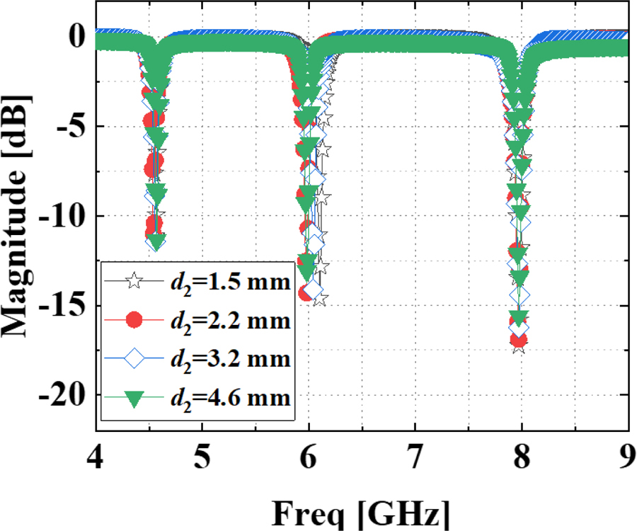
Figure 13: Resonance curves of the resonator when spacing d is changed from 1.0 mm to 4.6 mm.
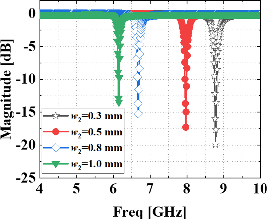
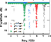
Figure 14: Resonance curves of the structure 1 when w is changed from 0.3 mm to 1.0 mm.
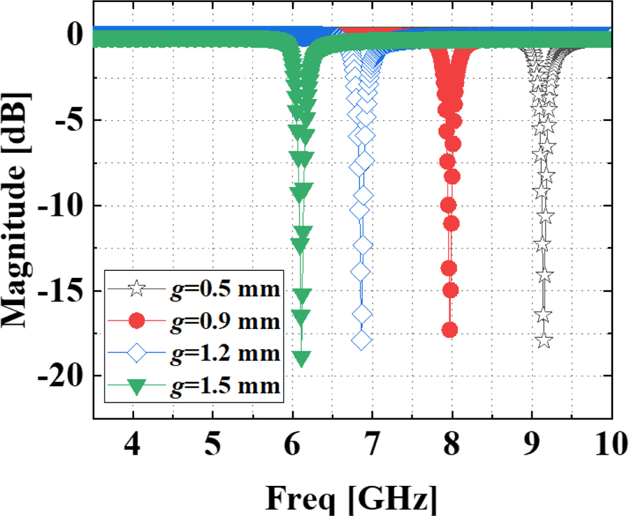
Figure 15: Resonance curves of the structure 1 when g is changed from 0.5 mm to 1.5 mm.
Figures 14 and 15 are the simulated resonance curves of Structure 1 in Table 2 when the width w and length g of the OES are changed, respectively. As w becomes wider and g becomes longer, the resonance frequency becomes smaller, while the bandwidth occupied by the resonator is almost unchanged. As w becomes wider, the notch depth of the resonance frequency becomes shallower.
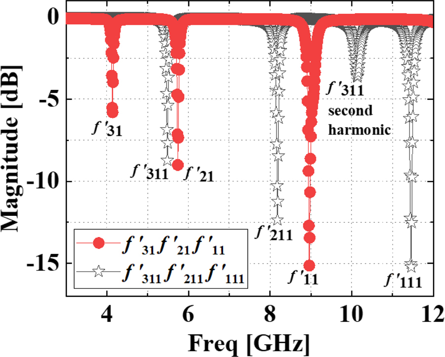
Figure 16: Operating bandwidth of sharing frequency multi-state resonator tags where N=3, M=10.
Table 5: Comparison of different types of retransmitted chipless tags
| Resonator Type | Operating Frequency Band (GHz) | Capacity (bits/cm) | Encoding Capacity (bits/cm/GHz) | Tag Area (mm) | Substrate |
| Spiral [3] | 3-7 | 0.61 | 0.15 | 8865 | Taconic TLX-0 |
| Spiral [19] | 5-11 | 0.33 | 0.06 | 10864 | Taconic TF-290 |
| Open Stubs [20] | 4-9 | 0.24 | 0.05 | 11060 | Rogers 4003C |
| Open Loop [22] | 3-6 | 0.25 | 0.08 | 8538 | Rogers 5880 |
| Purline Resonators [23] | 2.4-4.2 | 0.09 | 0.05 | 15060 | C-MET/LK4.3 |
| Cascades E-shaped [24] | 3.3-4.3 | 0.05 | 0.05 | 160100 | C-MET/LK4.3 |
| Multi-state Resonators (N=6, M=4) (Proposed) | 4.8-9.7 | 0.87 | 0.18 | 4630 | Rogers 4350 |
For a tag of N=3 and M=10, a single resonator has 11 different resonance frequencies, and 3 resonators of different sizes have a total of 33 different resonance frequencies. In order that adjacent resonance frequencies do not affect each other, the structural parameters w, g and t are adjusted to 0.2 mm, 0.6 mm and 0.4 mm, respectively through simulation. According to the simulation results, the three resonators’ working bandwidths are shown as f-f, f-f, and f-f in Table 4. As long as the resonator structures of Figs. 5 (a) and 5 (e) are simulated, the operating bandwidths of the tags can be determined, and the simulation results are shown in Fig. 16. Where f’ is the resonance frequency of the N-th resonator, the number of the embedding OES is M. The operating bandwidths of the three resonators f’-f’, f’-f’, and f’-f’ of M=10 are 4.14-5.18, 5.74-8.18 and 8.96-11.46 GHz, respectively. The notch depth is between 5.8 and 15.23 dB. However, the second harmonic of f’ appears at 10.14 GHz in Fig. 16. The notch depth of the 2nd harmonic is 3.65 dB. This interference of the 2nd harmonic on the spectrum signature can be removed by signal processing and certain algorithms. For N=3 and M=10, the total of 33 resonant frequency signatures can generate 11 codes, which is about 2. When the number of resonators is six, the encoding state of the chipless tag based on the sharing frequency multi-state resonators is 66, which isabout 2.
Table 5 shows the comparisons among different retransmitted chipless tags, including the aspects of bandwidth (GHz), capacity (bits/cm), encoding capacity (bits/cm/GHz), tag area (mm) and substrate. It can be seen that the proposed chipless tags show the most promising properties as the retransmitted chipless tag among all the listed results. Although the spiral resonator chipless tag has high capacity, this tag is limited by its large area. The open loop resonator has low encoding capacity of 0.08 bits/cm/GHz and a large area compared with this work. The open stubs, purline and cascades E-shaped resonators also have large tag areas and low encoding capacity. In summary, the retransmitted chipless tag of the OES multi-state resonator that we propose in this paper has a small area and large encoding capacity.
VI. CONCLUSION
This paper proposes a chipless tag for sharing frequency multi-state resonators based on the retransmission structure. This work demonstrates a frequency sharing method based on the retransmitted chipless tag. U-shaped microstrip resonators are used to embed some OES lines to implement the frequency sharing, which achieves the purpose of saving spectrum and improving spectrum utilization. The number of different resonance frequencies of the sharing frequency can be calculated using a combination in mathematics. The sharing frequency method aims to realize small size tags with a large encoding capacity. This chipless tag includes U-shaped microstrip resonators, the OES line and a 50 microstrip transmission line. The sharing frequency multi-state resonator chipless tag was fabricated on RO4350 substrate. The operating frequency band of 4.8-9.7 GHz is designed where N=6, M=4, a pair of the same size resonators is placed symmetrically on both sides of the coupled microstrip transmission line. This chipless tag with an area of 46 30 mm can generate about 2 encoding states. The capacity is 0.87 bits/cm. The encoding capacity is 0.18 bits/cm/GHz. The communication distance is 30 cm. Each resonator has only two states in the traditional retransmitted chipless tag. Six resonators can only realize 2 encoding states, whose encoding capacity is less than the multi-state resonators.
Using HFSS software, simulation shows that the intervals between the resonance frequencies corresponding to the spectral signature are within 250-490 MHz, and the spectral signatures do not interfere with each other. The simulation and measurement are in good agreement. This paper increases the number of embedded OES in the U-shaped microstrip resonator to increase the coding capacity. The sharing frequency method is used to improve the spectrum utilization rate. In the future, it is proposed to further increase the coding capacity and solve the key problem of anti-collision of the chipless tag. The cost of this chipless tag is low which means it can be widely used in logistics, supermarkets and other fields to replace the barcode.
ACKNOWLEDGMENT
This work was supported by the Fujian Natural Science Foundation Project (2022J01823) and the National Fund training project of Jimei University (ZP2020039).
REFERENCES
[1] U. Kaiser and W. Steinhagen, “A low-power transponder IC for highperformance identification systems,” IEEE Journal of Solid-State Circuits, vol. 30, no. 3, pp. 306-310, Mar. 1995.
[2] S. Preradovic and N. C. Karmakar, “Chipless RFID: bar code of the future,” IEEE Microwave Magazine, vol. 11, no. 7, pp. 87-97, Dec. 2010.
[3] S. Preradovic, I. Balbin, N. C. Karmakar, and G. F. Swiegers, “Multiresonator-based chipless RFID system for low-cost item tracking,” IEEE Transactions on Microwave Theory and Techniques, vol. 57, no. 5, pp. 1411-1419, May 2009.
[4] C. Herrojo, J. Mata-Contreras, F. Paredes, A. Núñez, E. Ramon, and F. Martín, “Near-field chipless-RFID system with erasable/programmable 40-bit tags inkjet printed on paper substrates,” IEEE Microwave and Wireless Components Letters, vol. 28, no. 3, pp. 272-274, Mar. 2018.
[5] A. Ali, S. I. Jafri, A. Habib, Y. Amin, and H. Tenhunen, “RFID humidity sensor tag for low-cost applications,” Applied Computational Electromagnetics Society (ACES) Journal, vol. 32, no. 12, pp. 1083-1088, May 2017.
[6] A. Chamarti and K. Varahramyan, “Transmission delay line based ID generation circuit for RFID applications,” IEEE Microwave and Wireless Components Letters, vol. 16, no. 11, pp. 588-590, Nov. 2006.
[7] A. Stelzer, S. Scheiblhofer, S. Schuster, and M. Brandl, “Multi reader/Multi-tag SAW RFID systems combining tagging, sensing, and ranging for industrial applications,” IEEE International Frequency Control Symposium, Honolulu, HI, USA, pp. 263-272, May 2008.
[8] B. Shao, Q. Chen, Y. Amin, S. M. David, R. Liu, and L. Zheng, “An ultra-low-cost RFID tag with 1.67 Gbps data rate by ink-jet printing on paper substrate,” IEEE Asian Solid-State Circuits Conference, Beijing, China, pp. 1-4, Nov. 2010.
[9] C. S. Hartmann, “A global SAW ID tag with large data capacity,” IEEE Ultrasonics Symposium, Munich, Germany, vol. 1, pp. 65-69, Oct. 2002.
[10] J. Liu and J. Yao, “Wireless RF identification system based on SAW,” IEEE Transactions on Industrial Electronics, vol. 55, no. 2, pp. 958-961, Feb. 2008.
[11] S. Haermae, V. P. Plessky, C. S. Hartmann, and W. Steichen, “Z-path SAW RFID tag,” IEEE Transactions on Ultrasonics Ferroelectrics and Frequency Control, vol. 55, no. 1, pp. 208-213, Jan. 2008.
[12] V. P. Plessky and L. M. Reindl, “Review on SAW RFID tags,” IEEE Transactions on Ultrasonics Ferroelectrics and Frequency Control, vol. 57, no. 3, pp. 654-668, Mar. 2010.
[13] M. Polivka, J. Havlicek, M. Svanda, and J. Machac, “Improvement in robustness and recognizability of RCS response of U-shaped strip-based chipless RFID tags,” IEEE Antennas and Wireless Propagation Letters, vol. 15, pp. 2000-2003, Apr.2016.
[14] M. Svanda, M. Polivka, J. Havlicek, and J. Machac, “Chipless RFID tag with an improved magnitude and robustness of RCS response,” Microwave and Optical Technology Letters, vol. 59, no. 2, pp. 488-492, Feb. 2017.
[15] M. Svanda, J. Havlicek, J. Machac, and J. Polivka, “Polarisation independent chipless RFID tag based on circular arrangement of dual-spiral capacitively-loaded dipoles with robust RCS response,” IET Microwaves Antennas and Propagation, vol. 12, no. 14, pp. 2167-2171, Nov. 2018.
[16] N. Chen, Y. Shen, G. Dong, and S. Hu, “Compact scalable modeling of chipless RFID tag based on high-impedance surface,” IEEE Transactions on Electron Devices, vol. 66, no. 1, pp. 200-206, Jan. 2019.
[17] G. Q. Dong, Y. Z. Shen, H. F. Meng, N. Chen, and W. B. Dou. “Printable chipless tag and dual-CP reader for internet of things,” Applied Computational Electromagnetics Society (ACES) Journal, vol. 33, no. 5, pp. 494-498, May 2018.
[18] S. Preradovic and N. C. Karmakar, “Design of fully printable planar chipless RFID transponder with 35-bit data capacity,” European Microwave Conference (EuMC), Rome, Italy, pp. 13-16, 2009.
[19] S. Preradovic, S. Roy and N. Karmakar, “Fully printable multi-bit chipless RFID transponder on flexible laminate,” Asia Pacific Microwave Conference, Singapore, pp. 2371-2374, Sep. 2009.
[20] M. A. Ashraf, Y. A. Alshoudokhi, H. M. Behairy, M. R. Alshareef, S. A. Alshebeilim, K. Issa, and H. Fathallah, “Design and analysis of multi-resonators loaded broadband antipodal tapered slot antenna for chipless RFID applications,” IEEE Access, vol. 5, pp. 25798-25807, Oct. 2017.
[21] Y. F. Weng, S. W. Cheung, T. I. Yuk, and L. Liu, “Design of chipless UWB RFID system using a CPW multi-resonator,” IEEE Antennas and Propagation Magazine, vol. 55, no. 1, pp. 13-31, Feb. 2013.
[22] V. Sharma and M. Hashmi, “Chipless RFID tag based on open-loop resonator,” IEEE Asia Pacific Microwave Conference (APMC), Kuala Lumpur, Malaysia, pp. 543-546, Nov. 2017.
[23] M. Sumi, C. M. Nijas, R. Dinesh, S. Mridula, and P. Mohanan, “Spectral signature-encoded chipless RFID tag with planar multiresonators,” Journal of Electromagnetic Waves and Applications, vol. 28, no. 18, pp. 2266-2275, Dec. 2014.
[24] M. Sumi, R. Dinesh, C. M. Nijas, S. Mridula, and P. Mohanan, “High bit encoding chipless RFID tag using multiple E shaped microstrip resonators,” Progress in Electromagnetics Research B, vol. 61, no. 2014, pp. 185-196, Nov. 2014.
[25] E. O. Hammerstad and O. Jensen, “Accurate models for microstrip computer-aided design,” International Microwave Symposium Digest IEEE, pp. 407-409, May 1980.
[26] E. Q. Hammerstard, “Equations for microstrip circuit design.” IEEE European Microwave Conference, Hamburg, Germany, pp. 268-272, Sept. 1975.
[27] J. X. Liang, C. C. Chiau, X. D. Chen, and C. G. Parini, “Study of a printed circular disc monopole antenna for UWB systems,” IEEE Transactions on Antennas and Propagation, vol. 53, no. 11, pp. 3500-3504, Nov. 2005.
BIOGRAPHIES

Huang Nengyu received her bachelor’s degree from the University of South China in 2019. She is currently working on her M.S. degree in Traffic and Transportation Engineering at Jimei University, Fujian Province, China. Her research interest is radio frequency identification (RFID).

Ma Zhonghua was born in Gansu, Republic of China, in 1973. He received his M.S. degree in Information Engineering and Communication and Information Systems in 2004 and his Ph.D degree in Microelectronics in 2018, both from Lanzhou University. His present research interests include antenna techniques, RF circuit design and RFID systems. His current research concerns the field of chipless RFID sensors.
ACES JOURNAL, Vol. 38, No. 4, 251–262
doi: 10.13052/2023.ACES.J.380404
© 2023 River Publishers