Research on the Prediction Method of Conducted Interference in Flyback Converters based on the High-frequency Transformer Model
Mengxia Zhou2, Bin Cheng2, Jianben Liu1, Yakang Pei2, Ruining Yao2, Yan Liu1, and Feng Li2*
1State Key Laboratory of Power Grid Environmental Protection
China Electric Power Research Institute, Wuhan 430074, China
liujianben@epri.sgcc.com, 1029358940@qq.com
2School of Electrical and Automation Engineering
Nanjing Normal University, Nanjing 210023, China
61239@njnu.edu.cn, 211846067@njnu.edu.cn, eaepyk@nnu.edu.cn,
6598691@qq.com, 61238@njnu.edu.cn
*Corresponding author
Submitted On: May 8, 2023; Accepted On: February 4, 2024
ABSTRACT
Conducted electromagnetic interference (EMI) has always been a challenge for designers of switched-mode power supplies. Flyback converters are used in various applications. However, as the switching frequency of these converters increases, the issue of electromagnetic interference becomes progressively more severe. In light of this, this paper presents a predictive method for conducted interference in flyback converters, based on a high-frequency transformer model. A high-frequency transformer model topology is proposed, integrating traditional inductance models with a three-capacitor model. Subsequently, a self-organizing migrating algorithm (SOMA) is employed for the extraction of parameters from the high-frequency transformer model, and a high-frequency model is established for a transformer. Finally, the high-frequency model is applied to the prediction of conducted interference in flyback converters. The results demonstrate that the proposed predictive method can effectively forecast the actual conducted interference, thereby providing a reference for suppression of conducted electromagnetic interference.
Index Terms: Conducted interference, high-frequency model, interference prediction, self-organizing migrating algorithm (SOMA), transformer.
I. INTRODUCTION
With the continuous development of power electronics technology, the issue of electromagnetic interference (EMI) in flyback converters is becoming increasingly severe. Additionally, transformers in flyback converters have a significant impact on EMI. First, the flyback converter transformer occupies a large volume and weight, and its parameter characteristics have a considerable impact on the performance of the flyback converter and EMI characteristics. In addition, the transformer is mostly designed independently, and their high-frequency characteristics are affected by factors such as design, production process, and installation location [1]. Therefore, a reasonable study and design of transformer can ensure a better parameter fit between components, which can significantly improve the EMI problems of flyback converters.
There have been many studies related to the low-frequency characteristics of transformers, and most of them are relatively mature [2–6]. Although there has been some research into the high-frequency characteristics of transformers, the proposed transformer models were relatively complex in computation [7–11].
In the study of disturbances in flyback converters, Ferber et al. used MATLAB to model the flyback converters, but their flyback converters model is relatively simple and has no feedback circuit, so it is not good at predicting the conducted disturbance waveform of the switching power supply in actual operation [12]. Chen and Liu investigated methods to reduce the conducted interference in flyback converters. The computational model for the equivalent common-mode capacitance in transformers was established. However, the comprehensive high-frequency model for transformers model has not yet been established [13].
In Section II, a high-frequency transformer topology combining the conventional inductor model and the three-capacitor model is proposed. The equivalent circuit topology for each parameter in the high-frequency transformer model is obtained in Section III, and the parameters are extracted using self-organizing migrating algorithm (SOMA). In Section IV, a transformer is selected for high-frequency modeling. In Section V, the developed high-frequency model of the transformer is applied to the conducted disturbance prediction of the flyback converter, and the modeling method of the high-frequency model of the transformer is verified.
II. HIGH-FREQUENCY TRANSFORMER MODEL
A. Inductance characteristics
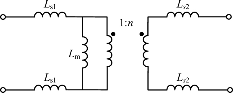
At low frequencies, the primary and secondary sides of the transformer are mainly coupled magnetically, and the primary and secondary inductors are linked by mutual inductance. However, this model can only be used to reflect the principle and basic topology of the transformer and ignores the transformer losses, so it is not suitable for circuit simulation. The model considered in terms of the magnetic field inside the transformer is shown in Fig. 1, where the excitation branch corresponds to the excitation inductance L and the leakage path corresponds to the leakage inductances L and L.
Figure 1: Transformer excitation inductance and leakage inductance model.
Considering that transformers are inevitably accompanied by iron and copper losses in operation, the effect of adding resistances to equate transformer losses on the basis of Fig. 1 is shown in Fig. 2. As can be seen from Fig. 2, the parallel resistance R of the excitation branch of the inductance model is equivalent to the iron loss of the transformer; the series resistances R and R of the leakage branch are equivalent to the copper losses of the primary and secondary of the transformer, respectively.
Figure 2: Transformer low frequency loss inductance equivalent model.
Although some improvements have been made to the equivalent model, it still only represents the relevant characteristics of the transformer in the lower frequency range. Because the model does not reflect the effect of transformer distributed parameters at high frequencies, it is not suitable for studying the conducted disturbances in switched-mode power supplies. Therefore, the distributed parameters of the transformer at high frequencies will be analyzed in order to facilitate the subsequent study of conductor disturbances.
B. Capacitance characteristics
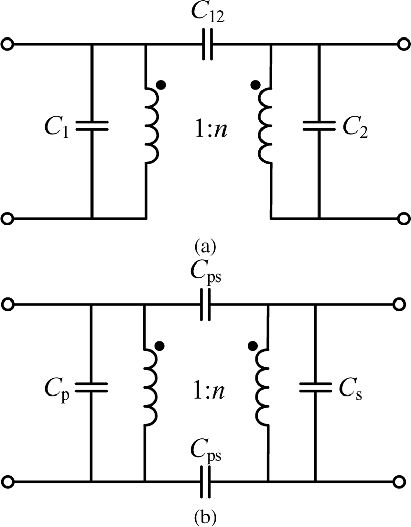
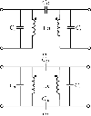
The distributed capacitance of the transformer is generally considered not to change with frequency [14]. The transformer triple capacitance model is shown in Fig. 3 (a) where C represents the equivalent self-capacitance of the primary side of the transformer, C is the equivalent self-capacitance of the secondary side, and C is the capacitance between the primary and secondary sides. However, in order to facilitate the interference path analysis of conducted disturbances, the equivalent model of the transformer is improved. The improved transformer distributed capacitance model, shown in Fig. 3 (b), adds a capacitor below the transformer, making the model more convenient for the analysis of conducted disturbances in flyback converters.
Figure 3: Transformer (a) three-capacitor model and (b) four-capacitor model.
C. High-frequency equivalent model
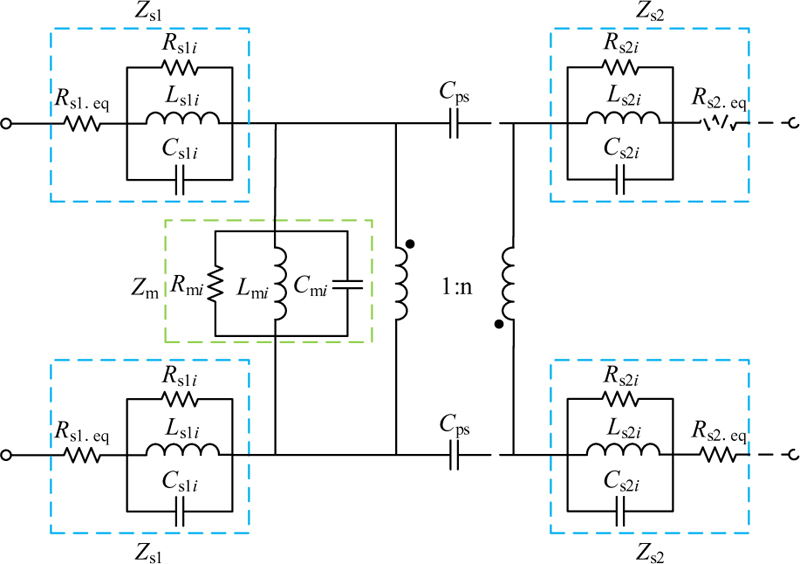
Combining the low-frequency loss inductance model of the transformer with the four-capacitance equivalent model, a high-frequency equivalent model of the transformer is obtained, as shown in Fig. 4. Z and Z are the combined equivalent impedances of the copper loss and leakage inductance of the first and second sides of the transformer, respectively. Z is the combined equivalent impedance of the core iron loss R, the excitation inductance L, and the primary side winding self-variable capacitance C. C is the secondary side winding self-capacitance and C is a secondary side capacitance between the windings.
Figure 4: Transformer high-frequency equivalent model.
III. PARAMETER EXTRACTION FOR THE HIGH-FREQUENCY TRANSFORMER MODEL
In parameter extraction for transformers in this paper, SOMA is used to process the transformer-related impedance data to obtain the RLC parameters in the high-frequency model [15]. The high-frequency modeling of transformers is accomplished by using SOMA, which essentially processes the impedance measurement data of transformers in order to solve for the relevant RLC parameters in their equivalent circuits in order to obtain the optimal solutions for the above parameters. The steps in SOMA for processing transformer impedance data are as follows [16]:
Step 1: Impedance extraction for high-frequency model parameters of transformers.
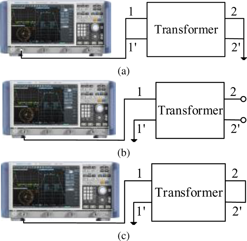
Figure 5: Measurement methods for transformer high-frequency model parameters: (a) inter-winding impedance, (b) excitation impedance, and (c) leakage inductance impedance.
In the process of measuring the inter-winding capacitance of a transformer, its primary and secondary sides are short-circuited, respectively. Then, using a vector network analyzer (VNA), the impedance curve is measured, as shown in Fig. 5 (a). To measure the transformer’s excitation impedance, Z, the secondary side of the transformer is left open-circuited. The impedance of the primary side is then measured with a VNA, as depicted in Fig. 5 (b). For measuring the transformer’s leakage inductance impedances, Z and Z, the secondary side is short-circuited, and the primary side impedance is measured using a VNA, as illustrated in Fig. 5 (c).
Step 2: Equivalent circuit topology and expressions.
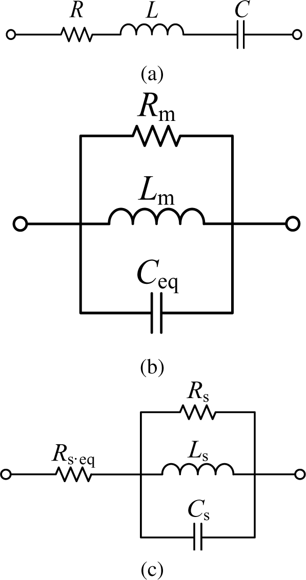
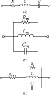
After obtaining the measured inter-winding impedance of the transformer, for ease of calculation, the inter-winding capacitance in the transformer’s high-frequency model is considered in parallel. The high-frequency model of the capacitance is used for equivalence, with the equivalent circuit topology as shown in Fig. 6 (a). Hence, the expression for inter-winding impedance is:
| (1) |
The transformer’s excitation impedance is significantly larger than the leakage magnetic impedance Z, thus the effect of leakage magnetic impedance on excitation impedance is neglected. The equivalent circuit topology for excitation impedance is shown in Fig. 6 (b). The derived expression for excitation impedance at this stage is:
| (2) |
The impedance measured represents the total leakage inductance of the transformer’s primary and secondary sides. For ease of analysis, the leakage inductances of the primary and secondary sides are distributed according to the square of the transformation ratio. For the transformer’s leakage inductance impedances Z and Z, considering the frequency-dependent effect of the leakage inductance, R and R were modified to R and R, respectively. The right-side inductors L and L use a high-frequency equivalent model. The final high-frequency equivalent model for leakage inductance is shown in Fig. 6 (c), with its impedance expression as follows:
| (3) |
Figure 6: Equivalent circuit topology of parameters
Normalization results in the following high-frequency model of the transformer. The high-frequency models for magnetizing and leakage inductance are composed of ‘i’ serially connected modules, where ‘i’ is the number of segments used during impedance measurement.
Figure 7: Transformed high-frequency equivalent model of the transformer.
Step 3: Transformation of the optimal parameter problem.
The impedance expression obtained from the transformer equivalent circuit topology is transformed into an expression for the impedance amplitude Z, and then Z is used as the original function of the RLC parameters to be optimized, and the measured frequency-dependent impedance data Z is the sample. Let the expression of the impedance amplitude Z of the transformer-equivalent circuit model be:
| (4) |
where D represents the number of circuit parameters, ƒ is the independent variable (frequency), Z is the dependent variable (impedance), and x,x,x,…,xare the parameters to be determined, which in this paper correspond to the RLC parameters of the impedance equivalent model.
The optimization criterion function can be established based on the least squares sum of the residuals of the system model, as follows:
| (5) |
where (f) represents the measured impedance magnitude values of the transformer and (f)’ is the calculated impedance magnitude value of the impedance equivalent circuit. When the variable Q is minimized, the corresponding RLC parameters are considered as the optimal parameters.
Step 4: Define the parameters.
Population size, N; Step size, Step; Path length, PathLength; Perturbation, PRT; and Migration loop count, ML.
Step 5: Initialization parameters.
Randomly generated for the initial population
| (6) |
where N is the population size, x(0) refers to the mth individual of the 0th generation in the total, x(0) refers to the nth gene of the mth individual of the 0th generation, andandare the minimum and maximum values of the nth gene of the mth individual, respectively. The rand function generates pseudo-random numbers uniformly distributed between 0 and 1.
Step 6: Migration process.
The migration action formula is:
| (7) |
where is the value of u individuals after ML+1 migration; is the position of u individuals at the beginning of migration; is the leader position at the time of migration; v is the dimension; t(0, PathLength), t is the interval length in steps, and the maximum is taken as PathLength; PRTVector is a vector that depends on PRT; if the random number at (0, 1) is smaller than PRT, then PRTVector is set to 1, otherwise it is set to 0.
Step 7: End of algorithm.
The termination criteria are met when the error between particles reaches the set value of MinDiv, or when the number of migration loops reaches the ML. The end condition is assessed to determine if it has been achieved. If the termination criteria are not met, the process returns to Step 6. If the termination criteria are met, the process concludes. As a result, the optimal values of RLC parameters in each impedance formula are obtained.
IV. TRANSFORMER HIGH-FREQUENCY MODEL TEST VERIFICATION
In this paper, the high-frequency characteristics of the transformer in the flyback converter prototype are modeled. The core material is ferrite, the model is EC28/34, the winding method is sandwich winding, and the ratio of primary to secondary turns is 37:3. In the modeling of the transformer, the impedance curve is also divided into frequency bands. In this way, it is possible to process the measured impedance data with SOMA and obtain highly accurate RLC values, even without using a professional workstation computer.
The capacitive characteristics of transformers indicate that the distributed capacitance of transformers does not vary with frequency. Therefore, when modeling the inter-winding capacitance, only the impedance curve between transformer windings in the frequency range of 1-50 MHz is measured using VNA for easy processing and saving computational resources. In the process of measuring the inter-winding capacitance of a transformer, its primary and secondary sides are short-circuited, respectively. The impedance data is fitted using SOMA and (1) to obtain the RLC parameter in (1). The final obtained parameters are shown in Table 1.
Table 1: RLC values for the high-frequency model of inter-winding impedance
| R | L | C |
| 4.13 | 0.20 µH | 118.96 pF |
In modeling the high-frequency characteristics of the excitation impedance, the secondary side of the transformer is open-circuited, and then the excitation impedance curve in the frequency range of 9 kHz-200 MHz on the primary side of the transformer is measured using a VNA. Then the impedance data are divided into three frequency bands based on the number of valleys in the impedance curve obtained from the measurements. Finally, SOMA and (2) are used to fit the impedance data, and then the RLC parameters in the excitation impedance high-frequency model are obtained. The RLC parameters of the excitation impedance high-frequency model are shown in Table 2.
Table 2: RLC values for the high-frequency model of excitation impedance
| i = 1(150 kHz-96 MHz) | i = 2(96-186 MHz) | i = 3(186-200 MHz) | |
|---|---|---|---|
| R | 64.14 k | 910.16 | 346.93 |
| L | 0.33 mH | 0.13 µH | 15.02 nH |
| C | 9.43 pF | 13.88 pF | 40.96 pF |
The leakage inductance of the transformer was measured by shorting the secondary side of the transformer and then measuring the impedance data and waveforms in the frequency range of 9 kHz-200 MHz on the primary side of the transformer using a VNA. Then the impedance data was divided into three frequency bands according to the characteristics of the leakage inductance waveform. Finally, the excitation impedance data are processed using SOMA and (3) to obtain the RLC parameters, as shown in Table 3, where R is 10 n, which is obtained by connecting the resistors of the three frequency bands in series.
Table 3: RLC values for the high-frequency leakage inductance model
| i = 1(150 kHz-96 MHz) | i = 2(96-186 MHz) | i = 3(186-200 MHz) | |
|---|---|---|---|
| R | 7.92 k | 871.03 | 373.64 |
| L | 4.54 µH | 0.12 µH | 14.36 nH |
| C | 8.84 pF | 14.88 pF | 42.69 pF |
The transformation of primary and secondary impedances in a transformer is governed by the following relationship:
| (8) |
where Z is the primary impedance of the transformer, Z is the secondary impedance, and n is the transformation ratio of the transformer.
For the high-frequency equivalent circuit topology of the leakage inductance, there is:
| (9) |
where Z represents the impedance values before applying the transformer’s transformation ratio.
Using (8) and (9), the transformed values of the primary and secondary leakage impedances of the transformer can be obtained, as shown in Table 4 [17]. Among them, R and R are 2.50 n and 16.40 p, respectively.
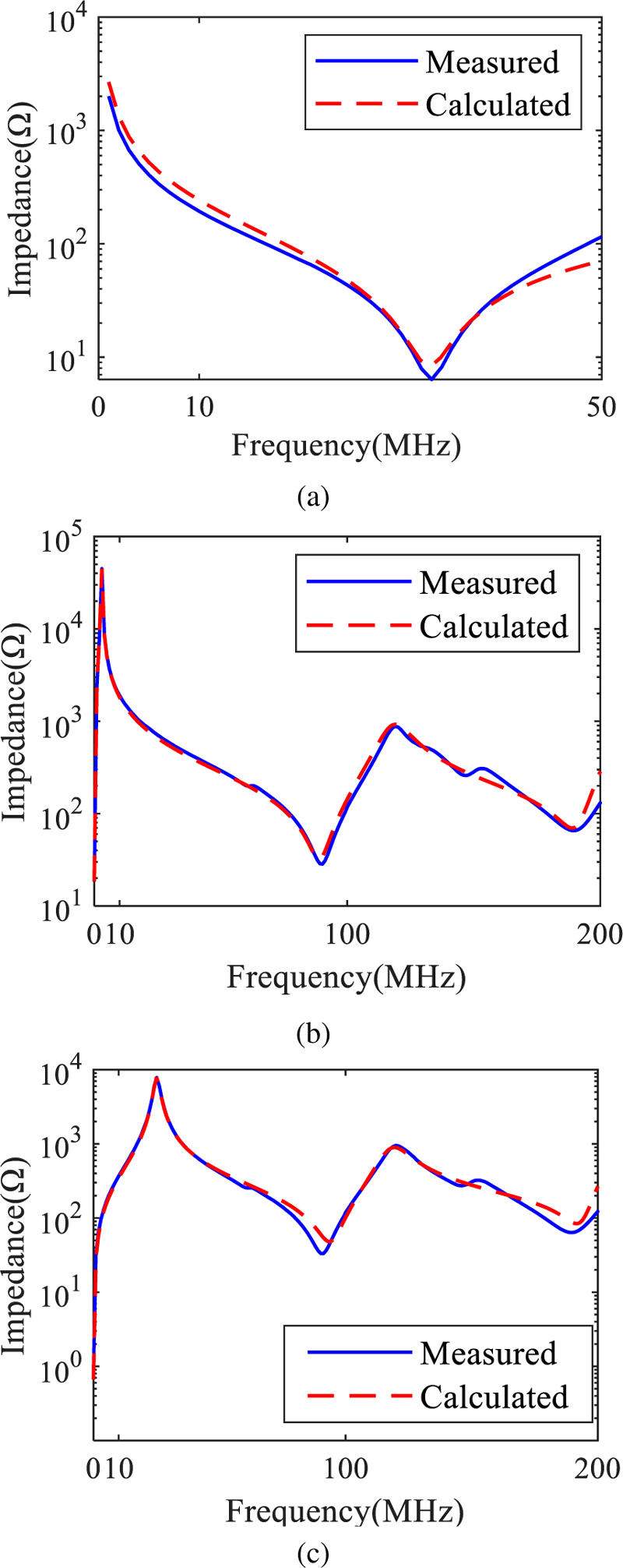
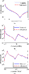
Figure 8: Comparison between simulated and measured impedance curves of transformer parameters: (a) inter-winding impedance, (b) excitation impedance, and (c) leakage impedance.
Table 4: RLC values for the high-frequency model of primary and secondary side leakage inductance
| i = 1(150 kHz-96 MHz) | i = 2(96-186 MHz) | i = 3(186-200 MHz) | |
|---|---|---|---|
| R | 1.98 k | 217.76 | 93.41 |
| L | 1.14 µH | 0.03 µH | 3.59 nH |
| C | 35.36 pF | 59.52 pF | 170.76 pF |
| R | 13.02 | 1.43 | 0.61 |
| L | 4.46 nH | 0.20 nH | 0.02 nH |
| C | 5.38 nF | 9.05 pF | 2.60 nF |
According to the calculated parameters, the models of inter-winding impedance, excitation impedance, and leakage impedance are built in the simulation software, and then the simulated and measured impedance characteristic curves are compared, respectively. The obtained results are shown in Fig. 8.
Based on the comparison results of simulated and measured impedance in Fig. 9, the established model adequately reflects the high-frequency characteristics of each parameter. However, due to simplifications and equivalent processing, some errors are inevitably present in the high-frequency model. In Figs. 8 (a-c), the maximum impedance errors are 46 , 178 , and 153 , respectively. If the impedance range measured by the three parameters is taken as the baseline, the maximum errors for the three parameters are 2.3%, 0.37%, and 1.9%, respectively.
The high-frequency model of this transformer can be obtained by substituting the parameters into the high-frequency model topology shown in Fig. 7. The excitation impedance high-frequency model consists of three R L C parallel modules in series when i=1, 2, 3, corresponding to the corresponding RLC values in Table 3. The leakage inductance high-frequency model also consists of R, L, C (R, L, C) parallel modules in series, when i = 1, 2, 3, respectively, corresponding to the corresponding RLC values in Table 4. The value of C is 118.96 pF.
V. APPLICATION OF THE HIGH-FREQUENCY TRANSFORMER MODEL IN PREDICTING CONDUCTED INTERFERENCE OF FLYBACK CONVERTERS
A. Flyback converters conducted interferenceanalysis
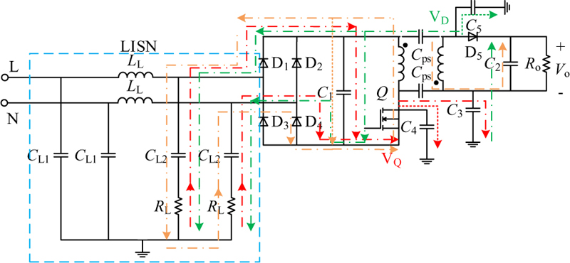
The common mode noise in flyback converters is primarily generated by the switching actions of the switching transistor and the freewheeling diode during operation [18]. When they operate, they will generate a large amount of interference noise because they are always in forward and reverse bias. The loop of common-mode interference generated by the switching transistor is shown as the red line in Fig. 9, while the loop of common-mode interference generated by the reversal diode is shown as the green line in Fig. 9 [19]. The red and green dashed lines in Fig. 9 are the common-mode interference loop and the direction of the interference signal, where V and V denote the common-mode interference voltage generated by the switching transistor and the current-continuing diode, respectively. C is the capacitance between the transformer windings. C is the capacitance of the secondary side of the transformer to the ground. C and C are the parasitic capacitance between the switching transistor, the current-continuing diode, and the heat sink, respectively.
Figure 9: Schematic diagram of interference loops of different noise sources in flyback converters.
The differential mode interference noise is mainly caused by the current ripple in the loop where the switching transistor is located in the flyback converter, which forms a voltage drop on the leakage inductance of the transformer. The differential mode interference circuit of the flyback converter is shown as the orange line in Fig. 9. The orange dashed line in Fig. 9 shows the differential mode interference circuit and the direction of the interference signal.
In the common mode interference loop and differential mode interference loop of the flyback converter, it can be seen that both the path of differential mode interference and the path of common mode interference will flow through the transformer, and the path of common mode interference will flow through the parasitic capacitance between the primary and secondary sides of the transformer, so the high-frequency model of the transformer can be accurately established to effectively predict the conducted interference of the flybackconverter.
B. Experimental platform construction
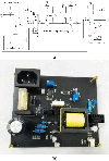
In this paper, a flyback converter is designed using the above-mentioned transformer, and then the simulated noise of the conducted disturbance is compared with the measured noise of the prototype to verify the effectiveness of the proposed transformer high-frequency modeling method and the optimization of the conducted disturbance prediction method for the conventional flyback converter. The topology of the prototype circuit is shown in Fig. 10 (a), which consists of a rectifier, control, and feedback circuits and replaces the transformer model with the high-frequency model established earlier. The fabricated flyback converter prototype is shown in Fig. 10 (b), with an input voltage of 220 V/50 Hz and an output voltage of 12 V. The main component parameters are shown in Table 5.
Figure 10: (a) Flyback converter circuit topology and (b) flyback converter prototype.
Table 5: Prototype main components parameters
| Component Parameters |
|---|
| Rectifier bridge: GBU808 |
| PWM control chip: UC3843 |
| MOSFET: 10N60 |
| Optocoupler: PC817 |
| Shunt regulator: TL431 |
| Transformer primary inductance: 332 uF |
| Transformer ratio: 37:3 |
The flyback converter circuit shown in Fig. 10 (a) is built in the simulation software. After implementing the basic functions of flyback converter simulation, the conducted interference of flyback converters will be simulated next.
C. Circuit simulation and interference waveform analysis
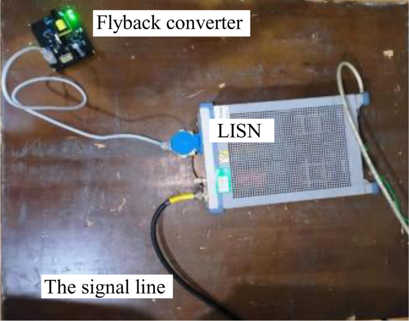
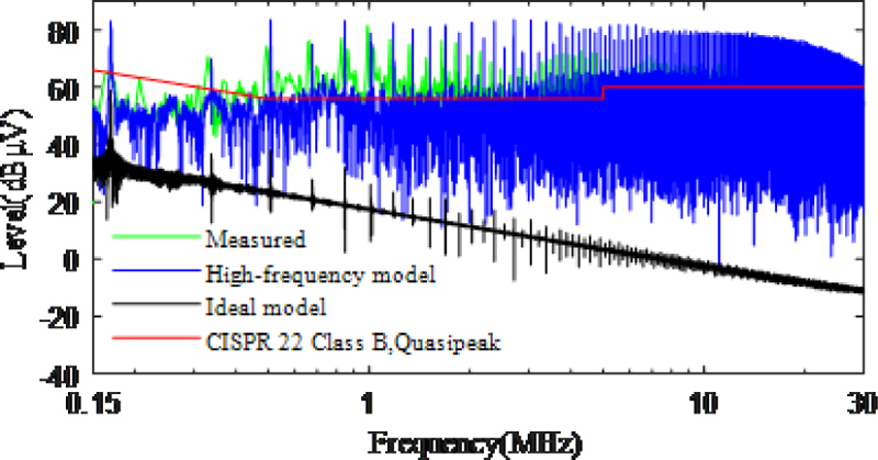
In this paper, we designed a flyback converter using the above transformer and then compared the simulated noise of conducted disturbances with the measured noise of the prototype. The test site layout of the conducted interference is shown in Fig. 11, where the signal line of LISN is connected to the spectrum analyzer, the model used for LISN is the R&S ENV216, and the test standard is CISPR 22 Class B. The simulation software employed is PSpice. The simulations are carried out with the ideal model of the transformer and the high-frequency model, and the simulated and measured conducted interference noise waveforms are shown in Fig. 12.
Figure 11: Conducted interference measurement layout.
Figure 12: Comparison of measured and simulated waveforms for conducted interference.
From Fig. 12 it can be seen that the simulation results of the transformer high-frequency model are significantly better than the simulation results of the ideal model in the frequency range of 150 kHz-30 MHz. Although the conducted interference will appear as spikes at the same frequency, the difference in the amplitude of the spikes is large, and this difference will increase with the increase in frequency. The maximum difference is greater than 80 dBuV, and it is obvious that this degree of error in the interference prediction is large. It is obvious that this level of error is not allowed in interference prediction. This shows that the transformer model greatly affects the prediction results of conducted EMI in flyback converters. A comparison between the predicted conducted interference results with the transformer high-frequency model and the prototype shows that the simulated conducted interference waveform in the frequency range of 150 kHz-5 MHz can better reflect the actual interference waveform of the flyback converter with an error within 10 dBuv, while the frequency after 5 MHz has a larger difference in the interference waveform but still reflects the actual interference waveform above the limit value. Since there is no high-frequency modeling of the switching transistor and current-continuing diodes in this paper, and there may also be crosstalk in the circuit, coupled with the limits of the measurement instruments and experimental conditions, this inevitably leads to errors between the measured and simulated conducted interference waveforms. However, the flyback converter simulation circuit using the transformer high-frequency model is better able to predict the actual conducted disturbance waveform over the entire frequency range. Thus, the design and optimization of flyback converters can be facilitated, especially in terms of reducing the amount of labor and resources required for EMI correction.
VI. CONCLUSION
This paper presents a method for predicting conducted disturbances in flyback converters based on the high-frequency transformer model. Through the analysis of the conducted disturbance of the flyback converter, it is known that the transformer model has a great influence on the prediction of conducted disturbance. In order to accurately predict the conduction interference of a flyback converter, this paper proposes a new transformer model topology based on the traditional inductor model and the three-capacitor model and extracts the parameters of the transformer model using SOMA. The high-frequency transformer model is used instead of the ideal model for the optimization of the conduction interference prediction method of flyback converters. The predictions based on the conventional and optimized conduction interference prediction methods are carried out, and the prediction results are compared with the measured results of the prototype to verify the effectiveness of the proposed transformer high-frequency modeling method and the conduction interference prediction method of the flyback converter. The results show that the optimized prediction results are significantly better than the traditional prediction and can accurately reflect the actual interference level of the flyback converter. The proposed method is also applicable to other high-frequency transformer modeling and the interference prediction of flyback converters with transformers.
ACKNOWLEDGMENT
This paper is supported by Open Fund of State Key Laboratory of Power Grid Environmental Protection (GYW51202301426).
REFERENCES
[1] J. Dong, W. Chen, and Z. Lu, “Modeling and analysis of capacitive effects in high-frequency transformer of SMPS,” Proceedings of the Chinese Society of Electrical Engineering, vol. 27, no. 31, pp. 121-126, 2007.
[2] W. M. Colonel and T. Mclyman, Transformer and Inductor Design Handbook, Boca Raton, FL: CRC Press, 2004.
[3] Z. De Grève, O. Deblecker, and J. Lobry, “Fast computation of R L parameters of high frequency multi-winding magnetic components,” COMPEL-The International Journal for Computation and Mathematics in Electrical and Electronic Engineering, vol. 30, no. 6, pp. 1914-1926, 2011.
[4] G. Antonini, A. Orlandi, and C. R. Paul, “Internal impedance of conductors of rectangular cross section,” IEEE Transactions on Microwave Theory and Techniques, vol. 47, no. 7, pp. 979-985, July 1999.
[5] H. Y. Lu, J. G. Zhu, and V. S. Ramsden, “Comparison of experimental techniques for determination of stray capacitances in high frequency transformers,” 2000 IEEE 31st Annual Power Electronics Specialists Conference. Conference Proceedings, vol. 3, pp. 1645-1650, 2000.
[6] X. Margueron and J. P. Keradec, “Identifying the magnetic part of the equivalent circuit of n-winding transformer,” 2005 IEEE Instrumentation and Measurement Technology Conference Proceedings, pp. 1064-1069, 2005.
[7] R. C. Degeneff, M. R. Gutierrez, and P. J. McKenny, “A method for constructing reduced order transformer models for system studies from detailed lumped parameter models,” IEEE Transactions on Power Delivery, vol. 7, no. 2, pp. 649-655, Apr. 1992.
[8] B. Cogitore, J. P. Keradec, and J. Barbaroux, “The two-winding transformer: an experimental method to obtain a wide frequency range equivalent circuit,” IEEE Transactions on Instrumentation and Measurement, vol. 43, no. 2, pp. 364-371, Apr. 1994.
[9] Hai Yan Lu, Jian Guo Zhu, and S. Y. R. Hui, “Experimental determination of stray capacitances in high frequency transformers,” IEEE Transactions on Power Electronics, vol. 18, no. 5, pp. 1105-1112, Sep. 2003.
[10] C. Liu, “High voltage high frequency transformer wide-frequency modeling method and its application research,” Ph.D. dissertation, Dept. of Electrical Engineering, North China Electric Power University, Beijing, China. 2017.
[11] L. Xie, X. Ruan, and Z. Ye, “Equivalent noise source: An effective method for analyzing common-mode noise in isolated power converters,” IEEE Transactions on Industrial Electronics, vol. 63, no. 5, pp. 2913-2924, May 2016.
[12] M. Ferber, C. Vollaire, L. Krähenbühl, J.-L. Coulomb, and J. A. Vasconcelos, “Conducted EMI of DC–DC converters with parametric uncertainties,” IEEE Transactions on Electromagnetic Compatibility, vol. 55, no. 4, pp. 699-706, Aug.2013.
[13] H. Chen and G. Liu, “Determination of the width of shielding foil in sandwiched winding transformer for minimizing common mode EMI of flyback converters,” IEEE Transactions on Electromagnetic Compatibility, vol. 62, no. 2, pp. 639-642, Apr. 2020.
[14] J. Liu, L. Zhou, Y. Luo, X. Huang, and G. Wu, “Dielectric frequency response of oil-paper composite insulation with transient moisture distribution,” IEEE Transactions on Dielectrics and Electrical Insulation, vol. 20, no. 4, pp. 1380-1387, Aug. 2013.
[15] M. Zhou, Y. Zhao, C. Zhang, X. Liu, X. Wu, Y. Sun, and W. Yan, “Predicting the impact of transient voltage suppressor used for ESD protection on the low noise amplifier,” Microelectronics Journal, vol. 113, July 2021.
[16] Y. Pei, H. Ma, M. Zhou, W. Yan, and C. Zhang, “High-frequency characteristic modeling of common mode chokes based on self-organizing migration algorithm,” Electronic Components and Materials, vol. 42, no. 02, pp. 200-205, Feb. 2023.
[17] P. R. Wilson and A. D. Brown, “Effective modeling of leakage inductance for use in circuit simulation,” 2008 Twenty-Third Annual IEEE Applied Power Electronics Conference and Exposition, pp. 391-395, 2008.
[18] F. Hubert, P. Dorsch, D. Kuebrich, T. Duerbaum, and S. J. Rupitsch, “Piezoelectric EMI filter for switched-mode power supplies,” IEEE Transactions on Power Electronics, vol. 36, no. 6, pp. 6624-6643, June 2021.
[19] D. Jiaqi, Y. Ru, L. Zuolian, Y. Hong, and J. Hai, “Modeling and analysis of conducted EMI on flyback converter using power management IC with chaotic suppression EMI,” 2020 22nd European Conference on Power Electronics and Applications (EPE’20 ECCE Europe), pp. 1-10, 2020.
BIOGRAPHIES

Mengxia Zhou received the M.S. degree in electrical engineering and the Ph.D. degree in physics and electronics from Nanjing Normal University, in 2018 and 2021, respectively. His main research interests include electromagnetic compatibility, electromagnetic environment effect, and high frequency device modeling.

Bin Cheng was born in Anhui, China. He received his B.E. degree in electrical engineering from Anhui University of Technology in 2021. He is currently pursuing a M.S. degree in electrical engineering at Nanjing Normal University. His current research interests include high frequency device modeling, switched-mode power supplies, and electromagnetic compatibility.

Jianben Liu graduated from Huazhong University of Science and Technology with a Doctor’s degree in Electrical engineering in 2013. He is mainly engaged in the research of power electronics technology, power quality and electromagnetic environment of power systems.

Yakang Pei was born in China. He completed his studies in electrical engineering and its automation at the Haibin College of Beijing Jiaotong University in Cangzhou, Hebei, China in 2019, and received his bachelor’s degree in engineering. He is a master student at Nanjing Normal University with research interests in electromagnetic compatibility and high frequency device modeling.

Ruining Yao received bachelor’s degree in engineering with electrical machine and its control major from Hunan university in 1997. His main research interests include electrical machine, electromagnetic environment effect, electromagnetic compatibility.

Liu Yan is a senior engineer. Her research interests are power grid remote sensing monitoring and line operation and maintenance.

Feng Li obtained his Ph.D. degree from Southeast University, China in 2021. After Ph.D. graduation, he joined school of electrical and automatic engineering, Nanjing Normal University, China. His research areas include power system modelling and simulation, power system stability analysis and control.
ACES JOURNAL, Vol. 39, No. 1, 81–90
doi: 10.13052/2024.ACES.J.390110
© 2024 River Publishers
