Balanced Filtering Power Divider based on Odd-mode Hybrid Microstrip and Slotline Spoof Surface Plasmon Polaritons
Yi Song and Anxue Zhang
School of Information and Communications Engineering
Xi’an Jiaotong University, Xi’an 710049, China
yi_song17@hotmail.com, anxuezhang@mail.xjtu.edu.cn
Submitted On: June 23, 2023; Accepted On: September 8, 2023
ABSTRACT
In this paper, an ultra-wideband balanced filtering power divider (B-FPD) with high common mode (CM) suppression level is proposed. The B-FPD is designed based on the odd mode spoof surface plasmon polaritons (SSPPs), which are constructed by the hybrid folded microstrip and slotline (HFMS) structure. Firstly, the dispersion characteristic and electric field distribution of the HFMS SSPP unit cell are investigated, which can decrease the upper cut-off frequency for size reduction of nearly 50%. Next, an equal balanced power divider with low cut-off frequency is proposed based on the microstrip-to-slotline transition structure and slotline Y-junction. Then, the balanced power divider is used to excite the odd mode of HFMS SSPP structure. An equal B-FPD with center frequency of 4.0 GHz is implemented, and the 3-dB bandwidth covers 0.9 to 7.0 GHz. Finally, the B-FPD with advantages of high CM suppression level and compact size is fabricated and measured.
Index Terms: balanced filtering power divider, common mode suppression, spoof surface plasmon polariton.
I. INTRODUCTION
With the developments of modern mobile communication, radio frequency (RF) communication systems have attracted extensive attention. Hence, researchers have paid much efforts in implementing excellent RF devices, such as antennas, power dividers, bandpass filters, and phase shifters. Power dividers and filtering power dividers, as the crucial components of RF circuit system, can realize functions of power distribution and frequency selection, respectively [1–5].
Spoof surface plasmon polariton (SSPP) structure can support the surface wave alike surface plasmon polaritons (SPPs) at microwave frequency, and the SSPPs show the similar characteristics of electromagnetic field confinement, upper cut-off frequency with the SPP at optical frequency band [6, 7]. Hence, in recent years, the SSPP transmission lines have been widely adopted for designing microwave filters [8, 9], diplexers [10], phase shifters [11, 12], antennas [13], splitters [14–17], etc.
In particular, some well-designed power dividers are reported based on SSPP structure fed by the coplanar waveguide (CPW) [14–16], and double-sided parallel spoof surface plasmon polariton transmission line (DSP-SSPP-TL) [17]. In [15], a four-way SSPP splitter is designed by the SSPP transmission line. The transition structure constructed by the long axis of a half oval ring is used to match the wave vector between the CPW mode and the SSPP mode. Furthermore, a beam splitter with multi-band rejection is implemented based on SSPP structure with T-shaped decoration [16]. In addition, the DSP-SSPP-TL is also adopted for designing balanced dividers with ultra-wideband isolation by loading the lumped resistors [17].
Recently, the multifunctional integrated devices, such as filtering power dividers (FPDs) have been widely reported, which can not only achieve power distribution and frequency selection functions simultaneously but also avoid the additional power loss and size increase caused by the devices cascade [18–23]. Hence, several FPDs are proposed based on SSPP structure fed by CPW [18], slotline SSPP unit cells [19, 20], and hybrid SSPP and substrate integrated waveguide (SIW) structures [21–23]. In [19], an ultra-wideband FPD is designed based on the quasi Y-junction slotline SSPP transmission line constructed by the corrugated grooves. The odd SSPP mode is excited by the microstrip-to-slotline convertor. Besides, the compact FPD implemented by the hybrid SSPP and SIW achieves independent control of the upper and lower stopbands [23].
Balanced microwave components, such as balanced filters [24] and balanced filtering dividers [25] base on the microstrip resonator, have drawn extensive attention due to the excellent advantages of common mode (CM) noise rejection. It is essential to achieve compact size, good filtering function, and high CM suppression level.
In this paper, a hybrid folded microstrip and slotline (HFMS) SSPP unit cell is proposed, whose fundamental mode is odd mode. The dispersion curves show that the HFMS unit cell can lower the upper cut-off frequency for size miniaturization of nearly 50%. And a highpass balanced power divider is designed by microstrip-to-slotline transition feeding structure and slotline Y-junction. Then, the balanced power divider is adopted to excite the odd mode of the HFMS SSPP structure. Finally, an equal balanced FPD with high CM suppression level is implemented by the Rogers 5880 substrate with the relative dielectric constant of 2.2, thickness of 0.5 mm, and loss tangent of 0.0009. And the in-band minimum insertion loss is 1.5 dB.
II. CHARACTERISTIC OF THE SSPP UNIT
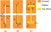
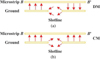
Figure 1 shows configurations of three types of SSPP unit cells. In Fig. 1 (a), the traditional slotline SSPP unit cell is presented. The orange metal and white strips represent the ground plane at bottom layer and slotline, respectively. Figure 1 (b) shows the hybrid microstrip and slotline (HMS) SSPP unit cell, and the yellow strip represent the metal microstrip on the top layer. To further reduce the physical dimension, the top metal microstrip is folded and the HFMS SSPP unit cell is shown in Fig. 1 (c).
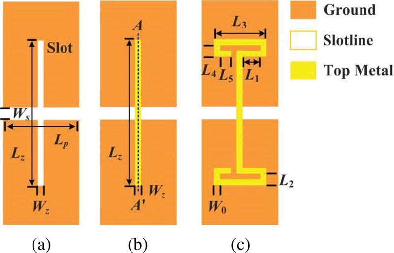
Figure 1: Configuration of the SSPP unit cells: (a) Type A: traditional slotline, (b) Type B: Hybrid microstrip and slotline, and (c) Type C: Hybrid folded microstrip and slotline.
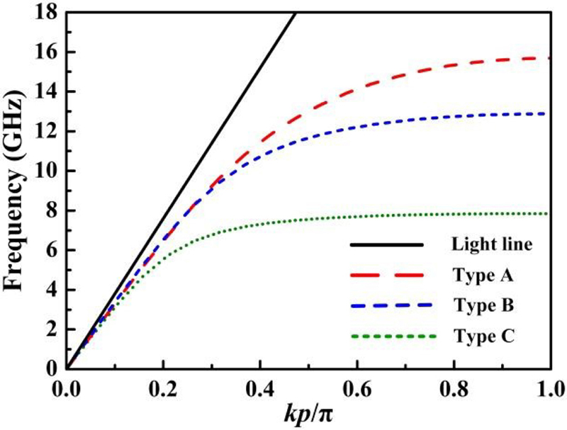
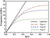
Figure 2: Simulated dispersion curves of the fundamental mode of three types of SSPP unit cells.
The comparisons of simulated dispersion curves of the fundamental mode of three types of SSPP unit cells are shown in Fig. 2. The physical dimensions of SSPP unit cells are as follows: W = 0.3, W = 0.3, W = 0.8, L = 7, L = 3.8, L = 0.9, L = 0.6, L = 2.7, L = 0.6, L = 0.6 (unit: mm). The upper cut-off frequencies of traditional slotline SSPP unit cell and HMS SSPP unit cell are 15.7 GHz and 12.9 GHz, respectively. Furthermore, the upper cut-off frequency can be further reduced to 7.8 GHz by the HFMS SSPP unit cell. Hence, a size reduction of nearly 50.0% can be achieved.
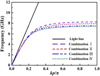
Table 1: Dimensions of HFMS SSPP cells (unit: mm)
| Combination | L | W | W | L | L | W |
| I | 4.0 | 0.3 | 0.8 | 3.8 | 7.2 | 0.3 |
| II | 5.4 | 0.5 | 0.8 | 3.8 | 7.2 | 0.3 |
| III | 5.4 | 0.3 | 0.8 | 3.8 | 7.2 | 0.3 |
| IV | 5.4 | 0.3 | 1.0 | 3.8 | 7.2 | 0.3 |
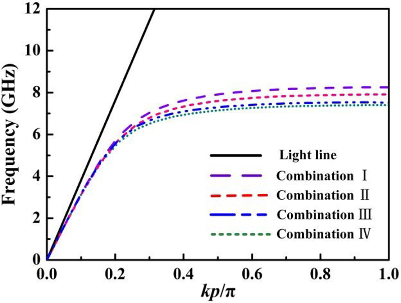
Figure 3: Comparison of simulated dispersion curves of the HFMS SSPP unit cell with different dimensions.
The upper cut-off frequency of the HFMS SSPP unit cell can be adjusted by the physical dimensions. The effects of parameters L, W, and W are investigated, and four groups of physical dimensions are listed in Table 1, where L = L + L + L + L + L. Figure 3 shows the simulated dispersion curves with different dimensions. It can be concluded from Fig. 3 that (1) the upper cut-off frequency can be reduced by increasing the length L of microstrip transmission line; (2) the upper cut-off frequency can be reduced by decreasing the width W of the microstrip; and (3) the increase of width W of the slotline can allow upper cut-off frequency shift slightly toward lower frequency. Hence, the upper cut-off frequency can be easily designed.
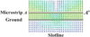
The differential mode (DM) filtering function can be achieved by the odd mode of the SSPP transmission line. Hence, the electric field distribution of the fundamental mode of HFMS SSPP unit cell is investigated, and its cross-section view is shown in Fig. 4. It can be observed that the electric fields on two sides of the slotline are out-of-phase. Hence, the odd fundamental mode can be used to achieve a DM filtering function with upper cut-off frequency. In particular, the symmetric plane AA is equivalent to an electric wall, and electric field distribution within the slotline is in phase.
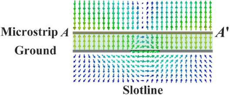
Figure 4: Cross-section view (AA) of the simulated electric field distribution of the fundamental mode of the HFMS SSPP unit cell.
III. SLOTLINE BALANCED POWER DIVIDER
In this section, a slotline balanced highpass filter is designed based on microstrip-to-slotline transition feeding structure and slotline transmission line. Then, a slotline balanced power divider with highpass characteristic is designed by using the slotline Y-junction, which can separate the common input port into two output ports.
Figure 5 shows the configuration of the slotline balanced highpass filter. The microstrip-to-slotline transition feeding structure is adopted for exciting the slotline stepped impedance transmission line. The corner cut is introduced to reduce the impedance discontinuity and signal reflection. The slotline stepped impedance structure can increase the freedom in adjusting the matching and without affecting the upper cut-off frequency of the SSPP unit cell. The matching of the feeding structure can be controlled by adjusting the length L of slotline, width W of slotline, distance d between feeding line and circular slotline, and the radius R of the circular slotline. Since a balanced FPD with three gradient HFMS SSPP unit cells and three identical SSPP unit cells will be designed in the next section, the lengths of slotline L, L, and L are all set as 3 L mm.
Figure 6 shows a cross-section view of electric field distributions of the feeding structure under DM and CM excitation. As shown in Fig. 6 (a), the electric field distribution under DM excitation is identical to that of the fundamental mode. Hence, the odd mode of the SSPP unit cell can be excited. Under CM excitation, the symmetric plane BB corresponds to a magnetic wall. The electric field distribution within the slotline is out of phase, as shown in Fig. 6 (b). Hence, the CM signals will cancel out and the feeding structure exhibits intrinsic CM suppression ability [24].
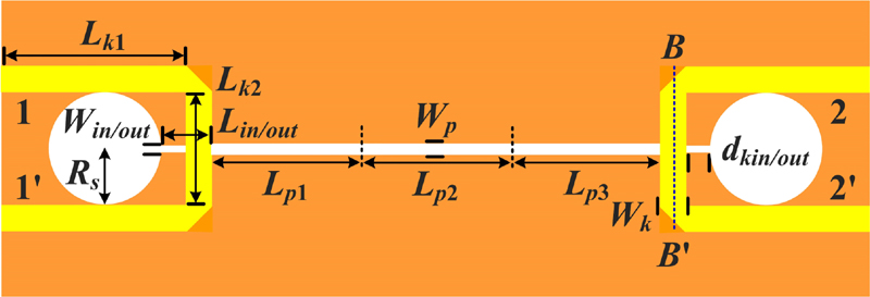
Figure 5: Configuration of the slotline balanced highpass filter. (All dimensions are in mm: L=23.5, L=14, L=3, L=34.8, W=1.5, W=0.6, W = 0.8, R = 7, d = 1.5).
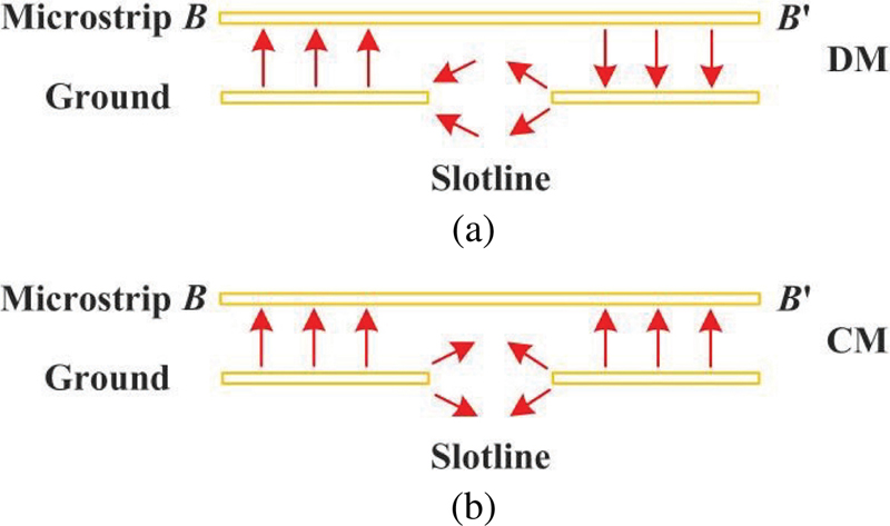
Figure 6: Cross-section view (BB) of electric field distribution of the transition feeding structure. (a) DM excitation; (b) CM excitation.
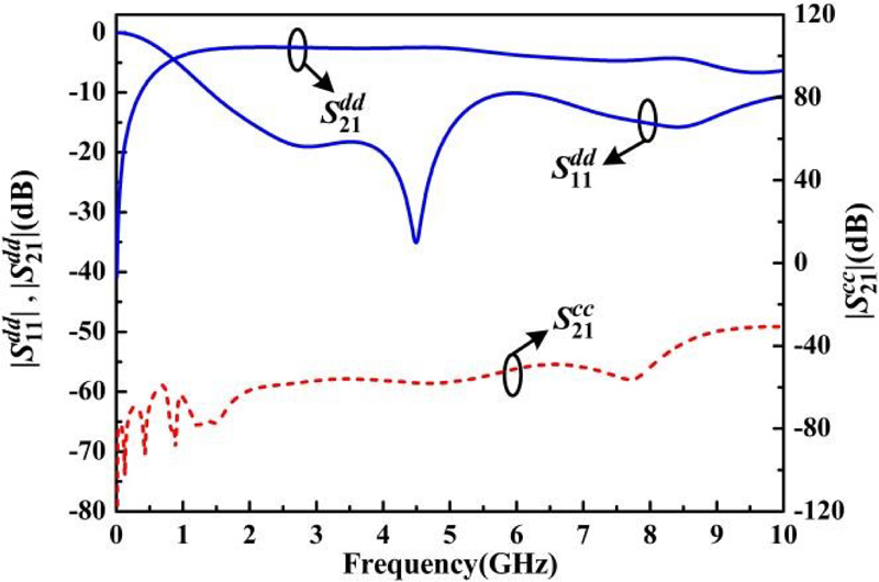
Figure 7: Simulated results of transmission and reflection characteristics of the slotline balanced highpass filter.
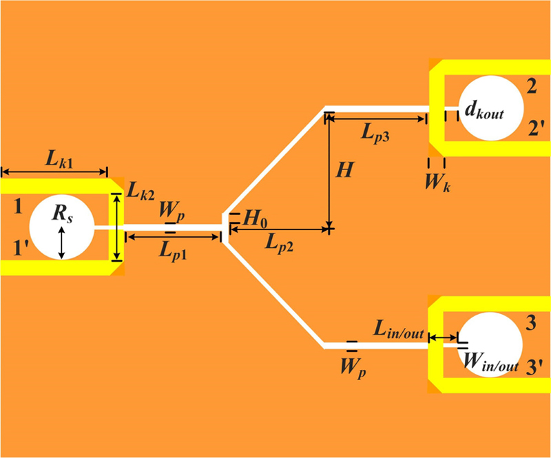
Figure 8: Configuration of the slotline balanced highpass divider. (All dimensions are in mm: L=23.5, L=14.0, L=3.0, L=L=L=11.4, W=1.5, W=0.6, W=0.8, R = 7.0, d = 1.5, H = 0.8, H = 13.5).
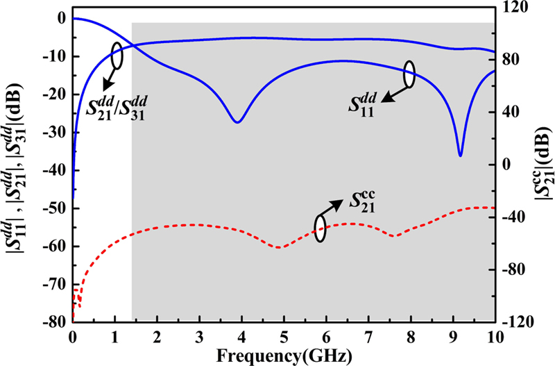
Figure 9: Simulated results of the slotline balanced highpass divider.
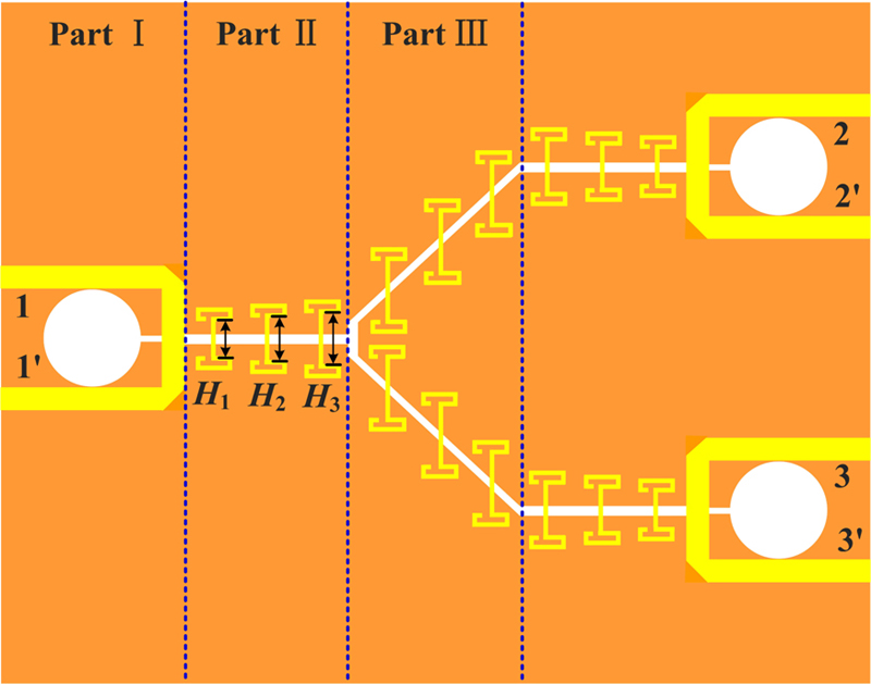
Figure 10: Configuration of the SSPP-based balanced filtering divider. (All dimensions are in mm: H=3.4, H=4.2, H=5.0).
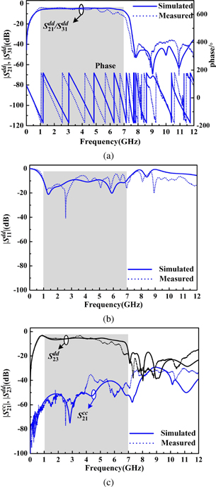
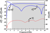
Figure 11: Transmission and reflection characteristics of the balanced filtering divider: (a) S/S/phase, (b) S, (c) S/S.
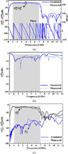
Figure 7 presents the simulated transmission and reflection characteristics of the slotline balanced filter. Under DM excitation, a highpass filtering function with low cut-off frequency of 1.0 GHz is achieved duo to the microstrip-to-slotline feeding structure with a highpass characteristic. And the in-band return loss is above 11.5 dB within 7.0 GHz. The in-band minimum insertion loss is 2.5 dB, and the relatively large insertion loss is caused by the radiation loss of the slotline structure. In addition, the low cut-off frequency of the balanced highpass filter can be adjusted by the radius R, and it will move toward lower frequency as the value of R increases. Under CM excitation, the in-band CM suppression level is above 50.0 dB, the 40.0 dB CM suppression level can be up to 12.0 GHz.
Based on the slotline balanced filter, an equal balanced power divider with low cut-off frequency is implemented, as shown in Fig. 8. The slotline Y-junction is adopted to replace the slotline transmission line L. The horizontal length of the slotline Y-junction is equal to L. The signals from input port 1/1’ will be allocated to ports 2/2 and 3/3 with equal power ratio. And the matching between input port 1/1 and 2/2, 3/3 can be adjusted by parameters H and H. The final physical dimensions of balanced power divider are listed in the annotation of Fig. 8.
Figure 9 shows the DM and CM simulated transmission and reflection characteristics of the balanced divider. Under DM excitation, a balanced power divider with low cut-off frequency of 1.5 GHz is achieved. The in-band minimum insertion loss of the balanced power divider is 2.36 dB, with 3-dB power division loss excluded. And the return loss is above 11.2 dB within 7.0 GHz. Under CM excitation, the CM suppression level is above 44.0 dB.
IV. BALANCED FILTERING DIVIDER BASED ON SSPP
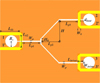
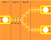
On this basis, the balanced filtering power divider (FPD) is implemented, as shown in Fig. 10. Part I is the feeding structure constructed by microstrip-to-slotline transition structure. Part II is momentum matching conversion structure constructed by three gradient HFMS SSPP unit cells, which can match the wave vector between TE mode and SSPP mode. The TE mode transmitted from the feeding structure will be converted to SSPP mode. The matching can be adjusted by the length difference between adjacent SSPP unit cells. Part III is a SSPP transmission line, which consists of three identical HFMS unit cells. The SSPP transmission line can support the transmission of SSPP waves and provide the upper cut-off frequency for achieving filtering function.
Figure 11 presents the simulated results of the balanced FPD under DM and CM excitation. Under DM excitation, a balanced FPD with center frequency of 4.0 GHz and 3-dB fractional bandwidth of 152.0% is achieved. The in-band insertion loss is 1.7 dB, with 3 dB power division loss excluded, and the in-band return loss is above 9.2 dB. Benefiting from the field confinement ability of the SSPP structure, the insertion loss is reduced by nearly 0.7 dB. The isolation between two output ports is above 6 dB, which is poor due to the lack of an isolation resistor. Under CM excitation, the in-band CM suppression is above 40.0 dB.
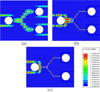
Figure 12 presents the electric field distributions of the balanced FPD under DM and CM operation. Under DM excitation, it can be observed from Fig. 12 (a) that the DM signals can transfer from input port 1/1 to output ports 2/2 and 3/3 within the passband, for example at 1.5 GHz. On the contrary, the DM signals out of the passband cannot transmit to the output ports, as shown in Fig. 12 (b). Under CM excitation, the CM signals are rejected by microstrip-to-slotline transition feeding structure, as shown in Fig. 12 (c).
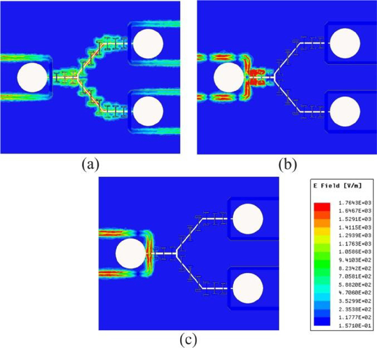
Figure 12: Simulated E-field distribution of the balanced filtering divider at (a) 1.5 GHz, (b) 8.0 GHz under DM excitation, and (c) 4.0 GHz under CM excitation.
V. IMPLEMENTATION AND MEASUREMENT
In order to verify the methodology, the balanced FPD is fabricated on the Rogers 5880 substrate. The photographs of top and bottom view of the fabricated B-FPD are shown in Fig. 13. The total circuit size is 80.0 mm 70.0 mm 0.5 mm, which amounts to 1.45 1.27 0.006, where is the guided wavelength at the center frequency of 4.0 GHz.
Table 2: Comparisons with previous SSPP-based filtering dividers
| Ref. | Circuit Size () | f (GHz) | FBW (%) | IL (dB) | Structure Type | Operation | CMRR/dB |
| [18] | / | 5.3 | 105.0% | 1.8 | CPW | Single-ended | No |
| [20] | 0.22 | 3.6 | 99.0% | 1.4 | Slot | Single-ended | No |
| [22] | / | 6.0 | 66.0% | 1.0 | SIW | Single-ended | No |
| [23] | 1.5 0.67 | 10.0 | 40.0% | 0.8 | SIW | Single-ended | No |
| This work | 1.45 1.27 | 4.0 | 152.0% | 1.7 | Microstrip + Slot | Balanced | 50 |
| : wavelength of the guided wave, f: center frequency, FBW: 3-dB fractional bandwidth, IL: insertion loss, CMRR: common mode rejection ratio. | |||||||
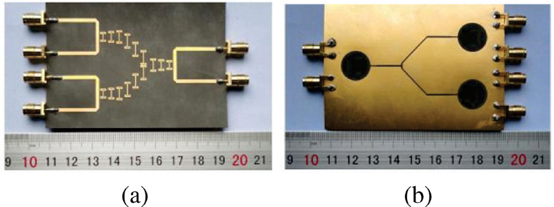
Figure 13: Photographs of the (a) top and (b) bottom views of the fabricated balanced filtering divider.
The fabricated balanced B-FPD is measured by a four-port vector network analyzer, and the measured results are shown in Fig. 11. Under the DM operation, the measured minimum insertion loss is 1.6 dB, and in-band return loss is above 5.2 dB. Under the CM operation, the in-band CM suppression level is above 35.0 dB. The differences between measured and simulated results may result from fabrication tolerances, deformations caused by fabrication and test.
Table 2 shows comparisons with the published SSPP-based filtering power divider. The proposed balanced FPD shows the advantages of relatively compact size and good CM suppression level. In addition, the balanced FPD based on SSPP is easier to fabricate.
VI. CONCLUSION
In this paper, an odd-mode SSPP structure constructed by a HFMS structure is investigated. Then, the microstrip-to-slotline transition feeding structure and slotline Y-junction are adopted for designing the balanced power divider, which can achieve controllable low cut-off frequency, equal power distribution ratio, and intrinsic CM suppression ability. Finally, the balanced FPD is designed by adopting the balanced power divider to feed the HFMS SSPP structure. The upper cut-off frequency can be controlled by the physical dimensions of the SSPP unit cell. The balanced FPD shows the advantages of relatively compact size and high CM suppression level.
ACKNOWLEDGMENT
This work was supported in part by the National Key R&D Program of China under Grant 2020YFA0709802, and in part by the “Siyuan Scholar” Fellowship of XJTU.
REFERENCES
[1] G. Dong, B. Zhang, W. Wang, and Y. Liup, “Compact wideband filtering power dividers based on short-circuited stubs,” Applied Computational Electromagnetics Society (ACES) Journal, vol. 34, pp. 141-147, 2019.
[2] Z. Qiao, Y. Chen, C. Feng, and W. Wang, “Compact multi-mode filtering power divider with high selectivity, improved stopband and in-band isolation,” Applied Computational Electromagnetics Society (ACES) Journal, vol. 35, pp. 936-940, 2020.
[3] W. J. Shen, Y. Han, W. R. Chen, D. Jiang, S. Luo, and T. M. Bai, “Design of electronically controlled filter power divider based on liquid crystal,” Applied Computational Electromagnetics Society (ACES) Journal, vol. 37, pp. 93-101, 2022.
[4] S, Roshani, S. I. Yahya, B . M. Alameri, Y. S. Mezaal, L. W. Liu, and S. Roshani, “Filtering power divider design using resonant LC branches for 5G low-band applications,” Sustainability, vol. 14, Article ID 12291, 2022.
[5] S, Roshani, S. I. Yahya, J. Rastad, Y. S. Mezaal, L. W. Liu, and S. Roshani, “Design of a filtering power divider with simple symmetric structure using stubs,” Symmetry, vol. 14, Article ID 1973, 2022.
[6] X. Gao, L. Zhou, Z. Liao, H. F. Ma, and T. J. Cui, “An ultra-wideband surface plasmonic filter in microwave frequency,” Appl. Phys. Lett., vol. 104, Article ID 191603, 2014.
[7] L. Tian, Z. Zhang, J. Liu, K. Zhou, Y. Gao, and S. Liu, “Compact spoof surface plasmon polaritons waveguide drilled with L-shaped grooves,” Opt. Exp., vol. 24, pp. 28693-28703, 2016.
[8] D. F. Guan, P. You , Q. Zhang, K Xiao, and S.-W. Yong, “Hybrid spoof surface plasmon polariton and substrate integrated waveguide transmission line and its application in filter,” IEEE Trans. Microw. Theory Techn., vol. 65, pp. 4925-4931, 2017.
[9] Y. Liu and K.-D. Xu, “Bandpass filters using grounded stub-loaded microstrip periodic structure for suppression of modes,” J. Phys. D: Appl. Phys., vol. 55, Article ID 425104, 2022.
[10] Y. Cui, K.-D. Xu, Y. Guo, and Q. Chen, “Half-mode substrate integrated plasmonic waveguide for filter and diplexer designs,” J. Phys. D: Appl. Phys., vol. 55, Article ID 125104, 2022.
[11] C. Ding, F.-Y. Meng, J.-Q. Han, H.-L. Mu, Q.-Y. Fang, and Q. Wu, “Design of filtering tunable liquid crystal phase shifter based on spoof surface plasmon polaritons in PCB technology,” IEEE Trans. Compon. Packag. Manuf. Technol., vol. 9, pp. 2418-2826, 2019.
[12] A. R. Moznebi and K. Afrooz, “Wideband compact phase shifter based on hybrid half-mode substrate integrated waveguide and spoof surface plasmon polariton,” J. Phys. D: Appl. Phys., vol. 55, Article ID 155203, 2022.
[13] Q. Li, Y. Yin, X. Chen, and K.-D. Xu, “A frequency-controlled wide-angle scanning antenna based on spoof surface plasmon polariton,” IEEE Photonics Technol. Lett., vol. 34, pp. 1300-1303, 2022.
[14] J. Wang, L. Zhao, Z. C. Hao, X. Shen, and T. J. Cui, “Splitting spoof surface plasmon polaritons to different directions with high efficiency in ultra-wideband frequencies,” Opt. Lett., vol. 44, pp. 3374-3377, 2019.
[15] S.-Y. Zhou, S.-W. Wong, J.-Y. Lin, L. Zhu, Y. J. He, and Z.-H. Tu, “Four-way spoof surface plasmon polaritons splitter/combiner,” IEEE Microw. Wirel. Compon. Lett., vol. 29, pp. 98-100, 2019.
[16] A. Aziz, Y. Fan, P. H. He, H. C. Zhang, I. Ali, W. X. Tang, and T. J. Cui, “Spoof surface plasmon polariton beam splitters integrated with broadband rejection filtering function,” J. Phys. D, Appl. Phys., vol. 54, Article ID 335105, 2021.
[17] M. Li, Y. Wu, M. Qu, Q. Li, and Y. Liu, “A novel power divider with ultra-wideband harmonics suppression based on double-sided parallel spoof surface plasmon polaritons transmission line,” Int. J. RF Microw. Comput.-Aided Eng., vol. 28, Article ID e21231, 2018.
[18] E. Farokhipour, N. Komjani, and M. A. Chaychizadeh, “An ultra-wideband three-way power divider based on spoof surface plasmon polaritons,” J. Phys. D, Appl. Phys., vol. 124, Article ID 235310, 2018.
[19] H.-T. Xu, D.-F. Guan, Z.-B. Yang, Q. Zhang, L. Liu, S. Xu, and S.-W. Yong, “An ultra-wideband out-of-phase power divider based on odd-mode spoof surface plasmon polariton,” Int. J. RF Microw. Comput.-Aided Eng., vol. 31, Article ID e22583, 2021.
[20] A. R. Moznebi, K. Afrooz, and A. Arsanjani, “Broadband bandpass filter and filtering power divider with enhanced slow-wave effect, compact size, and wide stopband based on butterfly-shaped spoof SPPs,” AEU Int. J. Electron. Commun., vol. 145, Article ID 154084, 2022.
[21] B. C. Pan, P. Yu, B. J. Guo, Y. F. Qiao, and G. Q. Luo, “Unequal bandpass filtering power divider based on hybrid HMSIW-SSPP modes,” Front. Phys., vol. 10, Article ID 851150, 2022.
[22] A. R. Moznebi and K. Afrooz, “Bandwidth enhancement of a half-mode substrate integrated waveguide filtering power divider using spoof surface plasmon polariton,” J. Phys. D: Appl. Phys., vol. 55, Article ID 025103, 2022.
[23] B. C. Pan, P. Yu, Z. Liao, F. Zhu, and G. Q. Luo, “A compact filtering power divider based on spoof surface plasmon polaritons and substrate integrated waveguide,” IEEE Microw. Wireless Compon. Lett., vol. 32, pp. 311-314, 2022.
[24] M. Z. Du, Y. J. Feng, K. Chen, and J. M. Zhao, “Filtering microwave differential signals through odd-mode spoof surface plasmon polariton propagation,” J. Phys. D: Appl. Phys., vol. 53, Article ID 165105, 2020.
[25] Q. Liu, J. Wang, L. Zhu, G. Zhang, and W. Wu, “Design of a new balanced-to-balanced filtering power divider based on square patch resonator,” IEEE Trans. Microw. Theory Techn., vol. 66, pp. 5280-5289, 2018.
BIOGRAPHIES

Yi Song received the B.S. degree in communication engineering and the M.S. degree in communication and information system from East China Jiaotong University, Nanchang, China, in 2015 and 2018, respectively. He is currently pursuing the Ph.D. degree in electromagnetic field and microwave technology at Xi’an Jiaotong University, Xi’an, China. His current research interests include microwave passive components.

Anxue Zhang received the B.S. degree in electrical engineering from Henan Normal University, in 1996, and the M.S. and Ph.D. degrees in electromagnetic and microwave engineering from Xi’an Jiaotong University, in 1999 and 2003, respectively. He is currently a professor with Xi’an Jiaotong University. His main research fields include metamaterials, RF and microwave circuit design, antennas, and electromagnetic wavepropagation.
ACES JOURNAL, Vol. 38, No. 7, 532–538
doi: 10.13052/2023.ACES.J.380709
© 2023 River Publishers