A Miniaturized UWB Bandpass Filter Employing Multi-Stub-Loaded Short-Circuited Stepped Impedance Ring Resonator
Guangyong Wei, Yunxiu Wang, Jie Liu, and Haiping Li
1School of Electronic and Information Engineering
China West Normal University, Nanchong, 637009, China
1772478781@qq.com, 627662147@qq.com, 370411361@qq.com
*Corresponding author
2School of Physics and Astronomy
China West Normal University, Nanchong, 637009, China
779512555@qq.com
Submitted On: June 28, 2023; Accepted On: September 17, 2023
ABSTRACT
This article presents a novel microstrip line topology implementation of an ultra-wideband (UWB) bandpass filter. The proposed topology is a short-circuited stepped-impedance ring resonator with an open-circuit stub and a short-circuit stub loaded at the central vertical position of the low impedance of this resonator, respectively. Within the UWB spectrum, five modes are allocated under weak coupling, and to increase filter selectivity, two transmission zeros are added. It is possible to extend the upper stopband and provide sufficient external coupling by utilizing interdigital-coupled lines. To demonstrate the design theory, a prototype is designed and manufactured on a 0.8 mm thick substrate of the affordable F4B-2, and its performance is verified. Measurements show a 3-dB bandwidth span from 2.8 to 9.5 GHz, insertion loss of 0.36 dB, and return loss better than 13 dB.
Index Terms: Bandpass filter, stepped-impedance resonator (SIR), stub-loaded, ultra-wideband (UWB).
I. INTRODUCTION
One of the essential elements of wireless communication systems that operate in the ultra-wideband (UWB) spectrum is the UWB bandpass filter (BPF). The attention of pertinent scholars has always focused on its properties of low insertion loss and good selectivity since it can simultaneously pick up the anticipated signal and filter out junk. The Federal Communications Commission (FCC) authorized the allocation of unlicensed frequency bands in the range of 3.1-10.6 GHz in 2002 in order to realize several novel commercial communication applications of ultra-wideband (UWB) technology [1]. This encourages UWB BPF [2–3] to thrive in an atmosphere supporting UWB technology. In recent years, a number of approaches for designing UWB BPFs have been put forward.
The cascaded high-low pass filter or the cascaded band-stop and band-pass filter is a straightforward way for designing UWB filters [4–5]. While these filters offer a sufficiently broad stop band, there are a few issues, including a big circuit size and a significant insertion loss. A multimode resonator (MMR) that has a rectangular stepped impedance stub, two open-circuit stubs, and two high-impedance lines for input and output feeders is used to create the UWB filter [6]. A novel MMR made of interdigital-coupled lines that are cascaded and stepped impedance stubs that are loaded with short circuits is also suggested in [7], and UWB filters may be created by implementing it further. [8] proposes a stub-loaded UWB filter based on MMR. In the design, there are three open-circuit stubs: one step impedance stub in the center and two open-circuit stubs in symmetrical places on each side. Stepped impedance stubs enable the construction of two transmission zeros (TZs) and great selectivity. In these publications [9–11], filters with this kind of MMR design are also investigated. These MMR-based filters seek to attain ultra-wideband features by using several resonant modes in a resonant structure. The defect ground structure (DGS) is suggested in [12], which comprises a square ring etched into the ground and a metal film. While the electrical performance is compromised, this design offers improved fractional bandwidth (FBW) and frequency characteristics.
To create UWB filters in [13–14], both step impedance resonators (SIRs) are employed. Wide bandwidth features are achieved by varying the resonant frequency. Nevertheless, [15–16] also use an asymmetric, irregular SIR to produce the BPF. Another method is to employ coplanar waveguide and hybrid microstrip technology [17–18], which requires a substrate with a relatively high dielectric constant and results in lower circuit size. Unfortunately, such BPFs may not have good harmonic rejection. Furthermore, ring resonators are often used in the construction of UWB filters. To build UWB filters with excellent passband selectivity and broad upper stopband, the square ring resonator utilized in the literature [19] has the benefits of simple construction and good passband performance. In [20], the two ring resonator provides a broader fractional bandwidth for increased channel capacity in addition to enabling a UWB filter with a wide upper rejection band.
In this article, a new design of the UWB bandpass filter is proposed based on the short-circuit stepped-impedance ring resonator. Two types of stubs are put on the short-circuit resonator to produce a quintuple mode. First, the model evolution description of the designed filter is carried out. The resonant properties of this resonator are then analyzed theoretically and accurately using the odd- and even-mode approach. The analysis allows the odd- and even-mode frequencies to be tuned such that they are uniformly distributed across the UWB spectrum. Strong coupling is obtained by feeding the proposed resonator with interdigital-coupled lines at the input and output ports to produce excellent bandwidth. The suggested structure is manufactured on an F4B-2 substrate with a height of 0.8 mm. The relative permittivity () is 3.38, and the loss tangent is 0.003. The BPF is fabricated and its measurements are validated.
II. DESIGN EVOLUTION
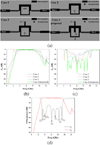
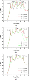
This section illustrates the structural design evolution of the proposed UWB BPF. Figure 1 depicts four configurations and their corresponding frequency responses. Initially, for better impedance matching, the stepped-impedance ring resonator (SIRR) is fed by a 50 ohm microstrip line at the ports, designated as case 1, as shown in Fig. 1 (a). It provides a wider bandwidth and a deeper attenuation zero. It resonates at 6 GHz and provides good return loss, but the 4-8 GHz passband bandwidth is narrow.
To widen the bandwidth, a short-circuit metallized hole was added to the bottom half of the SIRR, forming a short-circuit SIRR (case 2). Figure 1 (b) shows a wider bandwidth than case 1, but poor insertion loss at the passband edges. Figure 1 (c) shows multiple passband poles but poor return loss.
To adjust the passband cutoff frequencies, short- and open-circuit stubs were added to the upper half of the short-circuit SIRR. The short-circuit stub (case 3) improved the lower cutoff frequency, as shown in Figs. 1 (b) and (c). An open-circuit stub could similarly adjust the upper cutoff frequency, simplified here.
The final filter (case 4), offers a 2.8-9.5 GHz passband, a 108.9% fractional bandwidth at 6.15 GHz, and the attenuation poles are located at f = 3.2, f = 3.8, f = 4.2, f = 6.1, f = 7.2, f = 8.3, and f = 9.2. Figure 1 (d) shows excellent in-band performance.
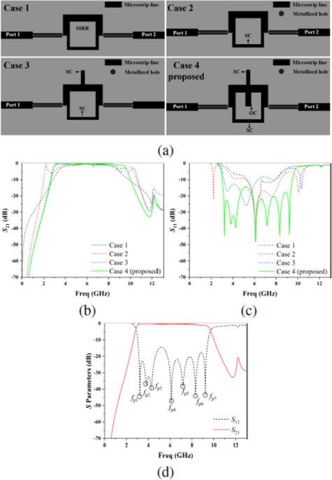
Figure 1: (a) Evolution layout of the proposed filter, (b) and (c) frequency response for different cases, (d) S-parameter response for case 4.
III. ANALYSIS OF THE PROPOSED UWB FILTER
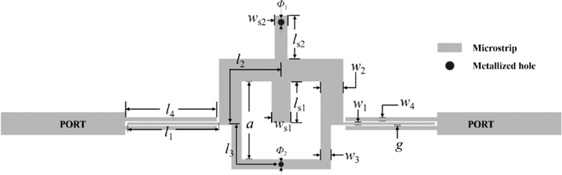
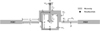
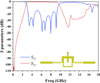
Figure 2: Architecture of the proposed UWB-BPF.
Figure 2 depicts the structure of the proposed microstrip line UWB-BPF. We introduce a new short-circuit stub-loaded stepped-impedance ring resonator that has been thoroughly analyzed. This innovative design deviates from the traditional ring resonator by integrating a short-circuit stub and an open-circuit stub above the central position of the resonator. Additionally, a metalized hole structure is loaded on the microstrip line beneath its symmetric position. The ring resonator also features a pair of coupled transmission lines on both sides for feeding, each with a length of one-quarter wavelength (/4) and admittance Y. The resonator is divided into two parts from the horizontal position of the coupled transmission lines. The upper part measures one-half wavelength (/2) and has admittance Y, while the lower part is the same half wavelength (/2) and has admittance Y.

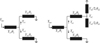
Figure 3: Equivalent circuits of the proposed resonator: (a) odd-mode equivalent circuit, (b) even-mode equivalent circuit.
The symmetry of the resonator allows us to utilize the odd- and even-mode approach to study its resonance characteristics, where the odd and even modes can be calculated in the same way as in [21]. Figure 3 illustrates the equivalent transmission line circuit for both odd and even modes. Y represents the odd-mode input admittance and Y represents the even-mode input admittance. For odd-mode excitation, the odd-mode input admittance can be expressed as
| (1) |
where
| (2) |
According to the resonance condition Y = 0, we can get
| (3) |
When the even mode is excited, the resonant modes are derived:
| (4) |
where
| (5) |
Similarly, the resonance condition Y = 0.
Using equations (1)-(5), we can explicitly determine all even- and odd-mode resonant frequencies. Equations (3) and (5) reveal that and (or l and l) solely impact the even-mode frequencies and do not affect the odd-mode frequencies.
Where = 2f = l, the electrical length ratio: / = l/l, / = l/l. According to the designed center frequency f = 6.85 GHz and the effective dielectric constant of the substrate, it is easy to determine that the value of l is /4 ( is the guided wave wavelength at the f). Therefore the physical length is chosen to be 7.4 mm. Assume here that the width of w is 0.2 mm, then Z = 127.4 . According to [22], it can be determined that the impedance values of Z and Z are 50.3 and 77.8 , respectively. In this way, we can calculate w = 1.5 mm and w = 0.8 mm.
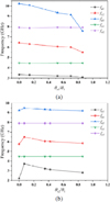
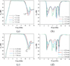
When and are equal to 0 (there are no open-circuit and short-circuit stubs), we determine the odd-mode and even-mode frequencies under weak coupling, as shown in Fig. 4. At this time, we set / = 0/7.4 (1.1/7.4, 2.2/7.4, 3.3/7.4). In Fig. 4 (a), the even-mode frequencies (f, f, f) decrease from high to low frequencies as the electrical length ratio / shifts from 0 to 0.86. f and f experience the sharpest drop.
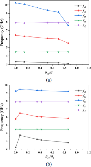
Figure 4: (a) Even- and odd-mode frequencies (f, f, f, f, f) under variation of ; (b) even- and odd-mode frequencies (f, f, f, f, f) under variation of .
When / changes from 0/7.4 to 0.9, and it is observed that the even-mode frequencies (f, f, f) are significantly lower at an electrical length ratio / of 0 than at 0.1. Between electrical length ratio / of 0.1 to 0.9, the three even-mode frequencies transition gradually to lower frequencies. According to Fig. 4, we choose / equal to 0.44 and / equal to 0.47. So we can get l = 3.3 mm and l = 3.5 mm. While keeping l and l unchanged, by increasing the stub width, it is found that when Z = 56 and Z = 69.8 , the five resonant frequencies have a good frequency distribution.
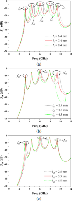
Figure 5: Simulated response of the proposed resonator under weak coupling: (a) l length variation, (b) l length variation, (c) l length variation.
After analyzing the five resonant frequencies, we can further achieve the required passband by varying the length of each stub of the proposed resonator. Figure 5 (a) depicts the variation of the five odd-even mode frequencies with the length l, indicating that l has an effect on both odd- and even-mode frequencies. Furthermore, we studied the impact of l and l on the even-mode frequencies in the passband, as shown in Figs. 5 (b) and (c). We found that l has a greater effect on the even-mode frequency f, whereas l has a greater effect on the even-mode frequency f. By tuning these two parameters, we can expand the frequency range to meet the UWB passband requirements. The five frequencies of the resonator are 3.24 GHz, 4.42 GHz, 6 GHz, 7.86 GHz, and 9.45 GHz. Hence, the first five resonant frequencies can be assigned over a broad range, making it advantageous for UWB filter design. According to the above analysis, the optimal value of the short-circuit SIRR here is as follows: l = 8.5, Z = 51 , l = 6.78, Z = 78.2 , l = 3.3, Z = 56.5 , l = 3.5, Z = 70.2 . To achieve the necessary frequency range for UWB, the interdigital-coupled lines structure has been utilized. This structure effectively shifts the attenuation zero of the lower stopband, resulting in a tighter coupling. However, the current manufacturing methods present a limitation on the coupling strength. The minimum coupling gap that can be achieved is only 0.1 mm.
After conducting the aforementioned analysis, we have successfully optimized the fundamental structure of the filter. The simulation S-parameters of the UWB bandpass filter are illustrated in Fig. 6. Considering factors such as impedance matching and reflection effects, the passband of 2.8-9.5 GHz is finally selected. An additional pole in the passband may be due to the strong coupling of the interdigital-coupled lines. It is worth noting that there exists a transmission zero at both the lower and upper passband edges, specifically located at 0.2 GHz and 11.74 GHz, respectively. Moreover, the insertion loss and return loss are both better than 0.5 and 14.3 dB, respectively, in the passband. Furthermore, additional transmission zeros present in the upper stopband contribute to extending the stopband to 16 GHz.
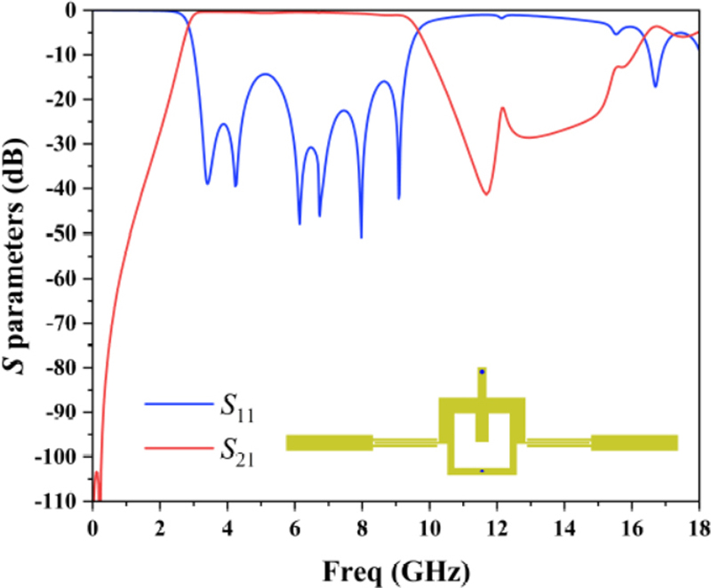
Figure 6: Simulated response of the basic UWB filter for the range 0-17 GHz.
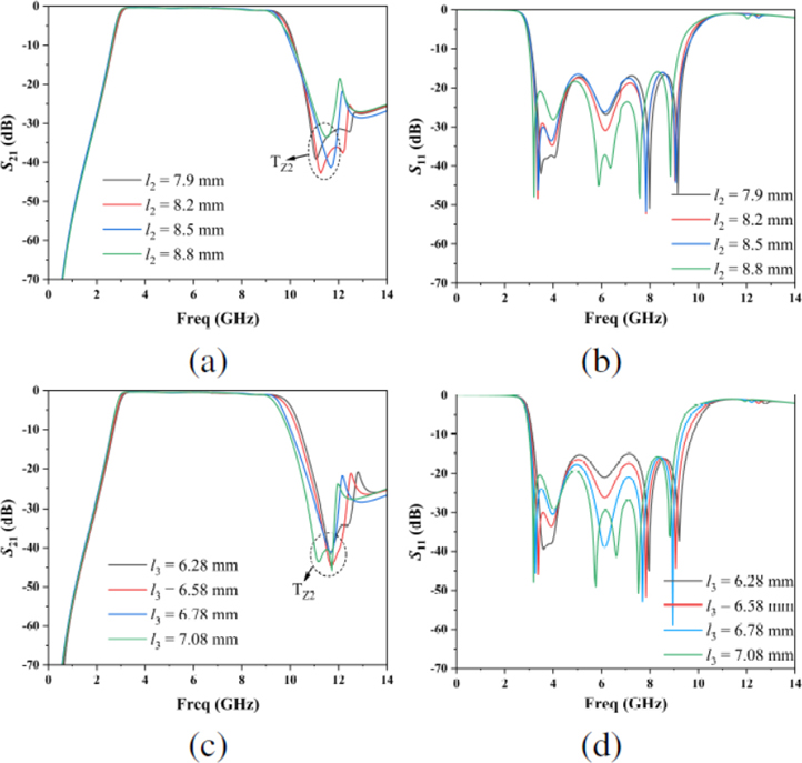
Figure 7: Filter frequency response S-parameters: (a) and (b) variation of l, (c) and (d) variation of l.
As demonstrated in Figs. 7 (a-d), we may also modify additional parameters (l and l) to improve the frequency characteristics of the filter. The location of the transmission zero on the passband’s edge and the passband return loss are both impacted by the length of the stepped impedance ring short-circuit resonator. Changing the lengths of l and l will move the transmission zeros, as seen in Figs. 7 (a) and (c), which will affect the passband bandwidth. The filter may adhere to the UWB spectrum restriction and provide outstanding roll-off characteristics by optimizing the lengths of both. As illustrated in Figs. 7 (b) and (d), changing the resonator length further reduces the passband insertion loss, and fine-tuning the corresponding length may further enhance in-band performance. As the passband in this instance exhibits a reflection characteristic larger than -13 dB and the passband edge transmission zero is better than the suppression of 30 dB, the ideal values utilized here are l = 8.5 mm and l = 6.78 mm. The suggested structure’s final optimal dimension values are (in millimeters): l = 7.4, w = 0.2, l = 8.5, w = 1.8, l = 6.78, w = 0.8, l = 7.4, w = 0.3, l = 3.3, w = 1.5, l = 3.5, w = 1, = 0.5, = 0.4, a = 6.3, g = 0.1.
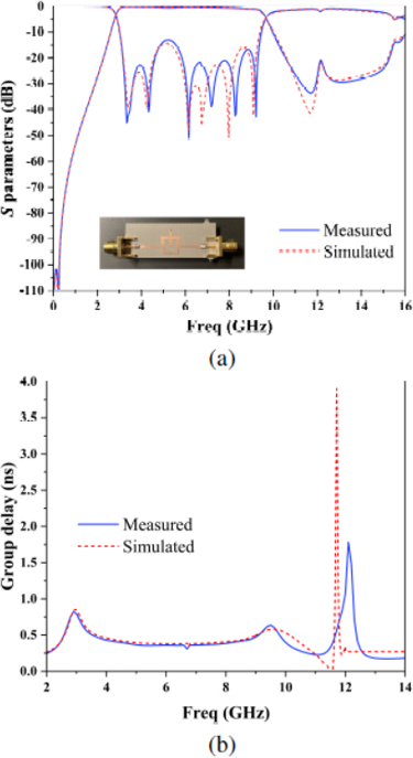
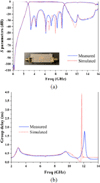
Figure 8: The measured and simulated (a) S-parameters and (b) group delays.
Table 1: Comparison of the proposed filter with other reported UWB bandpass filters
| Ref. | 3 dB FBW (%) | Stopband (GHz)/Attenuation (dB) | Size ( ) | Material |
| [4] | 95 | 14/20 | 1.240.67 | Copper |
| [9] | 110 | 18/12 | 0.80.3 | Copper |
| [10] | 110 | 20/10 | 0.740.67 | Copper |
| [16] | 109.6 | 17/17 | 0.950.78 | Copper |
| [20] | 109.4 | 27.6/20 | 0.5140.312 | Copper |
| [21] | 125.3 | 16/20 | 1.571.18 | HTS |
| This work | 108.9 | 15/20 | 0.840.41 | Copper |
IV. EXPERIMENTAL VERIFICATION
The results of testing the manufactured filter on a Vector Network Analyzer ZNB40 are shown in Fig. 8. The experimental findings are fundamentally consistent with the simulation outcomes. The passband, with a 3 dB threshold, spans from 2.8 GHz to 9.5 GHz, denoting a relative bandwidth of 108.9%. The highest level of insertion loss within the band is measured at 0.36 dB. The proposed filter exhibits an in-band return loss that exceeds 13 dB. Moreover, it demonstrates out-of-band suppression of over 110 dB at the lower stopband and attenuation greater than 20 dB at the upper stopband, which extends to approximately 15 GHz. The measured group delay, which exhibits excellent linearity, remains flat and varies from 0.38 to 0.85 ns within the passband. Discrepancies between the measured data and the simulation outcomes can be attributed to human error in fabrication and measurement, restricted substrate area, and possible connector reflections. Our ultra-wideband (UWB) bandpass filter is compared with existing examples found in the current literature, as presented in Table 1. The major benefit compared to materials of the same level is its lower insertion loss. The size has a minor benefit over different material levels.
V. CONCLUSION
A compact UWB bypass filter employing interdigital-coupled lines and a multi-stub-loaded stepped-impedance ring resonator is presented and implemented. By adjusting the corresponding stub electrical length and impedance ratio, the distribution of two odd mode frequencies and three even mode frequencies within the passband can be readily achieved. The implementation of a interdigital-coupled line as the feed for the filter is preferred due to its ability to offer optimal reflection and bandwidth. The proposed resonator possesses inherent characteristics that result in the generation of multiple transmission zeros at the upper and lower edge of the passband. This feature enhances the filter selectivity, rendering the proposed filter an attractive choice for ultra-wideband wireless communication systems.
ACKNOWLEDGMENT
This work was supported by the Research on Ultra Wideband Filters Based on Multimode Resonators under Grant China West Normal University Talent Research Fund Project 17YC054.
REFERENCES
[1] Federal Communications Commission. Revision of part 15 of the commission’s rules regarding ultra-wideband transmission systems. Tech. Rep., ET-Docket 98-153, FCC02-48, April 2002.
[2] L. Zhu, S. Sun, and R. Li, Microwave Bandpass Filters for Wideband Communications, John Wiley & Sons, pp. 116-148, Jan. 2011.
[3] J.-S. Hong and M. J. Lancaster, Microstrip Filters for RF/microwave Applications, second edition, John Wiley & Sons, pp. 123-153, 2011.
[4] C.-W. Tang and M.-G. Chen, “A microstrip ultra-wideband bandpass filter with cascaded broadband bandpass and bandstop filters,” IEEE Transactions on Microwave Theory and Techniques, vol. 55, no. 11, pp. 2412-2418, Nov. 2007.
[5] C.-L. Hsu, F.-C. Hsu, and J.-K. Kuo, “Microstrip bandpass filters for ultra-wideband (UWB) wireless communications,” IEEE MTT-S International Microwave Symposium Digest, Long Beach, CA, USA, pp. 679-682, 2005.
[6] P. P. Shome, T. Khan, S. K. Koul, and Y. M. M. Antar, “Compact UWB-to-C band reconfigurable filtenna based on elliptical monopole antenna integrated with bandpass filter for cognitive radio systems,” IET Microw. Antennas Propag., vol. 14, no. 10, pp.1079-1088, Aug. 2020.
[7] Z. Zhang and F. Xiao, “An UWB bandpass filter based on a novel type of multi-mode resonator,” IEEE Microwave and Wireless Components Letters, vol. 22, no. 10, pp. 506-508, Oct.2012.
[8] Q.-X. Chu, X.-H. Wu and X.-K. Tian, “Novel UWB bandpass filter using stub-loaded multiple-mode resonator,” IEEE Microwave and Wireless Components Letters, vol. 21, no. 8, pp. 403-405, Aug. 2011.
[9] P. P. Shome and T. Khan, “A compact design of circular ring-shaped MMR based bandpass filter for UWB applications,” IEEE Asia-Pacific Microwave Conference (APMC), Singapore, pp. 962-964, Dec. 2019.
[10] G. Saxena, P. Jain, and Y. K. Awasthi, “Design and analysis of a planar UWB bandpass filter with stopband characteristics using MMR technique,” Int. J. Micro. and Wireless Tech., vol. 13, no. 10, pp. 999-1006, 2021.
[11] G. Y. Wei, Y. X. Wang, J. Liu, Y. Gao, and X. T. Yao, “A novel highly selective UWB bandpass filter using quad-mode stub-loaded resonator,” Pro. Electromagnet. Research Lett., vol. 109, pp. 57-63, 2023.
[12] J. Liu, W. Ding, J. Chen, and A. Zhang, “New ultra-wideband filter with sharp notched band using defected ground structure,” Pro. Electromagnet. Research Lett., vol. 83, pp. 99-105, 2019.
[13] Q.-X. Chu and X.-K. Tian, “Design of UWB bandpass filter using stepped-impedance stub-loaded resonator,” IEEE Microw. and Wireless Compon.Lett., vol. 20, pp. 501-503, 2010.
[14] C. Y. Hung, M. H. Weng, and Y. K. Su., “Design of compact and sharp rejection UWB BPFs using interdigital stepped-impedance resonators,” IEICE Transactions on Electronics, vol. 90, pp. 1652-1654, 2017.
[15] X. H. Luo, X. Cheng, J. A. Han, L. Zhang, F. J. Chen, Y. J. Guo, and X. J Deng, “Compact dual-band bandpass filter using defected SRR and irregular SIR,” Electronics Letters, vol. 55, pp. 463-465, 2019.
[16] Y.-C. Chang, C.-H. Kao, M.-H. Weng, and R.-Y. Yang, “Design of the compact wideband bandpass filter with low loss, high selectivity and wide stopband,” IEEE Microw. and Wireless Compon. Lett., vol. 18, pp. 770-772, 2008.
[17] M. Sazid, N. S. Raghava, and A. N. Ghazali, “UWB-BPF based on broadside coupled technology with triple-notched passband,” Microw. Opt. Technol. Lett., vol. 65, no. 7, pp. 1910-1916, July 2023.
[18] A. N. Ghazali, M. Sazid, and B. Virdee, “A compact UWB-BPF based on microstrip-to-CPW transition with multiple transmission zeros,” Microw Opt. Technol. Lett., vol. 60, no. 8, pp. 1925-1928, Aug. 2018.
[19] C. H. Kim and K. Chang, “Ultra-wideband (UWB) ring resonator bandpass filter with a notched band,” IEEE Micro. and Wire. Compon. Lett., vol. 21, no. 4, pp. 206-208, April 2011.
[20] H. Zhu and Q.-X. Chu, “Ultra-wideband bandpass filter with a notch-band using stub-loaded ring resonator,” IEEE Micro. and Wire. Compon. Lett., vol. 23, no. 7, pp. 341-343, July 2013.
[21] Z. Long, M. Tian, T. Zhang, M. Qiao, T. Wu, and Y. Lan, “High-temperature superconducting multimode dual-ring UWB bandpass filter,” IEEE Transactions on Applied Superconductivity, vol. 30, no. 2, pp. 1-4, March 2020.
[22] C. H. Kim and K. Chang, “Ring resonator bandpass filter with switchable bandwidth using stepped-impedance stubs,” IEEE Transactions on Microwave Theory and Techniques, vol. 58, no. 12, pp. 3936-3944, Dec. 2010.
BIOGRAPHIES

Guangyong Wei was born in Chongqing. He received a bachelor’s degree in engineering. He received a bachelor’s degree in electronic information from Panzhihua University in 2021. He is currently studying for a master’s degree.
His research interests are RF microwave devices, UWB antennas.

Yunxiu Wang was born in Kaizhou, Chongqing, in 1967. In December 2008, she graduated from the School of Physics and Electronics, University of Electronic Science and Technology of China with a doctorate in science. From August 2012 to August 2013, she was a visiting scholar at Nanyang Technological University, Singapore. Current research fields mainly include electromagnetic field and microwave technology, scientific research, and teaching of microwave passive devices. She participated in 4 National Natural Science Foundation projects and 1 University Doctoral Fund project. She presided over 1 Sichuan Provincial Key Project, 1 Sichuan Provincial Scientific Research Fund Project, 1 Sichuan Provincial Department of Education Teaching Reform Project, 1 school project Doctoral start-up project, 1 school-level overseas returnee project, and 2 school-level excellent courses.

Jie Liu was born in Sichuan, China, in 1999. In 2021, he will receive a bachelor’s degree from China West Normal University. He has won several Blue Bridge Electronic Design Awards at the school. In September 2021, he will continue to study for a master’s degree at China West Normal University. He graduated from the School of Electronic Information Engineering, China West Normal University, Nanchong, China.
His main research directions include computational electromagnetics, bandpass filters, and numerical calculations.

Haiping Li was born in 1998 in Bazhong City, Sichuan Province, China. In 2021, he graduated from Panzhihua University, majoring in electronic information engineering, with a bachelor’s degree. He is currently studying for a master’s degree in optical fiber sensing at the School of Electronic Information Engineering, China West Normal University, and his current research interest is optical fiber technology.
ACES JOURNAL, Vol. 38, No. 7, 496–502
doi: 10.13052/2023.ACES.J.380705
© 2023 River Publishers