Compact Series-fed Circularly-polarized Patch Array basedon Microstrip Line
Gengming Wei, Le Chang, and Yu Wu
1School of Electronic Engineering
Xidian University, Xi’an, 710071, China
wud9032@163.com
2Global Big Data Technologies Centre
University of Technology Sydney, Ultimo, NSW 2007, Australia
wud9032@163.com
3Shaanxi Key Laboratory of Deep Space Exploration Intelligent Information Technology
School of Information and Communications Engineering, Xi’an Jiaotong University, Xi’an, 710071, China
changle4015@126.com
4Apple R&D
Beijing, 100022, China
q2770c@126.com
Submitted On: June 30, 2023; Accepted On: December 14, 2023
ABSTRACT
A compact single-layer circularly polarized (CP) antenna array is proposed in this paper for 5G/6G applications. The conventional microstrip line is modified as a feeding network by periodically and alternatively loading field blocking stubs, producing a linearly polarized in-phase radiative field aperture. By adding CP corner-truncated patches beside these in-phase fields, a linear high-gain CP antenna array excited by a single feed is obtained. The feasibility of the proposed design is demonstrated through the fabrication and measurement of a 16-element linear array. The results indicate that the 3 dB axial ratio bandwidth is 3.5% (19.6020.30 GHz), the -10 dB impedance bandwidth totally covers the 3 dB axial ratio bandwidth, and the peak realized gain is 14.9 dBi under an antenna length of 5.69. This proposed strategy provides a very compact antenna structure to achieve high-gain CP radiation without the requirement of impedance transformers, phase shifters, and open-stop-band suppressing measures. Moreover, the antenna has a per-unit-length CP gain of 5.5/, which is superior to many single-layer high-gain CPantennas.
Keywords: Circularly-polarized antenna, microstrip line, microstrip patch antenna, series-fed antenna array.
I. INTRODUCTION
Circularly-polarized (CP) planar antenna arrays are widely used in 5G/6G mobile communications and sensing systems due to their advantages of low profile, reduced polarization mismatch, and improved robustness to environmental interference [1–3]. There are two primary types of feeding approaches: parallel and series feed. Parallel-fed arrays often require a large area to accommodate multiple power dividers/combiners, resulting in a large circuit area and associated loss [1–5]. The design becomes more complex when sequential rotation method is implemented to improve axial ratio bandwidth due to the newly introduced phase shifters [5–9]. Series-fed arrays are usually constructed by cascading the basic radiators along one dimension. They possess a more compact and simple design and have lower feed loss compared to parallel-fed arrays [3]. There exist two types of series-fed arrays, including standing-wave and traveling-wave arrays. The difference lies in whether the main line connecting these radiators is with a standing or traveling wave [3]. This simple and compact design strategy makes series-fed arrays a good choice for communication and sensing applications that require high-gain planar antennas [2].
Figure 1: Radiation principle to produce CP radiation. Field distributions of (a) a microstrip line with a shorted end, (b) an end-shorted microstrip line with blocking stubs, and (c) the proposed antenna.
Several transmission lines, such as waveguides, substrate-integrated waveguides, strip lines, and microstrip lines, can be used to construct series-fed CP arrays [1–4]. Waveguide-based arrays are known for their low loss and high-power capacity, but they have bulky volume [10]. Substrate-integrated waveguide arrays are a widely used solution due to their simple fabrication process of printed circuit board technology [11–19]. Microstrip lines are more preferred when designing single-layer CP antenna arrays. They have a simple structure and are easy to integrate with microwave components and circuits [20–26].
A compact high-gain CP array faces some challenges, such as complicated design and extra power loss. The former is reflected in newly introduced impedance transformers, phase shifters, and open-stop-band (OSB) suppressing measures. The most common series-fed patch array needs to calculate and tune impedance transformers individually from the last element to the first, so multiple impedance transformers are indispensable [25]. Sometimes, phase shifters are required to guarantee all the array elements with identical excitation phase in order to produce a broadside beam [24, 25]. When a leaky-wave antenna is adopted, the OSB effect needs to be eliminated for broadside radiation, which can be realized by two main measures. One is designing reflection-canceling unit cells [11, 13, 21, 27]. Another measure is to introduce axial-asymmetrical transmission lines [28]. At the end of the leaky-wave antenna, a terminal load is added to absorb the residual power to maintain the traveling wave property [11, 13, 20, 21, 27, 28]. It will introduce extra loss, especially when the leaky-wave antenna scale is small.
In this paper, a single-layer CP patch array is presented that utilizes a specially-designed feeding network. The network is constructed by alternately and periodically loading blocking stubs on a microstrip line, which can excite a series of corner-truncated CP patches. The proposed strategy is verified through the fabrication and measurement of a 16-element CP patch array. This innovative design has several advantages: 1) It provides a compact high-gain CP antenna strategy that eliminates the need for impedance transformers, phase shifters, and OSB suppressing measures. 2) The proposed antenna achieves a relatively high per-unit-length CP gain compared to other reported single-layer high-gain CP antennas. 3) Compared to leaky-wave antennas, the proposed antenna is with reduced dissipated power loss, particularly when the array size is limited.
II. ANTENNA DESIGN
A. Radiation principle
Figure 1 (a) shows the field distribution of a microstrip line with a shorted end. It is known that an electromagnetic wave is confined and propagates within the microstrip line due to the symmetric and periodic fields along the line. The introduction of blocking stubs on the fields with the same orientation can suppress the fringing fields on one side, generating a microstrip line with fringing fields pointing in the same direction, as depicted in Fig. 1 (b), where the fields pointing to the +X direction denoted by the red arrow lines are produced, and the ones along the -X denoted by blue are suppressed. The length of the blocking stubs should be selected to be approximately a quarter wavelength to transform the shorted end generated by the metallic via to the open end at the interconnection point. In this way, the transmission mode of the microstrip line could be maintained. This concept has been applied to construct a linearly polarized aperture previously in [29]. Here, it is employed as a feeding network to generate a CP antenna array.
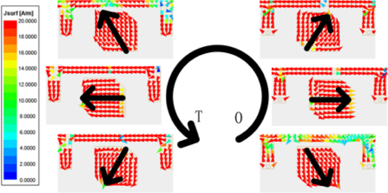
Figure 1 (c) depicts the field distribution of the proposed antenna. The high-gain CP beam is obtained by utilizing the compact feeding network to capacitively couple power to the CP patches along the microstrip line. The CP patch is created by modifying a rectangular patch with diagonal perturbations. Figure 2 shows current distributions on an arbitrarily chosen patch at 20 GHz under different phases. The current rotates in an anticlockwise direction, which follows the right-handed rule. So, right-hand circular polarization (RHCP) broadside radiation is achieved.
Figure 2: Current distributions on an arbitrarily chosen patch at 20 GHz under different phases.
B. Scalability
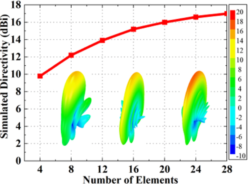
Figure 3 depicts the broadside directivities at 20 GHz as a function of element numbers. The directivity increases as the element increases, and the directivity increase trend follows a logarithmic distribution. Elements numbering 16 is a nice compromise between array size and directivity. Further increasing the elements contributes little to directivity improvement.
Figure 3: Simulated broadside directivities at 20 GHz with different element numbers.
Figure 4: Geometry of the proposed antenna. The parameters are = 2 mm, = 5 mm, = 4 mm, = 4.1 mm, = 1.2 mm, = 2.6 mm, = 0.4 mm, = 0.9 mm.
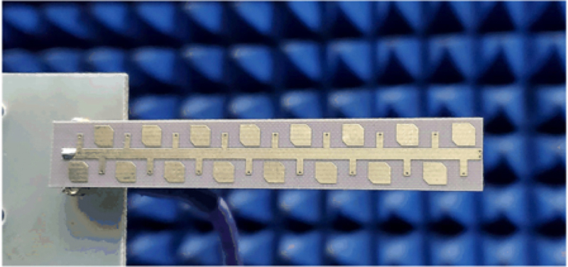
Figure 5: Fabricated prototype.
C. Antenna geometry
The geometry of the proposed antenna is presented in Fig. 4. It is a single-layer structure based on a 1.016 mm-thick TLX-8 substrate (r = 2.55, tan = 0.0019). The proposed antenna consists of a compact feeding network and 16 CP radiating patches. The feeding network is a blocking-stubs-loaded microstrip line with its rear end shorted. The microstrip line has width wl = 2 mm, and its shorted end is realized by using two vias with diameter 0.4 mm and spacing 1 mm. The blocking stubs are shorted rectangular metal slices with length ls = 2.6 mm and width ws = 1.2 mm. Their shorted ends are realized by using shorted vias with diameter 0.4 mm. The patches are located at the openings of the feeding network with a gap of dp = 0.4 mm. The corner-truncated patch chamfered with length ap = 0.9 mm achieves the RHCP radiation. These patches are with the length, width, and spacing of lp = 4.1 mm, wp = 4 mm, and ds = 5 mm, respectively.
The input port locates at the bottom surface, as shown in the enlarged inset on the bottom-left corner of Fig. 4. The feeding probe is a metallic via hole with a diameter of 0.6 mm, which is situated at the center of a metal ring with a width of 0.3 mm. The circular ring with a width of 1.4 mm, marked by red, is where the lumped port is located.
III. VALIDATION AND PERFORMANCE COMPARISON
A. Fabrication and measurement
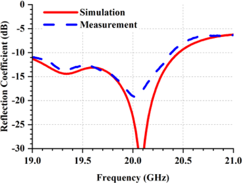
Figure 6: Simulated and measured reflection coefficients.
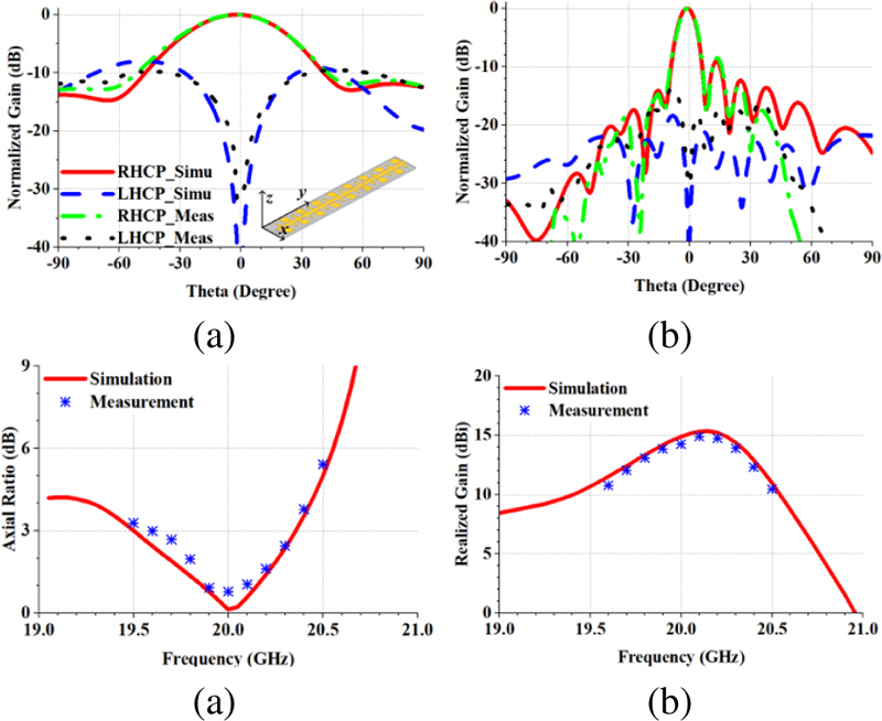
Figure 7: Simulated and measured results of the (a) normalized radiation pattern in XOZ plane at 20 GHz, (b) normalized radiation pattern in YOZ plane at 20 GHz, (c) axial ratio, and (d) realized gain.
Table 1: Performance comparison between the proposed antenna and other recently reported single-layer series-fed CP arrays
| Refs. | Array Scale | Antenna Length | Freq. | Peak Gain | CP Gain Per Unit Length | No Impedance Transformers? | No Phase Shifters? | No Need to Suppress OSB? |
| [11] | 14.41 | 17.00 | 17.0 | 3.5 | ||||
| [13] | 15.20 | 16.00 | 18.9 | 5.1 | ||||
| [19] | 4.10 | 6.65 | 10.3 | 2.6 | ||||
| [21] | 5.83 | 7.82 | 12.5 | 3.1 | ||||
| [24] | 4.28 | 7.14 | 16.3 | 10.0 | ||||
| [25] | 2.25 | 2.37 | 10.0 | 4.4 | ||||
| [26] | 4.24 | 3.00 | 16.0 | 9.4 | ||||
| This Work | 5.69 | 20.10 | 14.9 | 5.5 |
The proposed antenna is manufactured using standard printed circuit board technology. The fabricated prototype is depicted in Fig. 5. The S parameter of the developed array was measured using a Keysight N5244B PNA-X Microwave Network Analyzer. The radiation pattern was measured with a NSI2000 antenna measurement system. The simulated and measured results are shown in Figs. 6 and 7. They agree very well. The simulated and measured reflection coefficients are depicted in Fig. 6. The measured -10 dB impedance bandwidth exceeds 4.4% (19.5020.38 GHz), while the simulated exceeds 4.8% (19.5020.45 GHz). Acceptable impedance bandwidth is obtained. Simulated and measured normalized radiation patterns at 20 GHz in two principal planes (XOZ and YOZ) are shown in Figs. 7 (a) and (b). A fan-shaped beam for co-polarization (RHCP) is observed. It is with a wide 2-D pattern in the XOZ plane, a narrow beam in the YOZ plane. The results exhibit excellent RHCP performance with good cross-polarization discrimination (XPD). In the broadside direction, the measured XPD is 30.7 dB, while the simulated exceeds 40.0 dB. In the upper space, the measured XPDs of both planes are superior to 9.5 dB, while the simulated are better than 8.0 dB. Figures 7 (c) and (d) show the axial ratio and realized gain at broadside. The measured 3 dB axial ratio bandwidth is 3.5% (19.6020.30 GHz), while the simulated is 4.3% (19.5020.35 GHz). The measured peak gain is 14.9 dBi, while the simulated is 15.4 dBi, both appearing at 20.10 GHz.
B. Performance comparison
The performance comparison between the proposed antenna and other recently reported single-layer series-fed CP arrays is presented in Table 1. As seen from the table, the proposed antenna exhibits two significantmerits.
Firstly, the proposed antenna offers a compact design strategy for achieving a high-gain patch array. The existing strategies either need impedance transformers [13, 19, 24–26], phase shifters [24, 25], or extra OSB suppressing designs [11, 13]. In contrast, the proposed antenna is so compact that all three factors are unnecessary.
Secondly, the proposed antenna exhibits a high per-unit-length gain (refers to the absolute gain value produced by unit length). It is with the per-unit-length realized gain of 5.5/, which is higher than 5 of the 7 references [11, 13, 19, 21, 25].
In addition, the proposed antenna is a standing-wave antenna compared to leaky-wave antennas. It is with a shorted end rather than a terminal load, so the proposed strategy is especially beneficial to design a small-scale patch array [11, 13, 21]. In contrast, the small-scale leaky-wave antenna suffers from dissipated power absorbed by the terminal load.
IV. CONCLUSION
This paper proposes a compact strategy to produce a single-layer high-gain CP antenna array. By introducing blocking stubs periodically and alternatively on a one-end-shorted microstrip line, a design-friendly feeding network is obtained. By adding CP corner-truncated patches beside these in-phase fields, a linear high-gain CP antenna array excited by a single feed is obtained. A fabricated prototype has demonstrated its feasibility. The design is so simple because it eliminates the requirement of impedance transformers, phase shifters, and additional OSB suppressing measures.
REFERENCES
[1] Y. T. Lo and S. W. Lee, Antenna Handbook. New York: Van Nostrand Reinhold, pp. 21-23, 1993.
[2] S. Gao, Q. Luo, and F. Zhu, Circularly Polarized Antennas. John Wiley & Sons, pp. 191-258, 2014.
[3] J. R. James and P. S. Hall, Handbook of Microstrip Antennas (IEE Electromagnetic Waves Series; 28), London, U.K: P. Peregrinus on behalf of the Institution of Electrical Engineers, pp. 219-272,1989.
[4] D. M. Pozar, Microwave Engineering, 4th ed., Hoboken, NJ: Wiley, pp. 95-158, 2012.
[5] J. Huang, “A technique for an array to generate circular polarization with linearly polarized elements,” IEEE Trans. Antennas Propag., vol. 34, no. 9, pp. 1113-1124, Sep. 1986.
[6] Y. Li, Z. Zhang, and Z. Feng, “A sequential-phase feed using a circularly polarized shorted loop structure,” IEEE Trans. Antennas Propag., vol. 61, no. 3, pp. 1443-1447, Mar. 2013.
[7] C. Deng, Y. Li, Z. Zhang, and Z. Feng, “A wideband sequential-phase fed circularly polarized patch array,” IEEE Trans. Antennas Propag., vol. 62, no. 7, pp. 3890-3893, July 2014.
[8] S. X. Ta and I. Park, “Compact wideband circularly polarized patch antenna array using metasurface,” IEEE Antennas Wireless Propag. Lett., vol. 16, pp. 1932-1936, Mar. 2017.
[9] A. R. Weily and Y. J. Guo, “Circularly polarized ellipse-loaded circular slot array for millimeter-wave WPAN applications,” IEEE Trans. Antennas Propag., vol. 57, no. 10, pp. 2862-2870, Oct. 2009.
[10] G. Montisci, “Design of circularly polarized waveguide slot linear arrays,” IEEE Trans. Antennas Propag., vol. 54, no. 10, pp. 3025-3029, Oct. 2006.
[11] P. Sanchez-Olivares and J. L. Masa-Campos, “Novel four cross slot radiator with tuning vias for circularly polarized SIW linear array,” IEEE Trans. Antennas Propag., vol. 62, no. 4, pp. 2271-2275, Apr. 2014.
[12] C. Zhijun, W. Hong, K. Zhenqi, C. Jixin, and K. Wu, “Circularly polarized slot array antenna based on substrate integrated waveguide,” 2008 Int. Conf. on Microwave and Millimeter Wave Technology, Apr. 2008.
[13] P. Chen, W. Hong, Z. Kuai, and J. F. Xu, “A substrate integrated waveguide circular polarized slot radiator and its linear array,” IEEE Antennas Wireless Propag. Lett., vol. 8, pp. 120-123, Apr. 2009.
[14] J. Zhu, S. Liao, Y. Yang, S. Li, and Q. Xue, “60 GHz dual-circularly polarized planar aperture antenna and array,” IEEE Trans. Antennas Propag., vol. 66, no. 2, pp. 1014-1019, Feb. 2018.
[15] H. Zhou and W. Hong, “Compact circularly polarized patch array antenna,” IEEE Antennas Wireless Propag. Lett., vol. 15, pp. 778-781, Aug. 2016.
[16] Y. Li, Z. N. Chen, X. Qing, Z. Zhang, J. Xu, and Z. Feng, “Axial ratio bandwidth enhancement of 60-GHz substrate integrated waveguide-fed circularly polarized LTCC antenna array,” IEEE Trans. Antennas Propag., vol. 60, no. 10, pp. 4619-4626, Oct. 2012.
[17] J. Huang, W. Lin, F. Qiu, C. Jiang, D. Lei, and Y. J. Guo, “A low profile, ultra-lightweight, high efficient circularly-polarized antenna array for Ku band satellite applications,” IEEE Access, vol. 5, pp. 18356-18365, Sep. 2017.
[18] D. F. Guan, C. Ding, Z. P. Qian, Y. S. Zhang, Y. J. Guo, and K. Gong, “Broadband high-gain SIW cavity-backed circular-polarized array antenna,” IEEE Trans. Antennas Propag., vol. 64, no. 4, pp. 1493-1497, Apr. 2016.
[19] Z. Hao, X. Liu, X. Huo, and K. Fan, “Planar high-gain circularly polarized element antenna for array applications,” IEEE Trans. Antennas Propag., vol. 63, no. 5, pp. 1937–1948, May 2015.
[20] S. Ogurtsov and S. Koziel, “A conformal circularly polarized series-fed microstrip antenna array design,” IEEE Trans. Antennas Propag., vol. 68, no. 2, pp. 873-881, Feb. 2020.
[21] T. R. Cameron, A. T. Sutinjo, and M. Okoniewski, “A circularly polarized broadside radiating “herringbone” array design with the leaky-wave approach,” IEEE Antennas Wireless Propag. Lett., vol. 9, pp. 826-829, Aug. 2010.
[22] S. J. Chen, C. Fumeaux, Y. Monnai, and W. Withayachumnankul, “Dual circularly polarized series-fed microstrip patch array with coplanar proximity coupling,” IEEE Antennas Wireless Propag. Lett., vol. 16, pp. 1500-1503, Jan. 2017.
[23] N. Nguyen-Trong, S. J. Chen, and C. Fumeaux, “High-gain dual-band dual-sense circularly polarized spiral series-fed patch antenna,” IEEE Open Journal of Antennas and Propagation, vol. 3, pp. 343-352, Mar. 2022.
[24] Q. Chen, Y. Wei, J. Zhang, and W. Wu, “Dual-band circularly polarized shared-aperture array with wideband and small frequency ratio,” 2016 IEEE Int. Conf. on Ubiquitous Wireless Broadband, pp. 1-3, Oct. 2016.
[25] P. D. Hilario Re, D. Comite, and S. K. Podilchak, “Single-layer series-fed planar array with controlled aperture distribution for circularly polarized radiation,” IEEE Trans. Antennas Propag., vol. 68, no. 6, pp. 4973-4978, June 2020.
[26] K. Hirose, K. Shinozaki, and H. Nakano, “A comb-line antenna modified for wideband circular polarization,” IEEE Antennas Wireless Propag. Lett., vol. 14, pp. 1113-1116, May 2015.
[27] H. Lee, J. H. Choi, C.-T. M. Wu, and T. Itoh, “A compact single radiator CRLH-inspired circularly polarized leaky-wave antenna based on substrate-integrated waveguide,” IEEE Trans. Antennas Propag., vol. 63, no. 10, pp. 4566-4572, Oct.2015.
[28] S. Otto, Z. Chen, A. Al-Bassam, A. Rennings, K. Solbach, and C. Caloz, “Circular polarization of periodic leaky-wave antennas with axial asymmetry: theoretical proof and experimental demonstration,” in IEEE Trans. Antennas Propag., vol. 62, no. 4, pp. 1817-1829, Apr. 2014.
[29] L. Chang, Z. Zhang, Y. Li, and M. F. Iskander, “Single-layer magnetic current antenna array with high realized aperture usage rate based on microstrip line structure,” IEEE Trans. Antennas Propag., vol. 65, no. 2, pp. 584-592, Dec. 2017.
BIOGRAPHIES

Gengming Wei received the B.S. degree from Xidian University, Xi’an, China, in 2012. He is currently pursuing the collaborative Ph.D. degree between Xidian University and the University of Technology Sydney, Sydney, NSW, Australia. His research interests include UWB antennas, high-gain antennas with low profile, wireless power transfer systems, and antenna measurement systems.

Le Chang received the B.S. degree in electronics and information engineering from Xidian University, Xi’an, China, in 2012, and the Ph.D. degree in electrical engineering from Tsinghua University, Beijing, China, in 2017. In July 2017, he joined Huawei Technology Ltd., Beijing, China, as a senior antenna engineer. Since 2021, he has been with Xi’an Jiaotong University, where he is currently an associate professor. He has authored or co-authored over 34 journal articles. His current research interests include mobile antennas and mmW/THzantennas.

Yu Wu received the M.S. degree in electronics and information engineering from Xidian University, Xi’an, China, in 2016.
He is currently a senior engineer with Apple R&D, Beijing, China. His current research interests include mobile antennas, mobile device signal measurements in all kinds of scenarios.
ACES JOURNAL, Vol. 38, No. 10, 761–766
doi: 10.13052/2023.ACES.J.381002
© 2023 River Publishers

