A Low-power, High-gain and Excellent Noise Figure GaN-on-SiC LNA Monolithic Microwave Integrated Circuit (MMIC) operating at Ka-band for 5G/6G Application
Zhou Dai, Chunyu Li, Junda Yan, Tiancheng Zhang, and Huaguang Bao
1School of Microelectronics (School of Integrated Circuits)
Nanjing University of Science and Technology, Nanjing, China
2Nanjing Electronic Devices Institute
Nanjing, China
daizhou1986@163.com
Submitted On: July 5, 2023; Accepted On: October 22, 2023
ABSTRACT
A 25-40 GHz monolithic low-noise amplifier (LNA) is designed and fabricated with the 100 nm gallium nitride on silicon carbide (GaN-on-SiC) technology. This four-stage-cascade monolithic LNA performs a low DC power consumption of 150 mW and noise figure of 1.6-2.2 dB. Moreover, the gain of 34-37 dB with the continuous wave of more than 2 W over 24 hours can be achieved covering the operating bandwidth. Hence, this state-of-art LNA possesses a great potential to be directly integrated with GaN power amplifiers and other microwave components to realize the high-integration, high-reliability, and high-power RF front-end.
Keywords: Gallium nitride on silicon carbide (GaN-on-SiC), high gain, low-noise amplifier (LNA), low DC power consumption, optimal noise figure.
I. INTRODUCTION
To deal with the serious loss and high packaging cost of the transmitter and receiver millimeter-wave (mm-Wave) front-end, monolithic microwave integrated circuit (MMIC) technique is extended to the mm-Wave frequency range and is fabricated the components on the same chip [1]. GaN material has the advantages of wide band gap and high electron mobility [2], such that a GaN low-noise amplifier (LNA) can achieve more superior breakdown resistance and higher frequency characteristics than GaAs devices. Recently, several GaN LNAs operating at Ka-band have been recorded [1, 3–6]. Depending on the substrate material, GaN LNAs are mainly classified into two types, one with GaN-on-Si process [1, 3, 4] and the other with GaN-on-SiC process [5–7]. The study of discrete components on Si substrate has been mature, leading to the conclusion that the GaN LNA with SiC substrate is not completely superior in terms of performance compared to the GaN LNA with Si substrate. The SiC substrate with high thermal conductivity allows for efficient dissipative power density, and no leakage problem as with Si substrate, which further guarantees the robustness of GaN LNA [6–7]. Moreover, with the requirement of high speed, high power, and high detection accuracy for RF front-ends, it is imperative to develop GaN LNA with wider bandwidth, lower noise, and lower power consumption.
In this work, a self-developed 0.1 m T-Gate high electron mobility transistor with ultra-thin barrier is adopted to fabricate a 25-40 GHz wideband GaN-on-SiC LNA. The GaN LNA demonstrates a high gain of 34-37 dB, an excellent DC power consumption of 150 mW, and low noise figure (NF) of 1.6-2.2 dB, simultaneously, which enables unparalleled performances in Ka-band.
II. LNA DESIGN
In this section, the process of GaN HEMT and the design of the GaN LNA MMIC is described in detail.
A. GaN HEMT
The GaN high-electron-mobility transistors (HEMTs) are prepared with a self-developed ultra-thin barrier. The AlN/GaN/AlGaN double heterojunction epitaxy structure is grown on SiC substrate by metalorganic chemical vapor deposition (MOCVD) [8]. Due to the strong polarization effect of AlN, the energy band difference of AlN/GaN is large, so a high concentration of two-dimensional electron gas (2-DEG) can be formed at the interface of the two materials [9–12]. The negative polarization charge on the back of AlN increases the energy band of the AlGaN barrier, so that the probability of 2-DEG entering AlGaN is greatly reduced. In this way, the disorder scattering in the alloy is reduced, the mobility of the 2-DEG is increased, and the device noise is improved. The Hall test shows that the heterojunction material has a 2-DEG concentration of 1.11013 cm and mobility of up to . A 100 nm T-gate with low parasitic impedance is fabricated using ion beam direct writing in combination with ultrathin gate dielectric passivation. Schottky contacts play a decisive role in device reliability and performance. In order to improve the Schottky barrier, reduce the gate leakage current, and improve the noise properties of the device, a high-barrier Ni-gate structure is used. The stability of the Schottky contact is improved by a high-temperature thermal treatment.
B. LNA
LNA is designed with four-stage-cascade amplifiers and self-biased negative feedback structure. The total NF of LNA can be written as [13]
| (1) |
where F, F, F, F, and G, G, G are NF of level 1 to level 4 and the gain of level 1 to level 3, respectively. It is obviously that the NF of the first-stage amplifier has the largest effect on the overall noise. Hence, the input impedance is matched to the optimal noise source impedance so that the NF can be effectively controlled. However, this operation may result in the risk of the impedance point deviating from the maximum gain matching position. Therefore, for compromise, M-factor is introduced as [14]
| (2) |
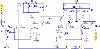
The compromise between the NF and the gain point is chosen when the M-factor reaches its minimum. Based on the above principles, a four-stage-cascaded LNA MMIC with the GaN HEMT in each stage is designed as exhibited in Fig. 1.
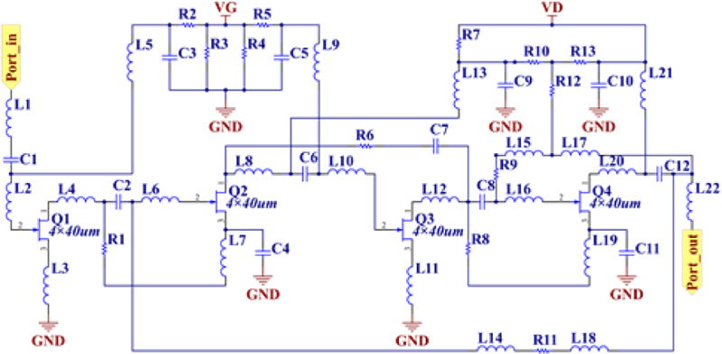
Figure 1: Schematic of the proposed LNA.
To further improve the gain flatness and robustness of the LNA, a negative feedback structure is used in the circuit design, which reduces the sensitivity of the process and increases the operating bandwidth. The resistance on the feed network is to suppress low-frequency oscillations and ensure the stability of the RF signal. The DC feed circuit at each stage is grounded through the metal-insulator-metal capacitor. To prevent AC signal leakage, a choke inductor is added between the power and HEMT and can be determined by
| (3) |
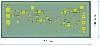
where f is the central frequency and Z is the impedance. The DC power consumption is reduced by the multiplexing current. In this way, the leakage voltage of the tube core will be significantly decreased. Thus, the layout design is completed according to the schematic diagram with the chip size of 2.20.880.05 mm. The scanning electron microscopy (SEM) graph of LNA is exhibited in Fig. 2.
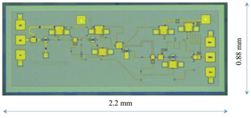
Figure 2: SEM picture of the fabricated LNA.
III. MEASUREMENTS AND DISCUSSION
A. Performances of GaN HEMT
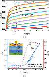
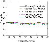
The measurement of the GaN HEMT is tested at ambient temperature (25) with a Shiel Environment TS200-SE probe station and a Keysight PNA-X N5245A vector network analyzer. Figure 3 (a) exhibits the I-V characteristics of the 440 m GaN HEMT with the gate voltage changing from -0.9 to 0 V, whose amplitude increment is 0.1 V. As can be seen from the curves, the knee voltage of the designed GaN HEMT is 1.5 V. Thus, these characteristics can achieve a lower noise coefficient and realize the current multiplexing at optimized supply voltages. Moreover, the transfer properties of the GaN HEMT are shown in Fig. 3 (b) with the maximum transconductance of 750 ms/mm, which benefits from the ultra-thin AlN barrier layer structure with strong polarization effects. The gain of the HEMT also reaches up to 10 dB at 40 GHz, as demonstrated in Fig. 4. Furthermore, the self-developed GaN HEMTs exhibit better performances than the GaAs HEMTs with the E-pHEMT process in the noise figure, which is maintained around 1.0 dB, shown in Fig. 5. Hence, this GaN HEMT can be used in the design of advanced LNA.
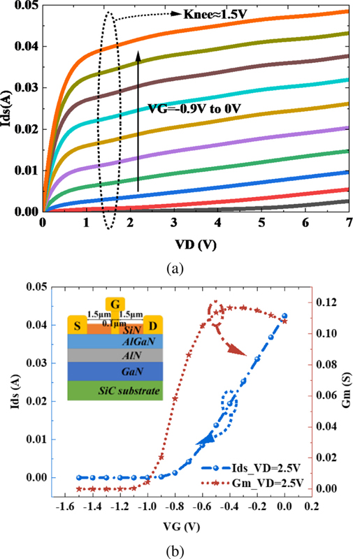
Figure 3: Output characteristics of the GaN HEMT in the proposed LNA.
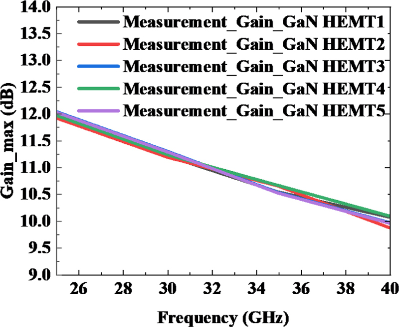
Figure 4: Comparisons of gain characteristics for the proposed GaN LNA at different HEMT cores.
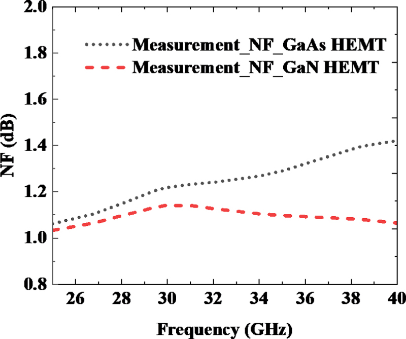
Figure 5: Superior noise figure of the proposed GaN HEMT.
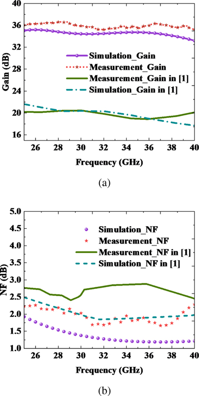
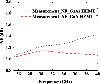
Figure 6: Comparison of the performance of the proposed LNA: (a) The gain performance of the device and (b) the noise figure of the device.
B. Properties of the GaN LNA
The simulations are performed according to the layout of the GaN LNA with input power of 2 W. The test conditions are in agreement with the simulation conditions. Figure 6 demonstrates the comparison between simulations and measurements. It can be seen that the on-chip measurement of S is in great agreement with the simulation curve in the 25-40 GHz band. Remarkably, the proposed GaN LNA achieves a high gain of 35 dB, which is a distinct advantage over other reported LNAs. Furthermore, by comparing the NF in the broadband band with the reported result in [1], the NF is reduced more than 0.5 dB, which is one of the advantages of the LNA designed in this paper. To further demonstrate the properties of the GaN LNA in high-power scenario, the attack limit of the GaN LNA is measured. As shown in Fig. 7, the proposed GaN LNA MMIC can withstand high power continuous waves up to 2 W for a long period of time without degradation in performance over the entire range of operating frequencies. As the input power increases, the performance of the LNA decreases and the working time increases. Compared to the LNA based on InP and GaAs [8], the GaN LNA exhibits better reliability under high-power conditions. This is mainly due to the outstanding thermal conductivity of the SiC substrate and the excellent high-power nature of the GaN material.
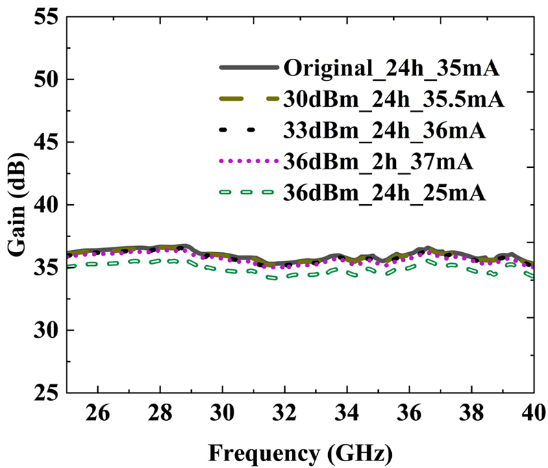
Figure 7: Attack limit of the GaN LNA.
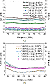
C. Consistency test at different bias voltages
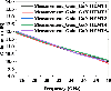
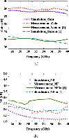
To demonstrate the excellent consistency, the performance of the GaN LNA is measured with different bias voltages. Meanwhile, the experiment is carried out at an ambient temperature of 25. A constant voltage of 5 V is applied in the drain and the gate voltage is swept from -0.3 V to -0.6 V at intervals of 0.1 V. The corresponding measured DC current is 52 mA, 41 mA, 31 mA, and 21 mA, respectively. The DC power consumption can be calculated as 0.15 W under typical operating conditions with a gate voltage of -0.5 V. This power consumption is extremely prominent for GaN LNA, which mainly benefits from the current multiplexing structure that enables GaN HEMTs to share the input power in series. This fabrication makes GaN LNA more competitive for applications in missile, airborne or space-bornecircuits.
As can be seen in Fig. 8, the trends of the gain characteristics, NF and VSWR are essentially the same when different voltage values are applied to the gate. When VG is -0.6 V, the gain features and noise coefficients are more discrete. This is because the limited current density of the core is not sufficient to support marvelous amplification and noise properties. The VSWRs of the input port and the output port are consistent across the entire frequency band. As can be seen from Fig. 8 (b), the standing-wave properties do not become discrete with the difference of gate voltages.
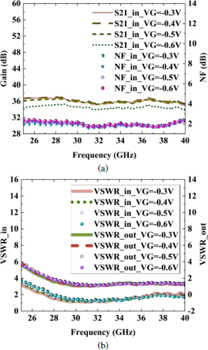
Figure 8: Comparisons of (a) gain and NF and (b) VSWRs for the proposed GaN LNA at different bias voltages.
The variation trend of VSWR with frequency is the same for different gate voltages. This is mainly to optimize the gate width, gate spacing, and lead placement of the device during the layout design of the GaN LNA to obtain better gate resistance, gate capacitance, source resistance, and source inductance.
D. High and low temperature performance
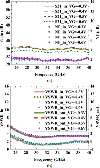
In this section, the electrical properties of the GaN LNA are measured at high and low temperatures to assess the operating conditions in harsh environments. The reliability of the GaN LNA is verified at different temperatures with the input power of 2 W, drain and gate voltages of 5 V and -0.5 V. The measured parameters are demonstrated in Fig. 9.
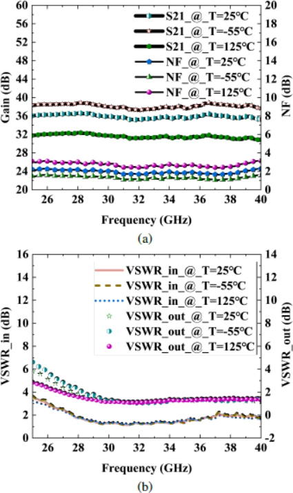
Figure 9: Comparisons of (a) gain and NF and (b) VSWRs for the proposed GaN LNA at different temperatures.
Throughout the operating band, the gain of the GaN LNA decreases with increasing temperature. This is because the carrier mobility decreases with increasing temperature, leading to a reduction in the transconductance and a worsening of the gain. As can be seen from Fig. 9 (a), the NF of the LNA presents an opposite trend to the gain as a function of temperature, which is mainly due to the enhanced thermal vibration of the lattice and the scattering effect. Moreover, the VSWRs of the input port and output ports vary slightly with temperature in the intermediate and high-frequency bands, while the dispersion is larger in the low-frequency band, as shown in Fig. 9 (b). This is caused by the fact that the temperature variability properties change the parasitic parameters and further affect the low-frequency properties.
F. Comparisons with other reported Ka-band GaN LNAs
Some performances of the proposed GaN LNA are listed in Table 1 and compared with some previously reported representative advanced GaN LNAs, including the gain, noise figure, frequency band, DC power consumption, process, and chip core area. To our surprise, the designed GaN LNA monolithic microwave integrated circuit in this work not only realized a gain of 34-37 dB in the Ka-band, which is the highest value compared to other reported works, but also simultaneously possesses a low noise behavior of 1.6-2.2 dB. In addition, the desired DC power consumption of proposed GaN LNA MMIC in this work is as low as 0.15 W. [16] reports a lower DC power consumption, but it performs poorly in other aspects such as bandwidth, gain, and noise. These performances show that the proposed GaN LNA MMIC is a competitive component in millimeter-wave front ends.
Table 1: Performance comparisons of the GaN LNA
| Ref. | Gain (dB) | NF (dB) | Frequency Band (GHz) | DC Power (W) | Process | Chip Core Area (:m) |
| [1] | 16-21.5 | 2.2-4.4 | 18-56 | 1.4 | 0.1 :m GaN/Si | 4*50 |
| [3] | 25-27 | 1.7-2.2 | 33-38 | - | 0.1 :m GaN/Si | 6*30/8*40/8*50 |
| [4] | 19.5-20.5 | 1.8-2 | 27-31 | 0.15 | 0.1 :m GaN/Si | 4*20 |
| [6] | 10-20 | 1.5-8 | 0.1-45 | 5.2 | 0.15 :m GaN/SiC | - |
| [7] | 21-25 | 2.4-2.9 | 25-31 | 0.3 | 0.15 :m GaN/SiC | 4*25 |
| [15] | 23-27 | 1.3-2.7 | Full Ka-band | 0.433 | 0.1 :m GaN/Si | - |
| [16] | 11-18 | 1.8-2.5 | 30-39.3 | 0.124 | T4-A | 4*20 |
| [17] | 20.2-24 | 2.42-2.56 | 26-30 | 0.32 | 0.15 :m GaN/SiC | - |
| [18] | 19.5-22.5 | 0.4-1.1 | 22-30 | 0.21 | 0.1 :m GaN/Si | 4*50 |
| This work | 34-37 | 1.6-2.2 | 25-40 | 0.15 | 0.1 :m GaN/SiC | 4*40 |
IV. CONCLUSION
A state-of-the-art 25-40 GHz GaN-on-SiC LNA MMIC is presented in this paper. The LNA demonstrates superior broadband performance by implementing a four-stage-cascade structure using the MOCVD process, current multiplexing scheme, and source impedance matching. Covering the entire operating frequency band, the GaN LNA demonstrates a low NF of 1.6-2.2 dB, an excellent DC power consumption of 0.15 W, a high reliability in harsh temperature scenarios, and a superior gain of 34-37 dB, offering unparalleled applications to directly integrated with GaN PA and switch to realize miniaturized, high-power, and reliable MMW front-end module.
ACKNOWLEDGMENT
This work was supported in part by National Natural Science Foundation of China Grant 62201257, 62001231, 62025109, Primary Research & Development Plan of Jiangsu Province BE2022070, BE2022070-1, Jiangsu Province Natural Science Foundation under Grant BK20200467, Jiangsu Funding Program for Excellent Postdoctoral Talent and Postgraduate Research & Practice Innovation Program of Jiangsu Province KYCX22_0438.
REFERENCES
[1] X. Tong, L. Zhang, P. Zheng, S. Zhang, J. Xu, and R. Wang, “An 18–56 GHz wideband GaN low-noise amplifier with 2.2–4.4-dB noise figure,” IEEE Microw. Wireless Compon. Lett., vol. 30, no. 12, pp. 1153-1156, Dec. 2020.
[2] R. S. Pengelly, S. M. Wood, J. W. Milligan, S. T. Sheppard, and W. L. Pribble, “A review of GaN on SiC high electron-mobility power transistors and MMICs,” IEEE Trans. Microw. Theory Techn., vol. 60, no. 6, pp. 1764-1783, Feb. 2012.
[3] C. Florian, P. A. Traverso, and A. Santarelli, “A Ka-Band MMIC LNA in GaN-on-Si 100-nm technology for high dynamic range radar receivers,” IEEE Microw. Wireless Compon. Lett., vol. 31, no. 2, pp. 161-164, Jan. 2021.
[4] L. Pace, P. E. Longhi, W. Ciccognani, S. Colangeli, F. Vitulli, F. Deborgies, and E Limiti, “DC power-optimized Ka-Band GaN-on-Si low-noise amplifier with 1.5 Db noise figure,” IEEE Microw. Wireless Compon. Lett., vol. 32, no. 6, pp. 555-558, Jan. 2022.
[5] K. W. Kobayashi, V. Kumar, C. Campbell, S. Chen, and Y. Cao, “18-44GHz K/Ka-band robust-35.5 dBm reconfigurable 90nm GaN HEMT LNA,” in 2020 IEEE BiCMOS and Compound Semiconductor Integrated Circuits and Technology Symposium (BCICTS), Monterey, CA, USA, Nov. 2020.
[6] K. W. Kobayashi, D. Denninghoff, and D. Miller, “A novel 100 MHz–45 GHz input-termination-less distributed amplifier design with low-frequency low-noise and high linearity implemented with a 6 Inch 0.15 um GaN-SiC wafer process technology,” IEEE J. Solid-State Circuits, vol. 51, no. 9, pp. 2017-2026, May 2016.
[7] H. B. Ahn, H.-G. Ji, Y. Choi, S. Lee, D. M. Kang, and J. Han, “25–31 GHz GaN-based LNA MMIC employing hybrid-matching topology for 5G base station applications,” IEEE Microw. Wireless Compon. Lett., 2022 (early access).
[8] X. Tong, R. Wang, S. Zhang, J. Xu, P. Zheng, and F.-X. Chen, “Degradation of Ka-band GaN LNA under high-input power stress: experimental and theoretical insights,” IEEE Trans. Electron Devices, vol. 66, no. 12, pp. 5091-5096, Nov. 2019.
[9] X. Tong, S. Zhang, J. Xu, P. Zheng, X. Shi, Y. Huang, O. Wang, and L Luo, “18-31 GHz GaN wideband low noise amplifier (LNA) using a 0.1 m T-gate high electron mobility transistor (HEMT) process,” Int. J. RF Microw. Comput. Aided Eng., vol. 28, no. 8, pp. e214251-e214257, Aug. 2018.
[10] S. Colangeli, W. Ciccognani, P. E. Longhi, L. Pace, J. Poulain, R. Leblanc, and E. Limiti, “Nondestructive, self-contained extraction method of parasitic resistances in HEMT devices,” IEEE Microw. Wireless Compon. Lett., vol. 68, no. 7, pp. 2571-2578, July 2020.
[11] J.-G. Kim, C. Cho, E. Kim, J. S. Hwang, K.-H. Park, and J.-H. Lee, “High breakdown voltage and low-current dispersion in AlGaN/GaN HEMTs with high-quality AlN buffer layer,” IEEE Trans. Electron Devices, vol. 68, no. 4, pp. 1513-1517, Apr. 2021.
[12] J. Qin, Q. Zhou, B. Liao, J. Chen, and H. Wang, “A comprehensive analysis of the 2-DEG transport properties in InxAl1-xN/AlN/GaN heterostructure: Experiments and numerical simulations,” IEEE Trans. Electron Devices, vol. 67, no. 12, pp. 5427-5433, Dec. 2020.
[13] P. Zheng, S. Zhang, J. Xu, R. Wang, and X. Tong, “A 23-31 GHz gallium nitride high-robustness low-noise amplifier with 1.1 dB noise figure and 28 dBm saturation output power,” Microw. Opt. Technol. Lett., vol. 62, no. 3, pp. 1077-1081, Nov. 2019.
[14] R. Ludwig and P. Bretchko. RF Circuit Design: Theory and Applications. New York: Prentice Hall, 2000.
[15] D. Parveg, M. Varonen, and M. Kantanen, “A full Ka-band GaN-on-Si low-noise amplifier,” in 2020 50th European Microwave Conference (EuMC), Utrecht, Netherlands, Jan. 2021.
[16] M. Micovic, D. Brown, D. Regan, J. C. Wong, J. Tai, A. Kurdoghlian, F. Herrault, Y. Tang, S. J. Burnham, H. H. Fung, A. Schmitz, I. Khalaf, D, Santos, E. M. Prophet, H. Bracamontes, C. McGuire, and R. Grabar, “Ka-band LNA MMIC’s realized in fmax 580 GHz GaN HEMT technology,” 2016 IEEE Compound Semiconductor Integr. Circuit Symp. (CSICS), Austin, TX, USA, Oct. 2016.
[17] H. Ahn, H. Ji, D. Kang, S.-M. Son, S. Lee, and J. Han, “A 26–30 GHz GaN HEMT low-noise amplifier employing a series inductor-based stability enhancement technique,” Electronics, vol. 11, no. 17, Sep. 2022.
[18] X. Tong, S. Zhang, P. Zheng, Y. Huang, J. Xu, X. Shi, and R. Wang, “A 22-30 GHz GaN low-noise amplifier with 0.4–1.1-dB noise figure,” IEEE Microw. Wireless Compon. Lett., vol. 29, no. 2, pp. 134-136, Jan. 2019.
BIOGRAPHIES

Zhou Dai received the MSc. degree from Huazhong University of Science and Technology, Wuhan, China, in 2011. He is currently working toward the Ph.D. degree in electrical engineering in Nanjing University of Science and Technology, Nanjing, China. His research interest is in research on large dynamic and anti-jamming RF front-end ICs.

Chunyu Li was born in Jining, China, in 1996. He is currently pursuing the Ph.D. degree in electronic science and technology from Nanjing University of Science and Technology, Nanjing, China. His research interests include integrated circuit modeling, electronic design automation, and computational electromagnetics.

Tiancheng Zhang received the Ph.D. degree in communication engineering from the School of Electrical Engineering and Optical Technique, NJUST, Nanjing, China, in 2021. He is currently a postdoctoral fellow in the School of Microelectronics, NJUST, Nanjing, China. His research interests include semiconductor simulation, RF-integrated circuits, and computational electromagnetics.

Huaguang Bao received the B.S. and Ph.D. degrees in communication engineering from the School of Electrical Engineering and Optical Technique, Nanjing University of Science and Technology, Nanjing, China, in 2011 and 2017, respectively. From 2017 to 2019, he was a postdoctoral fellow in the Computational Electromagnetics and Antennas Research Laboratory, Department of Electrical Engineering, Pennsylvania State University (USA). He is currently an associate professor with the School of Microelectronics, Nanjing University of Science and Technology. He serves as a reviewer for IEEE Transactions on Antennas and Propagation, IEEE Transactions on Microwave Theory and Techniques, Physics of Plasmas, etc. His research interests include semiconductor simulation, RF-integrated circuits, and computational electromagnetics.
ACES JOURNAL, Vol. 38, No. 10, 822–828
doi: 10.13052/2023.ACES.J.381010
© 2023 River Publishers