Near-fields of Butterfly Nanoantennas: A Comparative Simulation and Experimental Study
Saswatee Banerjee1, Nicolas Marquez Peraca2, and Alexander Franke1
1Meta, Cork, Ireland
saswateeb@meta.com, alexfranke@meta.com
2Department of Physics and Astronomy, Rice University, Houston, Texas 77005, USA
nmarquez@rice.edu
Submitted On: July 11, 2023; Accepted On: February 26, 2024
ABSTRACT
Optical nanoantennas demonstrate the ability to confine and enhance electromagnetic fields. This ability makes nanoantennas essential tools for high-resolution microscopy. The nanoantenna resonance and response can be tuned by changing their size, shape, and material as well as adjusting the probing conditions, e.g. excitation wavelength. In this paper we simulated the propagation and interaction of visible light with computer generated models of butterfly nanoantenna arrays using the finite-difference time-domain (FDTD) method. The simulations were used to understand and predict the experimental results obtained with scanning near-field microscopy (SNOM) on commercially available samples. Simulation parameters are chosen carefully to reflect the measurement conditions.
Index Terms: finite-difference time-domain method, Fischer nanostructures, near-field, resolution, SNOM.
I. INTRODUCTION
The interaction of light with metallic nanostructures is of great research interest. Studies have shown that metal-dielectric nanostructures are capable of manipulating light in subwavelength-scale. For example, nanoantennas have been successfully utilized as near-field apertures that work as localized evanescent sources, effectively suppressing the background illumination [1]. Arrays of butterfly nanoantennas such as Fischer patterns [2] have been used as platforms for surface-enhanced Raman spectroscopy (SERS) [3].
In this study we investigate metallic Fischer patterns using a combination of simulations and measurements. The simulations are carried out using finite-difference time-domain (FDTD) method while scanning near-field optical microscopy (SNOM) is used to measure the near-field intensity distributions with nm-resolution beyond the classical Abbe diffraction limit for microscopy.
In the paper we (i) study the fundamental light interaction, in particular the field enhancement and localization, and (ii) demonstrate the feasibility of SNOM to resolve field intensity distributions beyond the classical resolution limit for optical microscopy.
Simulations are conducted creating a model for one unit of the Fischer pattern. The model consists of triangular nanostructures in a hexagonal arrangement. Different simulation and structural parameters such as the electromagnetic field polarization, the distance of the field monitor from the surface of the nanoantennas or the structural size are considered. These simulation results show the light localization, light enhancement or the surface plasmon resonance behavior of such a nanoantenna array as a response to changes in structural, material properties, and illumination conditions. The simulations are also used to predict and analyze the measurements obtained by SNOM.
The resolution of a microscope is one of the key performance parameters that qualify the system performance. The Abbe diffraction limit, in particular, sets a physical limit to the minimum resolvable distance that a microscope can achieve. It is defined by the numerical aperture (NA) and the wavelength of the excitation source () used in the following manner: dAbbe/2NA [4]. For visible light of 500 nm and assuming a NA of common high magnification objective lenses around 0.9, the diffraction limited resolution is 300 nm.
Therefore, in order to investigate smaller feature sizes, switching to electron microscopy for probing the sample, or techniques such as SNOM, are needed.
We utilize the transmission SNOM technique to investigate periodic nanoantenna calibration patterns far below the Abbe diffraction limit. The commercially available Fischer pattern samples consist of arrays of butterfly nanoantennas in a hexagonal arrangement. Each nanoantenna consists of a pair of metallic triangles/hexagons. In our study the diameter of the center aperture was changed from 200 nm to 1.1 um. It allows us to study light-matter interaction effects in the Mie regime, where the excitation wavelength is comparable to the pattern size d.
The paper is outlined as follows. The modeling and simulation of the Fischer pattern using the FDTD method is discussed in Section II. Section III describes the experimental setup, followed by the presentation of the measurement results in Section IV. In Section V we discuss the experimental observation in the light of simulation results. Our main findings are concluded in Section VI.
II. FDTD MODELING OF FISCHER NANOSTRUCTURES
A computer model is generated based on one unit cell of the patterned nanostructures. The model features three butterfly nanoantennas in a hexagonal arrangement. Each nanoantenna consists of a pair of equilateral triangular elements.
Two main model variants with different structural parameters are considered. For the first model the material of the nanoantennas is gold (Au) and the diameter of the central aperture is 420 nm. The second variant consists of aluminum (Al) nanoantennas with central aperture diameters of 500 nm and 1.1 um, respectively.
The light propagation through each of the models is simulated using the FDTD method. FDTD is a numerical method based on the Yee algorithm that solves Maxwell’s equations [5–6]. In this paper we use a commercial FDTD solver from Lumerical to compute the near-field [7].
An electric dipole is created to represent the illumination source to mimic the SNOM measurements [2]. The dipole is placed immediately below the structure at the center of the xy-plane. The dispersive complex refractive indices for both Au and Al used in simulations are obtained from published reference data [7]. The FDTD mesh is a nonuniform one that uses approximately 29.6 grid points/wavelength within the structure and 16.6 grid points/wavelength in the PML (absorbing boundary condition) region.
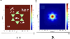
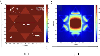
Figure 1 (a) shows the first computer model. A side of any of the nano triangles is 200 nm and the gap between the tips of two adjacent triangles is 25 nm. A constant thickness of the nanotriangles of 15 nm was assumed for all simulations.
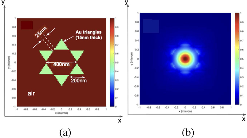
Figure 1: FDTD simulation of Au model: (a) First computer model of one unit cell of the Fischer pattern and (b) xy-plane distribution of the electric field intensity recorded 5 nm above the surface of the structure in (a).
The distribution of the electric field intensity in the xy-plane, parallel to the surface of the structure, is computed for x and y orientations of the dipole, respectively. The field distributions are recorded at a monitor set at a height of 5 nm from the structure surface. In order to model an unpolarised illumination condition, we averaged the electric field intensities obtained with the two orthogonal orientations of the dipole. The normalized and averaged electric field intensity distribution for an excitation wavelength of 532 nm is shown in Fig. 1 (b). The field distribution reveals a partial light penetration into the metal covered areas. As a result, the metallic elements cast partial shadows in the transmitted light.
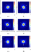
The dependance of the near-field on the orientation of the dipole is shown in Fig. 2. The electric field distribution in Fig. 1 (b) is an average over all six orientations of the dipole shown in Fig. 2. The average intensity is representative of the unpolarised incident illumination condition used in the experiments.
As seen in Fig. 2, the near-field intensity patterns depend on the orientation of the dipole. In particular the near-field pattern generated when the dipole orientation is parallel and perpendicular to the gap between the tips of adjacent triangular nanoelements. For example, orientations parallel to the gaps (30deg (Fig. 2 (a)), 30deg (Fig. 2 (c)), and 90deg (Fig. 2 (e))) appear to be different from orientations perpendicular to the gaps (60deg (Fig. 2 (b)), 120deg (Fig. 2 (d)), and 180deg (Fig. 2 (f))).
Averaging over any two pairs of orthogonal dipole orientations yields identical results. However, if we consider a structural anisotropy of the modeled structures, e.g. unequal gap distances between two adjacent elements, the effect of anisotropy in the simulation results can be ameliorated by averaging over all six polarization orientations. Averaging also makes the pattern more symmetric with regards to the central aperture. Nevertheless, penetration of light in metal covered areas, and light confinement in the central aperture region with similar intensities, is observed for all the considered dipole configurations irrespective of their alignment relative to the butterfly antennas.
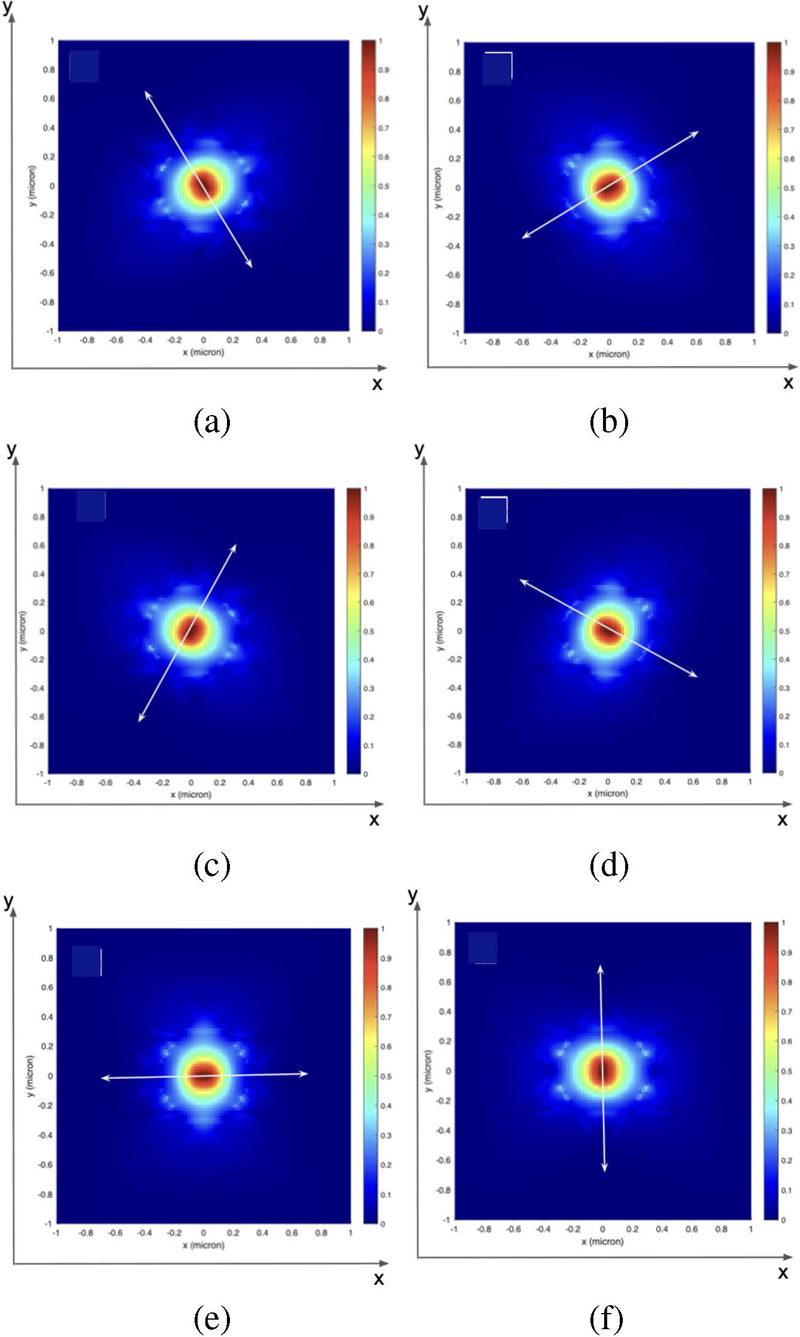
Figure 2: Field dependence on dipole orientation. Electric field intensity distribution in the xy-plane at a monitor height of 5 nm from the surface of the structure. Dipoles are oriented along directions parallel and perpendicular to each pair of gaps between adjacent nanotriangles. The dipole orientations are (a) 30deg, (b) 60deg, (c) 30deg, (d) 120deg, (e) 90deg, and (f) 180deg from the +y-axis, respectively.
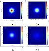
The dependence of the field distribution on the monitor distance is studied by increasing the monitor height in four steps from 10 nm to 200 nm from the surface of the structure. At each step (height along the z-axis), the corresponding electric field pattern is recorded for the three pairs of orthogonal in-plane orientations of the dipole excitation source, and averaged to mimic an unpolarised illumination condition. The aim of this study is to better predict the SNOM measurement conditions where the field distribution is recorded by an objective lens in the um-range away from the sample surface.
The normalized average intensity profiles for the four monitor heights of 10 nm, 50 nm, 100 nm, and 200 nm are shown in Fig. 3.
At a distance of less than 10 nm, light confinement is most pronounced and the shape of the center hexagonal aperture is more discernible. As the distance of the monitor is increased, the finer details of intensity variations gradually disappear from the near-field pattern. It indicates that the light confinement seen in the near-field is due to evanescent waves that dissipate with increasing the distance of the monitor from the surface of the nanostructure.
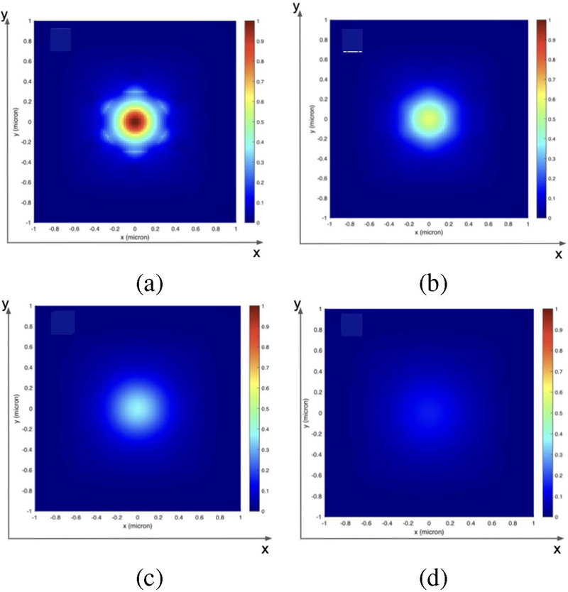
Figure 3: Field dependence on monitor height. Evolution of the field pattern with increasing height of the monitor from the surface of the structure. The averaged and normalized distribution of the electric field intensity in the xy-plane was calculated for a monitor z-distance of (a) 10 nm, (b) 50 nm, (c) 100 nm, and (d) 200 nm.
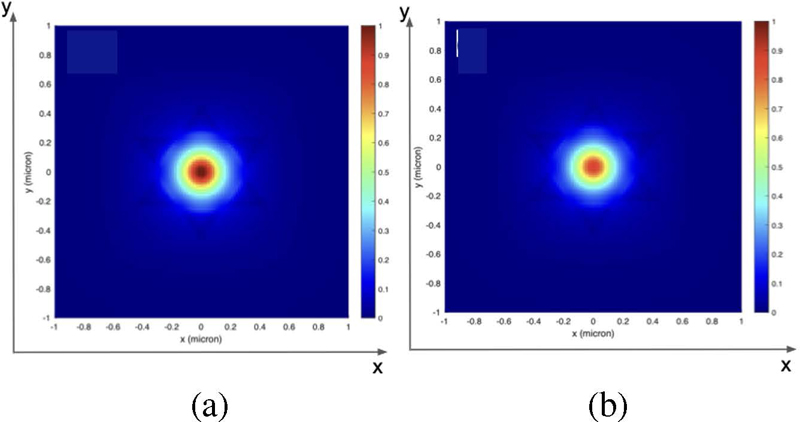
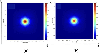
Figure 4: Field distribution with 405 nm excitation. The averaged and normalized field intensity distribution simulated for the geometry in Fig. 1 (a) for an excitation wavelength of 405 nm, at a monitor height of 5 nm. Field intensity pattern normalized to (a) the maximum intensity and (b) the maximum intensity found at 532 nm excitation from Fig. 1 (b).
A third main parameter influencing the near-field behavior of the nanoantenna is the pattern dimension compared to the excitation wavelength. The simulated field distribution of the first model (Fig. 1 (a)), obtained with an excitation wavelength of 405 nm, is shown in Fig. 4. In order to directly compare the result with the earlier shown intensity pattern after 532 nm laser excitation in Fig. 1 (b), the 405 nm intensity pattern (Fig. 4 (b)) is normalized using the maximum intensity found in Fig. 1 (b). Compared to Fig. 1 (b), Fig. 4 (b) shows that, at 405 nm excitation, the central higher intensity lobe diminishes both in size and intensity.
Figure 5 (a) shows the second computer model of an Al Fischer nanostructure with a larger central aperture of 1.1 um in diameter. A side of any of the triangular elements is 300 nm, the gap between the tips of two adjacent triangles is 250 nm, and the metal thickness of 15 nm is the same as used for the first model. Figure 5 (b) shows the normalized electric field intensity averaged over three pairs of orthogonal orientations of the dipole at an excitation wavelength of 532 nm and recorded at a monitor height of 5 nm.
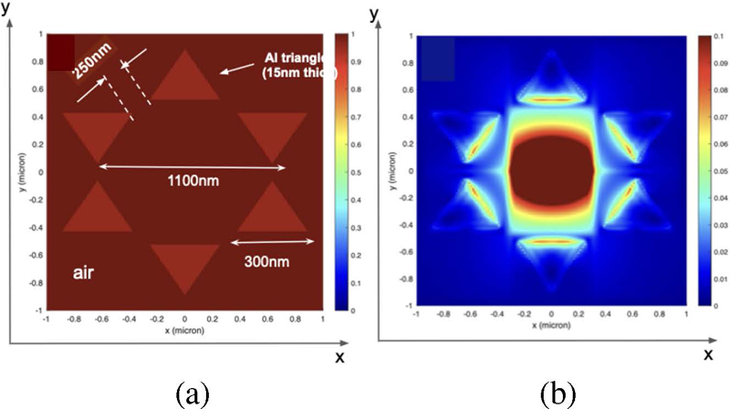
Figure 5: Second computed model of a 1.1 um Al pattern: (a) Computer generated model of a hexagonal arrangement of Al antenna elements with a central aperture diameter of 1.1 um and (b) xy-plane distribution of the electric field intensity at a monitor height of 5 nm for the structure in (a).
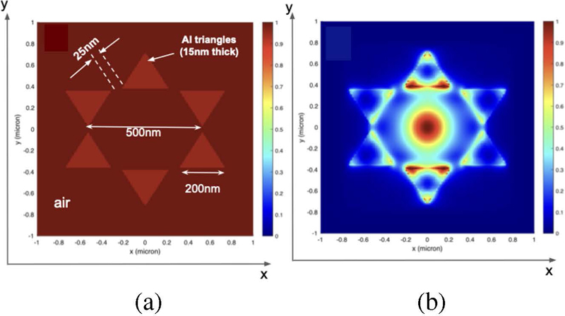
Figure 6: Second model of Al with reduced pattern diameter of 500 nm: (a) Geometry of nanoantenna elements with a central aperture diameter of 500 nm and (b) xy-plane distribution of the averaged and normalized electric field intensity at a monitor height of 5 nm from the structure surface.
Figure 5 (b) shows that light penetrates into metal covered antenna elements partially as in the case of the Au model (Fig. 1 (b)). However, the intensity and lateral depth of penetration is less. Most of the transmitted light intensity in Fig. 5 (b) originates from the central aperture, while only a small fraction is passed through the gaps in Fig. 5 (a).
Figure 6 (a) shows a slight variation of the second computer model where the central aperture diameter is changed to 500 nm. Figure 6 (b) depicts the corresponding distribution of intensity pattern. The intensity pattern shows strong enhancements along the edges and at the tips of the metallic antenna elements.
III. SNOM SETUP
A commercially available Raman/SNOM system based on a confocal microscope (WITec alpha300) [8] was used to study microscopy resolution and electric field enhancement effects. In the Raman and Photoluminescence mode the maximum spatial resolution is diffraction limited by the chosen objective lens and restricted to 300-400 nm (532 nm excitation wavelength, 100x objective lens with NA0.9) [4, 10]. However, confining the excitation spot by introducing an aperture can help to overcome the diffraction limit. This principle is used in the SNOM mode, where a hollow truncated pyramid is scanned in contact mode across the sample surface. The height control is achieved by an atomic force microscopy-like feedback loop, allowing to simultaneously record the sample topography (height information) and SNOM intensity [9–10].
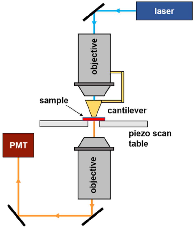
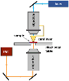
Figure 7: Schematics of the transmission SNOM setup used in our experiments.
SNOM was performed in the transmission geometry (Fig. 7). An excitation laser is focused by a 20x objective lens (NA0.4) on the backside of an aluminum coated silicon cantilever which acts as a near-field SNOM excitation probe [9–10]. The apex opening of the cantilever directly defines the spatial resolution. For our study, two different tip sizes of 90 nm and 150 nm were used to investigate the maximum achievable spatial resolution and the influence on the signal-to-noise ratio (SNR).
The transmitted light from the sample is collected by a long-range 100x (NA0.75) objective lens and detected using a photomultiplier tube (PMT). By lateral scanning of the sample under the SNOM tip, spatially resolved maps of the transmitted SNOM intensity and topography across the sample could be generated. To analyze the multidimensional dataset as well as to control the microscope system, WITec software Control 6 and Project 5 were used.
IV. MEASUREMENT RESULTS
Achieving a high image quality and lateral resolution in a SNOM system most importantly relies on the cantilever tip size and quality as well as the chosen excitation conditions. The influence of those parameters were investigated on commercially available metallic projection patterns provided by Kentax GmbH [11]. To fabricate these samples, monolayers of hexagonal closely packed latex spheres are used as a mask for physical vapor deposition of a 10 nm Al or Au layer. After removal of the latex spheres, the resulting structure consists of a periodic hexagonal metal array deposited on a 0.15 mm-thick glass substrate.
Lower resolution scans covering an area of 5 um 5 um (scan resolution 50 nm) on Au Fischer pattern featuring a central aperture diameter of about 400 nm are depicted in Fig. 8. The top row shows the sample topography (height map) while the SNOM intensity profile is visualized in the bottom row. The images are complementary. Metal coated areas are opaque for the excitation laser and light is backscattered towards the incident direction. Those regions appear as black dots, while bright areas originate mainly from areas not covered by metal.
The SNOM resolution is basically defined by the geometric confinement (tip aperture). Any scattering and diffraction loss at the cantilever tip is expected to have a negligible effect. This is because the tip is scanned in contact mode across the sample surface, exciting the near-field. Changing the excitation laser wavelength and keeping the tip opening aperture constant should have a negligible influence on the resolution since both laser wavelength are almost similar (d), and pass the same tip aperture. These expectations are confirmed by the scans shown in Fig. 8. Altering the excitation wavelength from 405 nm (Fig. 8 (a)) to 532 nm (Fig. 8 (b)) doesn’t change the SNOM intensity pattern significantly. On the other hand, the chosen cantilever opening is seen to mainly determine the lateral SNOM resolution. Smaller and more crisp features are obtained using the smaller 90 nm tip (Fig. 8 (b)) compared to the more than twice as large 150 nm tip (Fig. 8 (c)).
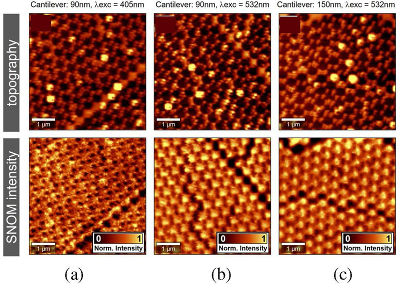
Figure 8: Cantilever tip size and excitation wavelength dependency. Topography (top row) and SNOM intensity (bottom row) for a hexagonal Au pattern having a central aperture diameter of d400 nm. Different excitation and scan conditions were investigated: (a) 90 nm cantilever opening in conjunction with an excitation wavelength of 405 nm, (b) 532 nm, and (c) a 150 nm tip together with 532 nm.
Besides the resolution, the achievable SNR is an important SNOM parameter. A higher SNR enables faster, more stable, scans (less sample drift), and stronger SNOM intensity signals. Due to a higher output power of the 532 nm laser, the SNR after 532 nm excitation (Fig. 8 (b)) is increased compared to 405 nm (Fig. 8 (a)). For the 405 nm laser (Fig. 8 (a)), an almost constant background intensity over the whole scan area is detected, at 532 nm excitation the dominant SNOM signal originates from the center part of the hexagonal shaped Fischer pattern. A closer look at the edges and gap regions between the butterfly pattern reveal fine details which could not be resolved at 405 nm excitation. This observation reveals the importance and influence of the SNR on theresolution.
Figure 9 shows the images of a 2 um 2 um scan with two different tip sizes. A clear superior topography height contrast (top row of Fig. 9), and a significantly improved SNOM resolution was achieved using the 90 nm cantilever. Edges appear fuzzy in the SNOM intensity image using the 150 nm tip (Fig. 9 (b)). In comparison, fine lines connecting adjacent hexagonal transmissive parts as well as light from metal covered areas are resolved using the 90 nm cantilever (Fig. 9 (a)). It should be highlighted that there is a small lateral shift expected between the topography and SNOM intensity images. Due to the finite cantilever thickness at the apex (rim), the topography signal will respond first to any height change at the metal pattern edge, followed by the intensity signal when light is transmitted through the cantilever tip opening [9].
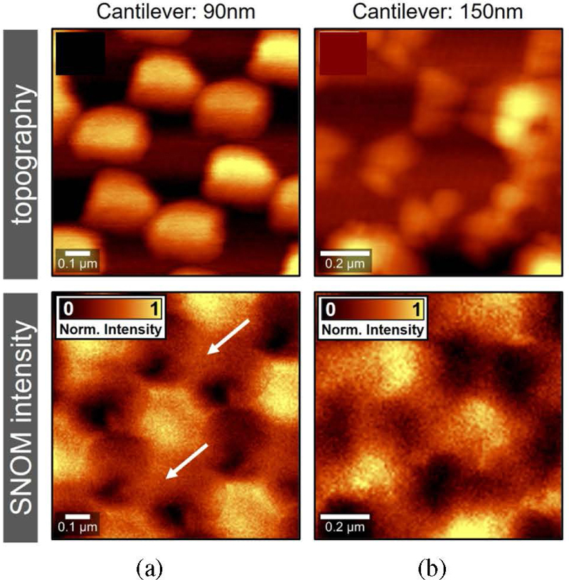
Figure 9: High resolution SNOM measurements. Topography (top) and SNOM intensity (bottom) for the same Au sample investigated in Fig. 8 using (a) 90 nm and (b) 150 nm tip opening.
Summarizing our instrument related SNOM study, the optimum measurement conditions to achieve high resolution and a high SNR for our system are found for a cantilever with the smallest available opening of 90 nm and using a high power laser emitting at 532 nm.
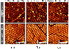
The influence of pattern size on light-matter interaction is highlighted in size series in Fig. 10. Aluminum Fischer pattern with an intended central aperture diameter ranging from 230 nm (d) up to 1.1 um (d) were investigated. First it should be noted that the smallest pattern with an intended central aperture diameter of 230 nm shows the potential of SNOM in terms of resolution. Features below the theoretical diffraction limit for optical microscopy are observed. The topography images in the top row of Fig. 10 as well as SNOM intensity (bottom row) reveal features on a lateral length scale below 100 nm. However, due to fabrication inhomogeneities and absent hexagonal features, the 230 nm pattern cannot be used to study the change of the near-field intensity as the Fischer pattern size increases.
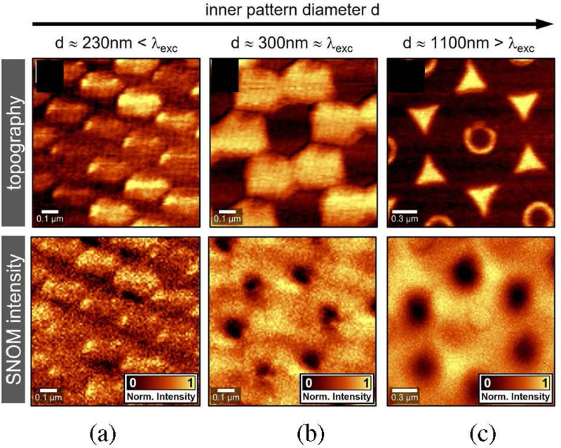
Figure 10: Aluminium Fischer pattern size series. Fischer patterns with a central aperture diameter ranging from (a) intended 230 nm to (c) 1.1 um were investigated using the best known SNOM conditions: 90 nm tip and 532 nm laser excitation.
By enhancing the pattern size from 300 nm to 1.1 um, a change in the morphology is observed. The 1.1 um structure (Fig. 10 (c)) exhibits a well separated triangular pattern with noticeable gaps in between. For 300 nm (Fig. 10 (b)), the gaps are nearly closed and a hexagonal symmetry of the metal parts is present. Classically one would expect almost no light transmitting through the small or almost closed gaps between the pattern. However, in the SNOM intensity image (Fig. 10 (b), bottom), transmitted light is also detected in areas covered by metal. We attribute this to a field enhancement effect which is expected to be more pronounced when the feature size is close to the laser wavelength. This hypothesis is confirmed by the measurement at the d400 nm gold pattern shown in Fig. 9 (a). The light enhancement and propagation in the metal covered area is even more pronounced. Note the extended bright lines/features exceeding the expected gap opening between adjacent hexagonal metal patterns and connecting different bright hexagonal openings (examples highlighted by arrow in Fig. 9 (a)).
A further increase of the pattern size to d (Fig. 10 (c)) marks the transition to the classical regime in which the transmitted light originates mainly from the center aperture of the Fischer pattern and the larger gap openings between adjacent metal structures.
V. DISCUSSION
As highlighted in Section II, partial light penetration and confinement is observed for the metallic nanoantenna array at a monitor distance less than 10 nm from the surface of the nanostructures (Fig. 1 (b), 3 (a)). Light is predominantly transmitted through the transparent, central aperture of the Fischer pattern for all investigated diameter sizes, ranging from 300 nm to 1.1 um (Figs. 1 (b), 5 (b), and 6 (b)). In addition, antenna elements cast a partial shadow blocking the light from passing through these areas. Those findings are validated by SNOM measurement results depicted inFigs. 9 and 10.
In order to allow for a comparison between our simulations and the measurements, the modeled conditions were adjusted to the experimental ones. A main difference between the simulated and measured intensity maps is the occurrence of more details or finer intensity gradations in the simulated patterns. This is most pronounced for the light transmitted through the central aperture. While the measurement results, e.g. Fig. 9 (a), show only a weak intensity reduction from the center of the inner aperture to the outer regions close to the metal pattern, the computed center field distribution in Fig. 1 (b) consists of concentric rings with gradually reduced intensity. Starting at a maximum intensity of 100% in the middle of the center aperture, the value drops to 40% close to the edges of the metal covered regions adjacent to the center aperture.
This observation could be explained considering the change of the near-field intensity distribution with increasing monitor height, summarized in Fig. 3. As the monitor height increases to 50 nm and 100 nm, the finer intensity variations in the center aperture area slowly disappear and the absolute intensity value reduces significantly. For the measurement configuration used, the objective lens to collect the transmitted light is actually at a larger distance compared to the maximum simulated monitor distance of 200 nm (Fig. 3 (d)). Therefore only a small intensity variation in the center aperture part as well as a reduced overall intensity isexpected.
Furthermore the chosen excitation wavelength and power will affect the intensity gradation observed in the center aperture part. Lowering the excitation wavelength from 532 nm (Fig. 1 (b)) to 405 nm (Fig. 4 (b)) results in a smaller lateral extension of the center intensity distribution, which reduces the ability to resolve finer intensity features. Evidence for an experimental confirmation of this simulation result are given in Figs. 8 (a) and (b). Only a very small intensity enhancement in the center of the clear aperture region of the Fischer pattern is found for 405 nm excitation. The transmitted SNOM intensity is almost homogeneously distributed across the whole scanned area, in contrast to the 532 nm laser scan (Fig. 8 (b)). The center part of the aperture is clearly of highest intensity and the intensity is reduced towards the edges of the center aperture. This observation is in good agreement with the simulation shown in Fig. 1 (b) for the pattern center region.
However, in experimental investigations the laser power and therefore the achieved signal-to-noise ratio needs to be considered. Since the output power for the 532 nm laser is larger compared to that of the 405 nm laser, the transmitted SNOM intensity and SNR is enhanced in the first case. This will help to resolve finer intensity details in the SNOM image as seen in Figs. 8 (a) and (b). Consequently, our best measurement conditions are found at high power 532 nm excitation using a small cantilever tip size, which was 90 nm inour case.
Finally we discuss the role of the pattern size on the simulated and measured field distribution. Of particular interest are light-matter interaction effects like field enhancement, and surface plasmonic resonances.
With Al nanostructure, two different pattern sizes with 1.1 um and 500 nm center aperture diameter, excited at 532 nm were considered. When the diameter is larger than the excitation wavelength (d1.1 um, Fig. 5), light is mainly transmitted through the center part and less from the gap regions between adjacent triangles of the butterfly antennas. However, light originating from areas covered by metal is predicted. Those regions are localized at the lower edges of the triangles closest to the center aperture.
Reducing the diameter size to a regime comparable to the excitation wavelength (d500 nm) increases the probability of observing phenomena like light penetration in metal covered areas and plasmonic effects. For the 500 nm Al Fischer pattern in Fig. 6, light coming from the lower triangular sides is strongly intensified, while the transmission through the center aperture is more localized featuring a clear intensity gradient towards the edges of the center aperture. In addition, localized spots of highest intensity, which is comparable to the one observed in the aperture center, are forming at the tips of the triangles. This behavior could be related to a localized surface plasmon resonance(LSPR).
The Fisher pattern size dependent SNOM measurements in Fig. 10 show indications which support the simulation results. In the case d (Fig. 10 (c)), dominant emission is observed from the aperture center and the gap regions of the triangles. In contrast, for a smaller center aperture diameter (d in Fig. 10 (b)), the transmitted light seems to be more centered to the aperture origin and weaker in the gap regions between adjacent triangles. This observation is supported and even more pronounced for the d400 nm gold pattern depicted in Fig. 9 (a). Light from the gap regions is suppressed and mainly transmitted in the center part of the aperture. Furthermore, indications of a higher intensity at the lower triangle edges close to the central aperture can be assumed, which is predicted by the simulation in Fig. 1 (a). However, an experimental verification of fine details of the field intensity distribution as projected by the simulation is challenging. Besides the cantilever tip size, its quality, and the excitation wavelength, mainly the distance of the collecting objective lens from the sample reduces the lateral resolution substantially. This phenomena was discussed earlier and is in agreement with the simulation data in Fig. 3.
VI. CONCLUSION
In summary, we investigated the near-field intensity distribution generated through light interaction with butterfly nanoantennas, both using FDTD simulations with computer generated models, and SNOM measurements at commercially available Fischer patterns. Essential agreement between the simulation and the key experimental observations are found.
Of special interest was the light enhancement by the nanoantennas. Light confinement, field enhancement, and light intensity from metal covered areas are observed in the d regime. For large patterns (d), the intensity distribution is seen to be dominated by fundamental transmission and reflection from the metalpattern.
The best experimental conditions to achieve highest lateral resolution and investigate light-matter interaction signatures can be achieved by using the smallest SNOM cantilever size available, high power excitation (high signal-to-noise ratio), and beneficially a small detector distance relative to the sample. A maximum lateral resolution smaller than 100 nm and well below the diffraction limit for optical microscopy was achieved using a 90 nm SNOM cantilever opening and 532 nm excitation.
ACKNOWLEDGMENT
The authors would like to thank our Meta colleagues Kathryn M. Kelchner, John Roberts, Guillaume Lheureux, Yaniv Vinish, Shuyu Bao, and Matthias Finger from WITec (Oxford Instruments) for the useful discussions. N.M.P. would like to gratefully acknowledge Prof. Junichiro Kono and Prof. Geoff Wehmeyer from Rice University for their support during hisinternship.
REFERENCES
[1] T. H. Taminiau, F. B. Segerink, R. J. Moerland, L. (Kobus) Kuipers, and N. F. van Hulst, “Near-field driving of a optical monopole antenna,” Journal of Optics A: Pure and Applied Optics, vol. 9, no. 9, p. S315, Apr. 2007.
[2] U. C. Fischer, J. Heimel, H.-J. Maas, H. Fuchs, J. C. Weeber, and A. Dereux, “Super-resolution scanning near-field optical microscopy,” in Optical Nanotechnologies, J. Tominaga and D. P. Tsai, Eds. Berlin Heidelberg: Springer-Verlag, 2003, pp. 141-153.
[3] L. E. Hennemann, A. Kolloch, A. Kern, J. Mihaljevic, J. Boneberg, P. Leiderer, A. J. Meixner, and D. Zhang, “Assessing the plasmonics of gold nano-triangles with higher order laser modes,” Beilstein Journal of Nanotechnology, vol. 3, pp. 674-683, 2012.
[4] J. Toporski, T. Dieing, and O. Hollricher, Confocal Raman Microscopy, 2nd ed. New York: Springer, 2018.
[5] K. S. Yee, “Numerical solution of initial boundary value problems involving Maxwell’s equations in isotropic media,” IEEE Trans. Antennas Propagat., vol. AP-14, pp. 302-307, 1966.
[6] A. Z. Elsherbeni, FDTD Course Notes, Department of Electrical Engineering, The University of Mississippi, MS, Spring 2001.
[7] Ansys Lumerical FDTD [Online]. Available: https://www.ansys.com/en-gb/products/photonics/fdtd.
[8] Oxford Instruments, “alpha300 S - SNOM microscope” [Online]. Available: https://raman.oxinst.com/products/scanning-probe-microscopes/snom-alpha300s.
[9] WITec Project FIVE, software 5.5, suite help function.
[10] Oxford Instruments, “Scanning near-field optical microscopy (SNOM)” [Online]. Available: https://raman.oxinst.com/techniques/snom.
[11] Kentax.de UHV equipment, “Projection pattern” [Online]. Available: https://www.kentax.de/projection-pattern.html.
BIOGRAPHIES

Saswatee Banerjee is currently working as Research Scientist at Meta Ireland, Cork, Republic of Ireland. Her research interests include optical design, simulation methods and light propagation in nano-optic and photonic components. Before joining Meta, she worked in Japan for 20 years in both industrial R&D and academia.

Nicolas Marquez Peraca is a 5th year Ph.D. Candidate in the Department of Physics and Astronomy at Rice University in Houston, TX, USA. Before coming to Rice in 2018, he was a Guest Researcher for 2 years at the National Institute of Standards and Technology, where he worked on the electric and opto-electronic characterization of multi-junction solar cells. He joined Meta’s Display & Optics team in Cork, Republic of Ireland, in the fall of 2022 as a Research Scientist Intern. His current research interests include ultrafast phenomena in condensed matter physics, THz magneto-spectroscopy of quantum materials, and AR/VR metrology.

Alexander Franke is currently working in the Display & Optics team of Meta in Cork, Republic of Ireland. Prior to joining Meta he worked in academia and R&D at various locations in Germany and USA, including the University of Magdeburg, TU Berlin, North Carolina State University, and the Fraunhofer Institute for Solar Energy Systems in Freiburg, Germany. His research interests are wide spread ranging from crystal growth (epitaxy), optoelectronic devices, photonics, nanostructures, to metrology and especially optical characterization by various spectroscopic methods.
ACES JOURNAL, Vol. 39, No. 2, 130–138
doi: 10.13052/2024.ACES.J.390206
© 2024 River Publishers