A Symmetrical Fractal-based Balanced Branch-Line Coupler for Simultaneous Low- and Mid-band 5G Frequencies Applications
Abdulkadir B. Shallah, Farid Zubir, Mohamad Kamal A. Rahim, and Zubaida Yusoff
1Wireless Communication Centre, Universiti Teknologi Malaysia, 81310 Johor Bahru, Johor, Malaysia
shallah@graduate.utm.my, faridzubir@utm.my
2Communication Engineering Department, Faculty of Electrical Engineering, Universiti Teknologi Malaysia, 81310 Johor Bahru, Johor, Malaysia
mdkamal@utm.my
3Faculty of Engineering, Multimedia University, Persiaran Multimedia, 63100 Cyberjaya, Selangor, Malaysia
zubaida@mmu.edu.my
Submitted On: September 27, 2023; Accepted On: January 9, 2024
ABSTRACT
Symmetry is a key factor for Branch-Line Couplers (BLCs) in RF and microwave systems. This balanced approach evenly distributes power between two output ports, aiding impedance matching and reducing unwanted coupling and crosstalk, while increasing input-output isolation. Furthermore, the symmetrical design of BLCs ensures favorable return loss and phase balance, which are essential for phase-sensitive detectors and beamforming. This symmetry also guarantees consistent performance over a wide frequency range, making it suitable for broadband or multi-frequency applications. We present a compact BLC operating in two frequency bands, ideal for 5G sub-6 GHz applications. It uses T-shaped lines with folded lines and stubs in a Minkowski fractal shape, resulting in a size reduction of 90. The design and simulation were performed using the CST Microwave Studio at 0.7 GHz and 3.5 GHz, achieving a new high frequency band ratio of 5. A prototype on Rogers RT5880 substrate ( mm) was tested to validate the design’s effectiveness, offering potential for modern wireless applications requiring versatile frequency band operation.
Index Terms: Balanced, Coupler, Fifth-generation, Fractal, Frequency ratio, Low-band, Mid-band, Minkowski, Simultaneous, Symmetrical.
I. INTRODUCTION
Recent advancements in technology and communication systems have spurred a growing demand for compact, multifrequency, and high-bandwidth devices to enhance circuit designs’ efficiency and performance [1]. In the realm of microwave and millimeter wave frequencies, maintaining symmetry in the design of microstrip couplers plays a crucial role in ensuring equal power distribution while minimizing undesirable coupling effects [2]. However, traditional BLC with four ports, including an input port, an isolated port, and two coupled ports with a 90 phase difference, no longer meet the requirements of modern device design trends, which emphasize the need for dual-band or multiple-band functionality [3].
Various methods have been proposed to achieve dual frequency operation in BLCs, including the introduction of stubs in [4, 5] or -shapes [6, 7] and coupling lines [8, 9] to convert single-band sections into dual-band counterparts. However, these approaches exhibit limitations such as large circuit sizes, small frequency ratios, complex structures, high insertion loss, and a restricted frequency range, making them unsuitable for lower 5G bands, such as 0.7 GHz and 3.5 GHz [10]. Recent research has reported dual-band BLCs with higher frequency ratios [11, 12], but their optimal performance is observed when the midpoint frequency is higher than 3 GHz.
To address the demands of lower sub-6 GHz 5G frequency bands with a wide frequency ratio, this paper introduces a compact and simple dual-band BLC design. It uses T-shaped technique with folded lines in the form of Minkowski fractal geometry (MFG) to achieve compact packing of transmission lines (TL), effectively reducing the overall size in comparison to traditional configurations. The paper presents analytical equations, design details, and prototype realization of this dual-band branch-line coupler (DB-BLC), showing excellent agreement between measured and simulated results at frequencies below 4 GHz. In addition to 5G applications, the proposed BLC can be used in radar systems, where it can split incoming and outgoing signals between radar transmitters and receivers, facilitating tasks such as topography measurement, vegetation analysis, and weather monitoring [13].
II. DESIGN ANALYSIS OF THE DUAL-BAND STRUCTURE
A. Dual-band branch-line coupler
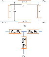
The traditional BLC’s -wave sections are transformed into dual-band equivalents by adding extra T or stubs. In this work, we adopt the T-shaped TL approach for simplicity. Figures 1 (a) and (b) show the layout of a standard BLC and how the -wave sections are converted into T-shaped segments. This design equates the ABCD matrix of the conventional -wave TL to the ABCD matrix of the T-shaped segments as:
| (1) |
and represent the ABCD matrices for the T-section’s series and shunt elements, respectively.
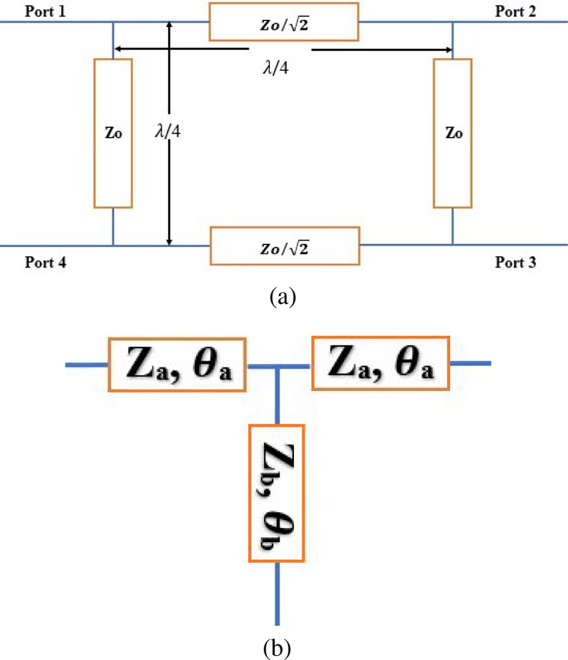
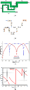
Figure 1: The layout diagram of (a) conventional BLC and (b) proposed T-section.
And the ABCD matrix of the wave transmission line is given by:
| (2) |
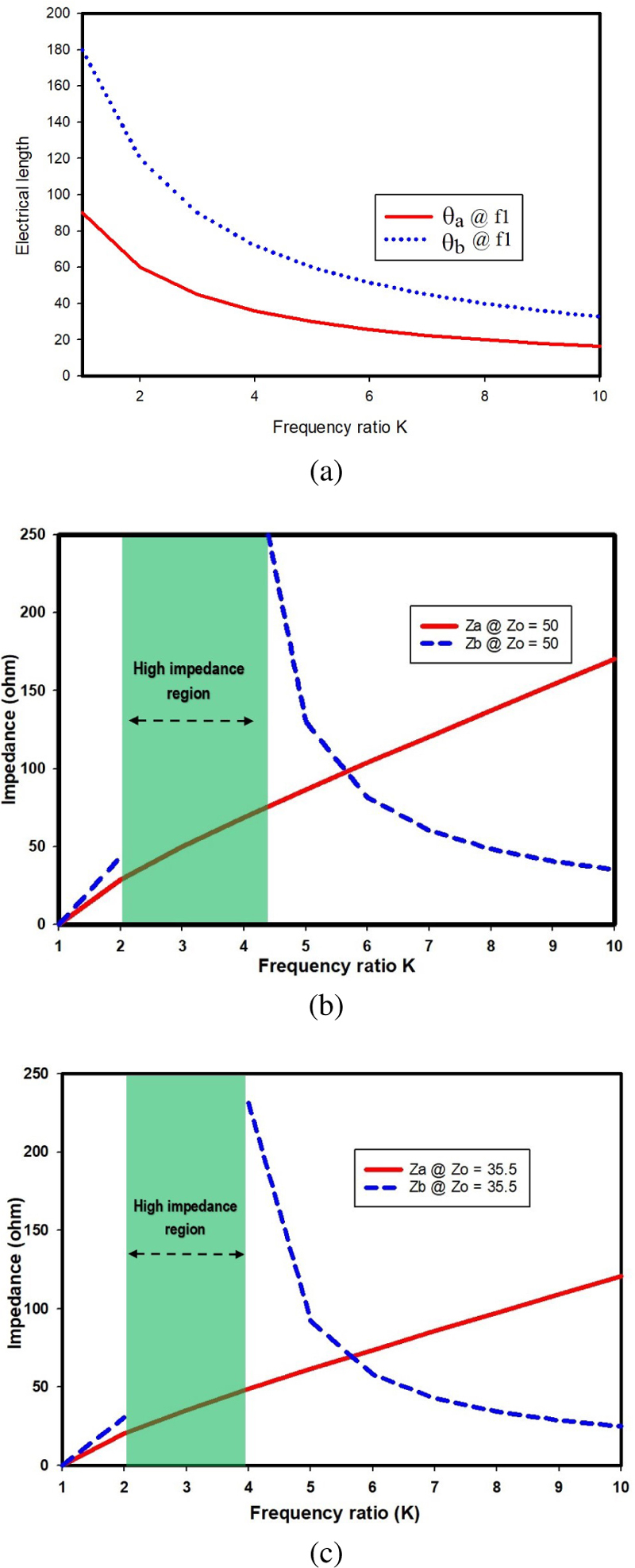
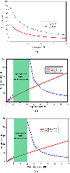
Figure 2: The relationship between (a) the electrical lengths and the frequency ratio K, (b) the relationship between the () when and frequency ratio K, and (c) the relationship between when and the frequency ratio K.
Having as the characteristic impedance of the primary branch line. The solutions to equations (1) and (2) results in:
| (3) |
| (4) |
where and represent the electrical lengths of the lines at designed frequencies. Furthermore, the solution to equation (4) is obtained as:
| (5) |
| (6) |
Therefore, from equations (3) and (5), we have:
| (7a) | |
| (7b) |
The values for the line impedances can be deduced using the following equations:
| (8a) | |
| (8b) |
Table 1: The dimensions based on the theoretical parameters
| Parameter | Z () | Width (mm) | Length (mm) |
|---|---|---|---|
| L | 61.25 | 1.77 | 52.08 |
| L | 86.60 | 0.95 | 54.37 |
| Ls | 91.88 | 0.90 | 51.70 |
| Ls | 129.90 | 0.45 | 54.30 |
By using equations (1) to (8), we can understand how electrical lengths change with the frequency ratio K, as shown in Fig. 2 (a). We also explore the behavior of characteristic impedances, denoted and , in our design. These operate at two different impedance values: and . Figures 2 (b) and (c) illustrate how these impedance values change with the frequency ratio K.
The practical impedance range for is 22.5 to 180 , as shown in Figs. 2 (b) and (c). This limits frequency ratios K to 1.93-2.33 and 3.5-8.7. Achieving ratios between 2.34 and 3.49 is challenging due to high impedance.
Alternatively, in [11, 12], coupled lines achieve 2.34-3.49 ratios, but suffer high insertion loss [14]. T-sections in BLC [15, 16, 17] have limited ratios. For example, [15] and [16] achieve 2.22 and 2.42 ratios at 0.9/2 GHz and 2.4/5.2 GHz. The highest ratio in [17] is 4.8.
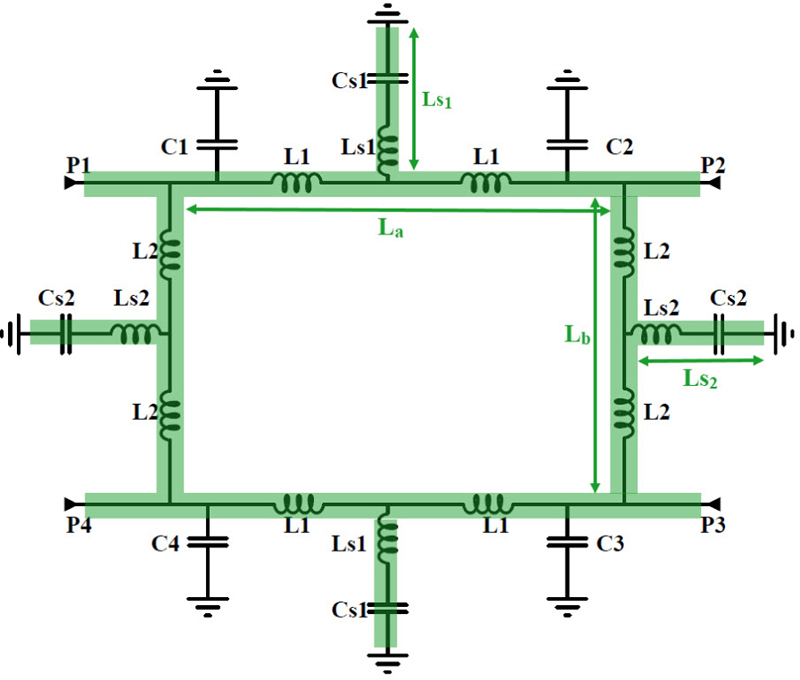
Figure 3: The lumped elements representation superimposed with the layout of the DB-BLC 1.
Our work achieves a ratio of 8.7, offering greater versatility for dual-band BLCs, as shown in Figs. 2 (a-c), Fig. 3 displays lumped elements in DB-BLC 1, designed using Table 1 parameters.
While DB-BLC 1 covers a wide frequency range, it is bulky at (162.58 mm 161.31 mm). To reduce size, we fractalize the structure with sharp-edged chamfered bends to minimize capacitive effects [18].
B. Proposed miniaturized (DB-BLC 2)
To simplify the structure, we have modified the BLC series, shunt segments, and their stubs to resemble the first iteration MFG design. This change maintains device symmetry for reliable power distribution, strong isolation, consistent frequency response, low return loss, and phase balance, all vital for proper functionality.
The MFG implementation is based on three key parameters, as shown in Fig. 4: for generator length, for the indentation width, and for the depth of the fractal or indentation. Figure 4 (a) illustrates the evolution from the generator to the first Minkowski fractal iteration. We use the one-third ratio, common in creating famous fractal curves such as the Koch and Cantor geometries [19], which is crucial.
The dimension D values follow logarithmic functions defined in equation (9). k denotes the number of segments in the geometry, and r signifies the segments divided during each iteration after initially dividing the geometry into k segments.
| (9) |
Equation (9) yields a Minkowski fractal dimension of 1.465, which quantifies a fractal curve’s space-filling ability. In particular, not all fractal curves are suitable for use in BLC design, although some have found success in antenna design [20]. This distinction arises from the different input-output coupling requirements in the BLC design.
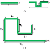
To enhance the coupling and establish a practical fractal dimension range, we adopt a first-iteration geometry. We replace the standard 1/3 ratio for generating diverse fractal curves with an arbitrary ratio. Figure 4 (a) shows the initial iteration with five segments, two horizontal sections () considerably longer, and three segments approximately and in length.
The characteristic impedances for main-series and shunt TLs remain unchanged to maintain desired dimensions. However, equations (7a) and (7b) undergo adjustments. Electrical lengths for main lines (-) and stubs (-) in Fig. 4 (b) are calculated based on the chosen arbitrary ratio, and the total length is given in equation (10).
The optimized dimensions for the proposed horizontal and vertical line sections are summarized in Table 2:
| (10) |
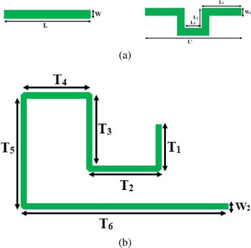
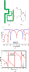
Figure 4: The layout representations of (a) initiator and fractalized main line and (b) stub.
Table 2: The optimized geometrical dimensions
| Section | Series Line | Shunt Line | Elect., Length | Series Stub | Shunt Stub |
|---|---|---|---|---|---|
| (mm) | 15.51 | 16.64 | 19.20 | 17.50 | |
| (mm) | 3.87 | 4.20 | 5.20 | 6.40 | |
| (mm) | 7.80 | 8.32 | 9.60 | 6.70 | |
| (mm) | 3.66 | 4.50 | 4.10 | 4.95 | |
| (mm) | 7.25 | 6.00 | 8.11 | 6.60 | |
| (mm) | 6.75 | 7.00 | 7.50 | 7.70 | |
| (mm) | 7.25 | 9.00 | 8.11 | 9.90 | |
| (mm) | 9.55 | 9.00 | 10.7 | 9.90 | |
| (mm) | 17.25 | 18.00 | 19.3 | 19.8 | |
| (mm) | 1.77 | 0.95 | |||
| (mm) | 0.85 | 0.55 |
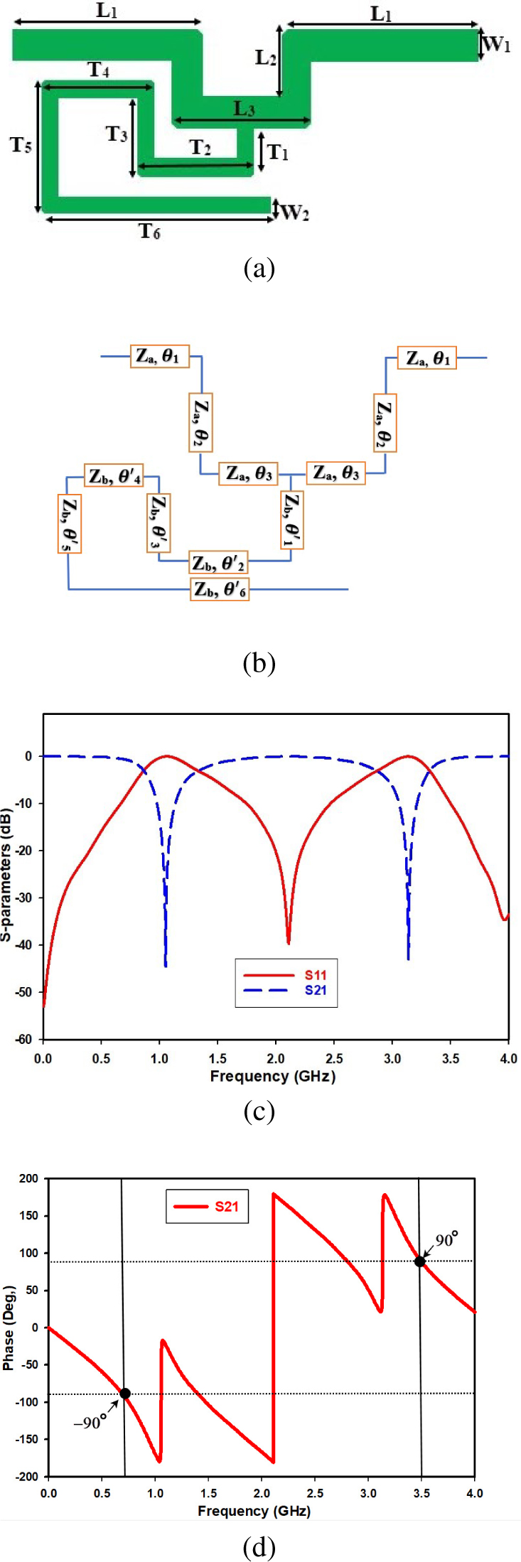
Figure 5: The representations of (a) 35.35 horizontal section, (b) equivalent circuit, (c) S-parameter response, and (d) phase response of the line.
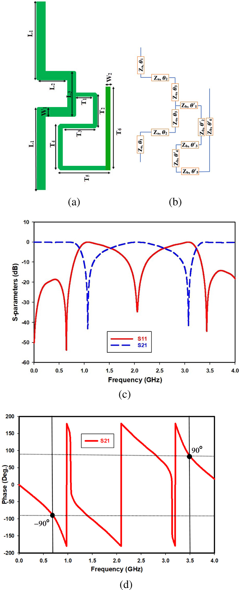
Figure 6: Representations of (a) 50 vertical section, (b) equivalent circuit, (c) S-parameter response, and (d) phase response of the line.
Figures 5 (a) and (b) display a compact 35.35 horizontal TL for efficient signal transmission at 0.7 GHz and 3.5 GHz. Our aim is minimal signal loss (low ) and minimal reflection (-10 dB) to optimize power transfer.
Figures 5 (c) and (d) show the TL’s magnitude and phase responses at 0.7 GHz and 3.5 GHz, providing a comprehensive view of signal behavior. In particular, Fig. 5 (d) achieves phase control with -90 and +90 at 0.7 GHz, and 3.5 GHz.
Figures 6 (a) and (b) detail the 50 vertical TL design and structure, revealing its physical arrangement. On the contrary, Figs. 6 (c) and (d) analyze the vertical TL’s S parameters and phase response, offering insights into system performance.
These figures highlight the vertical TL’s impressive capabilities, ensuring effective signal transmission at 0.7 GHz and 3.5 GHz and precise phase shifts of 90 and 90 at these frequencies. These results affirm the vertical TL’s reliability and significance in the system.
III. SIMULATIONS, FABRICATION, AND MEASUREMENTS
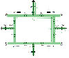
DB-BLC 1 and DB-BLC 2 were created for 5G below 6 GHz frequencies (specifically, 0.7 GHz and 3.5 GHz) using CST Microwave Studio software. DB-BLC 2, shown in Fig. 7, has a unique symmetrical design achieved by combining the TLs from Figs. 5 and 6. The gaps shown from the diagram are only for the purpose of demonstrating integration and do not reflect the actual configuration. It was developed on an RT/Duroid 5880 substrate, 0.787 mm thick, with a permittivity of 2.2 and a loss tangent of 0.0009.
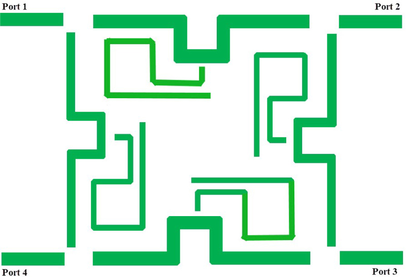
Figure 7: The diagram showing the assembly process of the Minkowski-shaped DB-BLC 2.
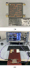
To realize the prototype shown in Fig. 8 (a), the photoetching technique was used and SMA connectors were used for measurements. The S parameters of the prototype were measured using a Rohde Schwarz ZNB 40 vector network analyzer (VNA), as illustrated in Fig. 8 (b).
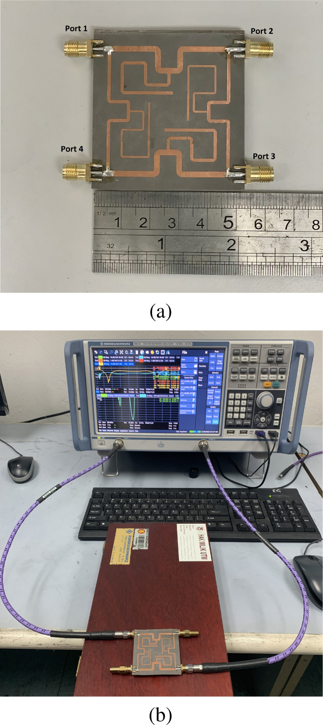
Figure 8: The structure of the fabricated prototype for BLC-2 (a) with SMA connectors and (b) with VNA during S-parameter measurement.
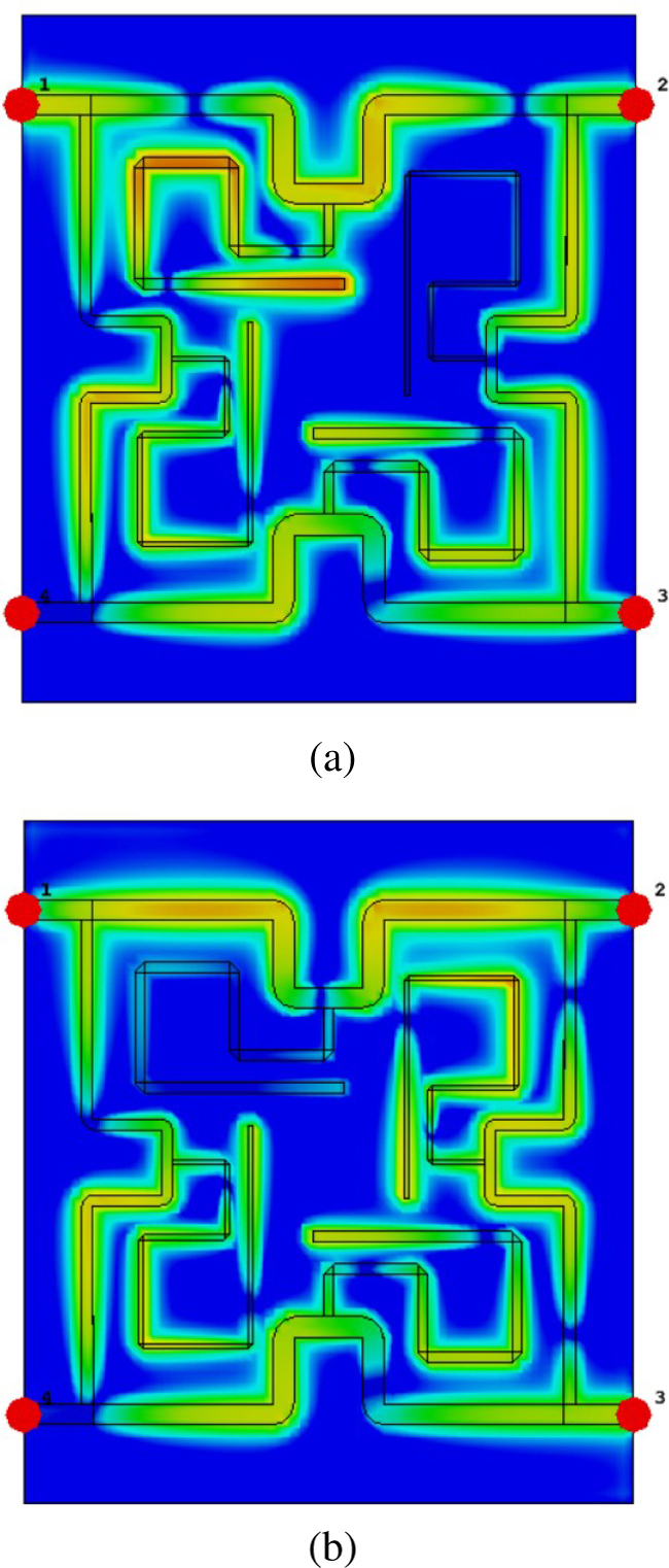
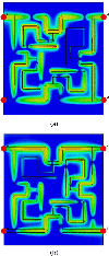
Figure 9: The current density distribution of the proposed DB-BLC 2 with Port-1 as an input port (a) at 0.7 GHz and (b) at 3.5 GHz.
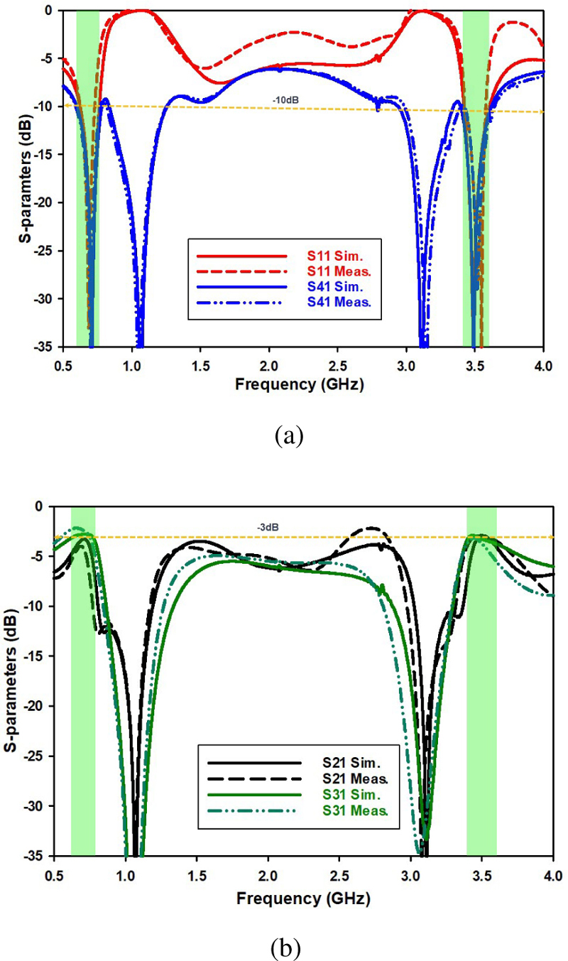
Figure 10: The S-parameters results analysis of DB-BLC 2 (a) and simulated and measured and (b) and simulated and measured.
IV. RESULTS AND DISCUSSION
Figures 9 (a) and (b) visually depict the current density distribution in the DB-BLC 2 structure at two critical frequencies, 0.7 GHz and 3.5 GHz. Figure 9 illustrates the equal division of the input signal between Port-2 and Port-3, with Port-1 as an input port, ensuring symmetric power distribution. This balance enhances device efficiency. Additionally, Port-4 remains isolated from the input signal, as evident in the figures, preventing unwanted signal leakage or interference at specified frequencies.
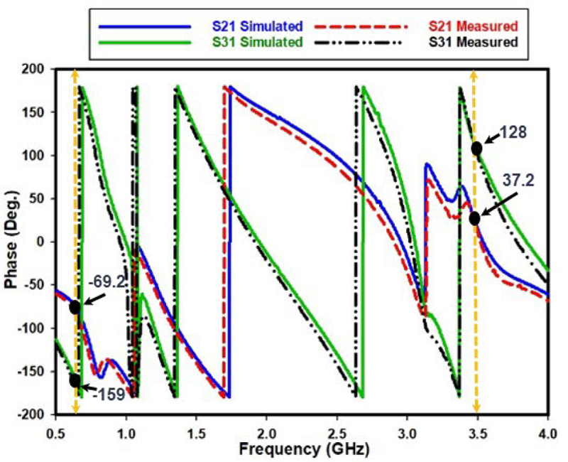
Figure 11: The overlapped phase response of the proposed DB-BLC 2.
Table 3: Performance comparison between simulated DB-BLC 1, DB-BLC 2, and measured DB-BLC 2
| Parameter | DB-BLC 1 (Sim) | DB-BLC 2 (Sim) | DB-BLC 2 (Mea) |
|---|---|---|---|
| Freq., (GHz) | 0.7/3.5 | 0.7/3.5 | 0.7/3.5 |
| S (dB) | -29.7/33.4 | -30.4/-31.2 | -29.0/-26.1 |
| S (dB) | -3.31/-3.23 | -3.10/-2.98 | -3.61/-2.89 |
| S (dB) | -2.86/-3.11 | -3.09/-3.21 | -2.65/-3.34 |
| S (dB) | -31.4/-29.7 | -31.8/-28.9 | -29.1/-26.4 |
| Phase diff., () | -91.4/89.1 | -89.8/90.6 | -88.9/91.2 |
Table 4: Performance comparison with other related published works from the literature
| Ref./Date | (GHz) | Ratio (K) | Size (mm) | S (dB) | S (dB) | S (dB) | S (dB) | Phase Error () | Ampl. Error (dB) |
| [17]/2016 | 1/4 | 4 | 6551 | -/- | -3.28/-3.2 | -3.43/-3.37 | -/- | -/- | -/- |
| [21]/2016 | 0.87/1.79 | 2.05 | 3131 | -26/-21.6 | -3.3/-3.09 | -3.67/-3.9 | -34/-19.9 | 5 | 1 |
| [22]/2018 | 0.82/2 | 2.43 | 5532 | -21/-13 | -24/-14 | - | 1.4 | ||
| [23]/2018 | 0.9/2.4 | 2.67 | 6483 | -27/-26 | -3.47/-3.56 | -3.41/-3.78 | -24.5/-23.3 | 5 | 0.5 |
| [24]/2019 | 0.75/1.32 | 1.76 | - | -14 | -3.35/-4.0 | -3.74/-4.1 | -14 | 4 | 0.65 |
| [25]/2021 | 0.9/1.8 | 2 | 124 60.4 | - | -/- | -/- | - | - | - |
| [26]/2022 | 0.9/2.45 | 2.72 | 9946 | -20 | -3.66/-3.72 | -3.42/-3.53 | -20 | 5 | 1 |
| [27]/2022 | 1/2.5 | 2.5 | 6865 | -15 | -2.9/-2.8 | -3/-3.5 | -20 | 2.7 | - |
| [28]/2023 | 0.9/2.0 | 2.22 | 99.06 12.96 | -26.8/-35.6 | -3.5/-3.4 | -3.1/-3.3 | -23.4/-27.2 | - | - |
| This work | 0.7/3.5 | 5 | 5448 | -29.0/-26.1 | -3.61/-2.89 | -2.65/-3.34 | -29.1/-26.4 | 1.2 | 0.61 |
Figure 10 provides the ( parameters), providing information on the interaction and transmission of the signal. Meanwhile, Fig. 11 presents the phase response across coupled and through ports, crucial for understanding phase shift characteristics in various applications.
Notably, miniaturization via MFG caused slight resonance frequency shifts and reduced return loss values, optimizing the design for desired frequency bands and improved performance. Figures 10 and 11 display S-parameter and phase responses, confirming the functionality of the BLC within the sub-6 GHz 5G dual frequency bands (0.7 GHz and 3.5 GHz). In particular, both and in Fig. 10 (a) exhibit values below -25 dB in these frequency bands. To ensure a balanced power distribution between the Port-2 and Port-3 outputs, both and should be around -3 dB. Consequently, the proposed design in Fig. 10 (b) shows values of -3.1 dB and -3.09 dB at 0.7 GHz and -2.98 dB and -3.21 dB at 3.5 GHz. Additionally, optimal power distribution requires a 90 phase difference between output ports Port-2 and Port-3. Figure 11 reveals phase differences () of -89.8 at 0.7 GHz and 90.6 at 3.5 GHz, translating to phase errors of 0.2 and 0.6,respectively.
Table 3 provides a performance comparison between simulated DB-BLC 1, DB-BLC 2, and measured DB-BLC 2.
In the frequency range of 0.7 GHz to 3.5 GHz, DB-BLC 2 performed exceptionally well. The measured return loss () and the isolation loss () were better than -10 dB. Figure 10 illustrates that, at 0.7 GHz, the measured insertion loss () and coupling loss () were -3.61 dB and -2.65 dB, respectively, while at 3.5 GHz, they were -2.89 dB and -3.34 dB. The maximum insertion loss and coupling loss were 0.61 dB and 0.36 dB, respectively, closely approaching the standard -3 dB value.
The phase differences between the output Port-2 and Port-3 for DB-BLC 2 were measured at -88.9 and 91.2, respectively, with a maximum measured phase error of 1.2 compared to the simulated 0.8. It’s worth noting that fabrication errors and dielectric losses may influence the measured phase error and other performance parameters. However, the proposed design exhibited good agreement with the overall simulated and measured results.
Table 4 provides a comparative assessment of DB-BLC 2 in the same frequency range as previous designs. Analysis shows that our design excels in simplicity, compactness, and a wider frequency band ratio. On the contrary, the closest predecessor achieves only a ratio of 4, while other designs require larger sizes, lower K values, or more complex structures. Notably, [29] and [21] achieve smaller dimensions but with a limited band ratio. In summary, these findings shows the suitability of the proposed BLC design for sub-6 GHz 5G applications.
V. CONCLUSIONS
In this paper, a miniaturized DB-BLC with an improved frequency band ratio is reported. The BLC’s traditional transmission line (TL) is transformed into a T-shaped TL on both arms using ABCD-matrix analysis to attain dual-band properties. Symmetry is a fundamental design parameter that contributes to the effectiveness and efficiency of these components in communication, radar, and other high-frequency systems. By utilizing this fractal geometry, the designed branch-line coupler is further miniaturized achieving a 90 size reduction while maintaining its functionality.
This design is believed to be the first compact and low-profile DB-BLC with a large frequency ratio for lower frequency bands of 0.7 GHz and 3.5 GHz. The simulated and verified results show good agreement. Importantly, this proposed structure holds promise applications in sub-6 GHz 5G applications, where its compactness and dual-band capabilities can offer valuable advantages.
ACKNOWLEDGMENT
This work was supported in part by the Higher Institution Centre of Excellence (HICOE), Ministry of Higher Education Malaysia through the Wireless Communication Centre (WCC), Universiti Teknologi Malaysia, under Grant R.J090301.7823.4J610; in part by Universiti Teknologi Malaysia (UTM) under UTM Encouragement Research under Grant 20J65; in part by UTMShine Batch 6 under Grant 09G97; and in part by the Faculty of Engineering, Multimedia University, Cyberjaya (MMU).
REFERENCES
[1] K.-K. Cheng and F.-L. Wong, “A novel approach to the design and implementation of dual-band compact planar 90/spl deg/branch-line coupler,” IEEE Transactions on Microwave Theory and Techniques, vol. 52, no. 11, pp. 2458-2463, 2004.
[2] S. I. Yahya, F. Zubir, L. Nouri, F. Hazzazi, Z. Yusoff, M. A. Chaudhary, M. Assaad, A. Rezaei, and B. Nguyen Le, “A balanced symmetrical branch-line microstrip coupler for 5G applications,” Symmetry, vol. 15, no. 8, p. 1598, 2023.
[3] R. K. Barik, Q. S. Cheng, N. C. Pradhan, and K. S. Subramanian, “A miniaturized quad-band branch-line crossover for GSM/WiFi/5G/WLAN applications,” AEU-International Journal of Electronics and Communications, vol. 134, p. 153611, 2021.
[4] N. Zheng, L. Zhou, and W.-Y. Yin, “A novel dual-band -shaped branch-line coupler with stepped-impedance stubs,” Progress In Electromagnetics Research Letters, vol. 25, pp. 11-20, 2011.
[5] P. Liu and D. Yang, “A dual-band compact branch line coupler based on -shaped transformer,” in 2016 17th International Conference on Electronic Packaging Technology (ICEPT), pp. 1476-1479, IEEE, 2016.
[6] H. Zhang, W. Kang, and W. Wu, ‘‘A novel compact dual-band branch-line coupler with cross-shaped stubs,” in 2016 IEEE International Conference on Ubiquitous Wireless Broadband (ICUWB), pp. 1-4, IEEE, 2016.
[7] W. Feng, X. Duan, Y. Shi, X. Y. Zhou, and W. Che, “Dual-band branch-line couplers with short/open-ended stubs,” IEEE Transactions on Circuits and Systems II: Express Briefs, vol. 67, no. 11, pp. 2497-2501, 2020.
[8] J.-H. Yu, J.-C. Cheng, and Y.-H. Pang, “Design of a dual-band miniaturized 90 branch-line coupler with coupled lines,” in Asia-Pacific Microwave Conference 2011, pp. 21-24, IEEE, 2011.
[9] C.-H. Yu and Y.-H. Pang, “Dual-band unequal-power quadrature branch-line coupler with coupled lines,” IEEE Microwave and Wireless Components Letters, vol. 23, no. 1, pp. 10-12, 2012.
[10] A. B. Shallah, F. Zubir, M. K. A. Rahim, H. A. Majid, U. U. Sheikh, N. A. Murad, and Z. Yusoff, “Recent developments of butler matrix from components design evolution to system integration for 5g beamforming applications: A survey,” IEEE Access, vol. 10, pp. 88434-88456,2022.
[11] A. M. Zaidi, M. T. Beg, B. K. Kanaujia, K. Srivastava, and K. Rambabu, “A dual band branch line coupler with wide frequency ratio,” IEEE Access, vol. 7, pp. 25046-25052, 2019.
[12] L. Xia, J.-L. Li, B. A. Twumasi, P. Liu, and S.-S. Gao, “Planar dual-band branch-line coupler with large frequency ratio,” IEEE Access, vol. 8, pp. 33188-33195, 2020.
[13] F. A. Ghaffar, T. Y. Al-Naffouri, M. Mobeen, K. N. Salama, and A. Shamim, “A compact QPSK modulator with low amplitude and phase imbalance for remote sensing applications,” Institute of Electrical and Electronics Engineers, 2012.
[14] S. Roshani, S. I. Yahya, S. Roshani, and M. Rostami, “Design and fabrication of a compact branch-line coupler using resonators with wide harmonics suppression band,” Electronics, vol. 11, no. 5, p. 793, 2022.
[15] H. Zhang and K. J. Chen, “A stub tapped branch-line coupler for dual-band operations,” IEEE Microwave and Wireless Components Letters, vol. 17, no. 2, pp. 106-108, 2007.
[16] K.-S. Chin, K.-M. Lin, Y.-H. Wei, T.-H. Tseng, and Y.-J. Yang, “Compact dual-band branch-line and rat-race couplers with stepped-impedance-stub lines,” IEEE Transactions on Microwave Theory and Techniques, vol. 58, no. 5, pp. 1213-1221, 2010.
[17] M. A. Maktoomi, M. S. Hashmi, and F. M. Ghannouchi, “Systematic design technique for dual-band branch-line coupler using T-and Pi-networks and their application in novel wideband-ratio crossover,” IEEE Transactions on Components, Packaging and Manufacturing Technology, vol. 6, no. 5, pp. 784-795, 2016.
[18] A. C. Das, L. Murmu, and S. Dwari, “A compact branch-line coupler using folded microstrip lines,” in 2013 International Conference on Microwave and Photonics (ICMAP), pp. 1-3, IEEE, 2013.
[19] K. Falconer, J. Fraser, and X. Jin, “Sixty years of fractal projections,” in Fractal Geometry and Stochastics V, pp. 3-25, Springer, 2015.
[20] M. Kumar and V. Nath, “Introducing multiband and wideband microstrip patch antennas using fractal geometries: Development in last decade,” Wireless Personal Communications, vol. 98, pp. 2079-2105, 2018.
[21] C. Gai, Y.-C. Jiao, and Y.-L. Zhao, “Compact dual-band branch-line coupler with dual transmission lines,” IEEE Microwave and Wireless Components Letters, vol. 26, no. 5, pp. 325-327, 2016.
[22] D. A. Letavin, “Compact dual-frequency microstrip branch-line coupler using artificial transmission lines,” in 2018 19th International Conference of Young Specialists on Micro/Nanotechnologies and Electron Devices (EDM), pp. 185-188, IEEE, 2018.
[23] A. M. Zaidi, S. A. Imam, B. Kanaujia, and K. Rambabu, “A new equal power quadrature branch line coupler for dual-band applications,” Progress In Electromagnetics Research Letters, vol. 74, pp. 61-67, 2018.
[24] W. Feng, M. Xun, Y. Zhao, and W. Che, “Dual-band branch line coupler with high isolation isolation using loaded coupled lines,” in 2018 International Applied Computational Electromagnetics Society Symposium-China (ACES), pp. 1-2, IEEE, 2018.
[25] R. Islam, A. I. Omi, M. A. Maktoomi, C. Zakzewski, and P. Sekhar, “A new coupled-line based dual-band branch-line coupler with port-extensions,” Progress in Electromagnetics Research M, vol. 105, no. 2021, 2021.
[26] H. Naseri, P. PourMohammadi, Z. Mousavirazi, A. Iqbal, G. A. Vandenbosch, and T. A. Denidni, “A low-profile dual-band hybrid coupler with flexible frequency band ratio,” Progress in Electromagnetics Research Letters, vol. 107, pp. 119-124, 2022.
[27] H. Chang, T. Lim, K. C. Dimitrov, and Y. Lee, “Dual-band branch-line coupler based on crossed lines for arbitrary power-split ratios,” Sensors, vol. 22, no. 15, p. 5527, 2022.
[28] X.-Y. Zhang and J.-C. Lee, “A dual-band branch-line coupler with ultra-wideband harmonic suppression,” Journal of Electromagnetic Engineering and Science, vol. 23, no. 1, pp. 57-62, 2023.
[29] S. Singh, R. P. Yadav, and A. Jain, “Miniaturized dual-band branch-line coupler with folded stubs,” in 2019 IEEE 5th International Conference for Convergence in Technology (I2CT), pp. 1-4, IEEE, 2019.
BIOGRAPHIES

Abdulkadir Bello Shallah (Member, IEEE) was born in Gwandu, Kebbi, Nigeria, in 1984. He received the B.Eng. Degree in electrical and electronics engineering from Bayero University, Kano, in 2014, and the M.Eng. degree in electronics and telecommunications from Universiti Teknologi Malaysia, in 2017, where he is currently pursuing a Ph.D. degree from the School of Electrical Engineering.
He has been a Lecturer with the Electrical and Electronics Engineering Department, Faculty of Engineering, Kebbi State University of Science and Technology, Aliero, Kebbi. His research interests include RF and microwave devices, reflectarray antennas, beamforming networks, and metamaterials.

Farid Zubir (Member, IEEE) received the B.Eng. degree in electrical (majoring in telecommunication) and the M.Eng. RF and microwave degree from Universiti Teknologi Malaysia (UTM), in 2008 and 2010, respectively, and Ph.D. degree from the University of Birmingham, UK, in 2016, for research into direct integration of power amplifiers with antennas in microwavetransmitters.
He is currently an Assistant Professor and a Research Fellow with the Department of Communication Engineering, School of Electrical Engineering, and the Wireless Communication Centre, UTM, respectively. He was an Honorary Postdoctoral Research Fellow with The University of British Columbia (UBCO), Okanagan, BC, Canada, from September 2019 to August 2021, where he conducted research into highly efficient and linear amplification power amplifier topology for wireless power systems. His research interests include the area of RF and microwave technologies, including linearization and high-efficiency techniques for PAs, beamforming networks, planar array antenna, dielectric resonator antenna (DRA) and active integrated antenna (AIA).

Mohamad Kamal A. Rahim (Senior Member, IEEE) was born in Alor Setar, Malaysia, in 1964. He received the B.Eng. degree in electrical and electronic engineering from the University of Strathclyde, UK, in 1987, the Master’s degree in engineering from the University of New South Wales, Australia, in 1992, and the Ph.D. degree in wideband active antenna from the University of Birmingham, UK, in 2003. From 1992 to 1999, he was a Lecturer with the Faculty of Electrical Engineering, Universiti Teknologi Malaysia, where he was a Senior Lecturer with the Department of Communication Engineering, from 2005 to 2007, and is currently a Professor.
His research interests include the design of active and passive antennas, dielectric resonator antennas, microstrip antennas, reflectarray antennas, electromagnetic bandgap, artificial magnetic conductors, left-handed metamaterials, and computer-aided design for antennas.

Zubaida Yusoff (Senior Member, IEEE) received the B.Sc. degree (cum laude) in electrical and computer engineering and the M.Sc. degree in electrical engineering from The Ohio State University, USA, in 2000 and 2002, respectively, and the Ph.D. degree from Cardiff University, Wales, UK, in 2012. She worked with Telekom Malaysia International Network Operation in 2002, before joining Multimedia University, Malaysia, in 2004, where she currently holds the position of a Senior Lecturer at the Faculty of Engineering. She has authored and coauthored more than 50 journals and conference papers.
Her teaching and research focus in the area of power amplifier design, antenna, 5G communications, and analog/mixed signal RF circuit design. She has presented technical papers at conferences nationally and internationally. One of her conference papers has received the “Honorable Mention” for the Student Paper Competition at the International Microwave Symposium, USA, in 2011.
ACES JOURNAL, Vol. 38, No. 12, 965–974
doi: 10.13052/2023.ACES.J.381206
© 2023 River Publishers