An Ultra-wideband Metamaterial Absorber with Angular Stability
Ruofeng Xu, Xingyu Ma, Xianglin Kong, Shengjun Zhang, Jiaqi Liu, and Lei Zhao
1School of Information and Control Engineering
China University of Mining and Technology, Xuzhou 221116, China
xuruofeng@cumt.edu.cn, xymamax@163.com, xlkong@cumt.edu.cn, leizhao@cumt.edu.cn
2Laboratory of Experimental Physics and Computational Mathematics
Beijing, 100000 China
zhangsj98@sina.com, ljq006@vip.sina.com
Submitted On: October 26, 2023; Accepted On: September 1, 2024
ABSTRACT
In this paper, an ultra-wideband (UWB) microwave absorber with robust angular stability is proposed. Each unit of the structure consists of three-layer stacked resistive films to effectively broaden the absorption bandwidth. A metallic via is inserted in the center of the structure, which effectively guides the TM polarization oblique incident wave power to propagate vertically and be absorbed by the resistive films, thus enhancing the angular stability of TM polarization. Within the frequency range of 3.2 GHz to 35.5 GHz, the absorptivity surpasses 90% and the fractional bandwidth reaches 167%. Within an incident angle range of 0 to 60, the absorptivity of TE polarization remains at about 80%, and the TM polarization can be maintained at over 90%. The absorption mechanism was analyzed by surface power loss and surface current distribution. A sample was fabricated, and the measured results are consistent with the simulated ones. The absorber displays good angular stability and broad bandwidth, making it ideal for electromagnetic stealth applications.
Index Terms: Angular stability, metamaterial, absorber, polarizations, ultrawideband.
I. INTRODUCTION
Electromagnetic metamaterial (MM) is an artificial electromagnetic structure with unique physical properties not found in natural materials [1–4]. In the field of wave absorption, from the microwave to visible wavelengths, a range of electromagnetic metamaterial absorbers (MMA) have been proposed by researchers [5–9]. Compared to conventional absorbers, MMA offers several advantages, including thinner thickness, excellent absorption performance, and lightweight properties [10, 11]. Initially, scientists designed high-absorption MMA based on the resonant characteristics of metallic structures, but this type of absorber often has a narrow absorption bandwidth [12, 13]. Deng et al. [14] have successfully expanded the absorption bandwidth by incorporating chip resistors into the unit structure, resulting in a relative bandwidth of up to 115%. Similarly, Xiong et al. [15] have introduced multi-layer resonant structures to achieve over 90% absorption within 8.37-21 GHz. However, as the incident angle increases, the absorptivity gradually deteriorates. To address this challenge, Yu et al. [16] have proposed a broadband and angularly stable absorber employing spoof surface plasmon polariton (SSPP), demonstrating a superior absorptivity for both TE and TM polarization within a range of 60 incident angle. Nonetheless, the absorption bandwidth gradually shifts to high frequency with increasing angles for TM polarization oblique incidence. Lin et al. [17] have presented a three-dimensional metamaterial absorber (MA) that consists of a spatially lossy transmission line (SLTL) and a resistively loaded high-impedance surface (HIS). The MA has oblique incidence angle stability of over 50. Zhang et al. [18] have demonstrated a switchable metamaterial absorber with both ultra-wideband and narrowband states and good angular stability in the terahertz region. However, the absorption effect of TM polarization deteriorates as the incident angle increases. To broaden the potential applications, further enhancement of the absorber’s angular stability is necessary. However, due to the differing responses to the two polarizations, improving the angular stability for both polarizations remains a significant challenge.
In this paper, a proposed three-layer ultra-wideband absorber exhibits excellent angular stability. The absorber utilizes a three-layer resistive film structure that can broaden the bandwidth, and the TM-polarized oblique incidence power can be efficiently conducted to the resistive film layer for loss through the metallic vias in the center of the unit, which effectively improves the bandwidth shift at TM-polarized oblique incidence. The absorption mechanism of the proposed absorber is further analyzed in terms of surface current distribution and power loss. The proposed absorber has the following advantages: 1) The absorber has an ultra-wide absorption bandwidth; 2) the absorber can maintain a good absorptivity in the range of 0 to 60 oblique incidence angle; and 3) the absorber is endowed with a simple yet compact structure, which renders it effortless tofabricate.
II. DESIGN OF THE ABSORBER
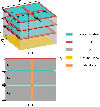
The structure proposed in this paper, as depicted in Figs. 1 (a) and (b), comprise three-layer resistive films with different sheet resistance. (R= R= 400 , R= 150 ). The resistive films are printed on a polyethylene terephthalate (PET) substrate with a permittivity of 3.7. Each layer of resistive films is supported by polymethacrylimide (PMI) foam of different thicknesses with a permittivity of 1.05. The bottom layer is a metallic plate. A metallic via runs through the center of the absorber and contact with the metallicground.
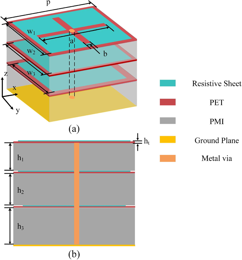
Figure 1: (a) The structure of the proposed absorber (unit cell dimension: p = 13 mm, w= w= 12 mm, w= 11 mm, a = 10 mm, b = 1 mm, h= h= 3 mm, h= 4 mm, h= 0.175 mm); (b) side view of the unit cell.
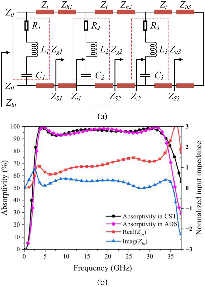
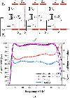
Figure 2: (a) Equivalent circuit model diagram; (b) absorptivity of CST microwave studio, ADS, and normalized input impedance of absorber.
A. Equivalent circuit analysis of the absorber without vias
The proposed absorber’s equivalent circuit model is depicted in Fig. 2 (a). The resistive films can be equivalent to RLC series circuits, The capacitance C is due to the edge length of the accumulated charge of the resistive films, and the inductance L is due to the area of the resistive films, where and and is the gap capacitance of the periodic patch. is the sheet resistance of the resistive films, is the thickness of the resistive films, and is the area of the resistive films [19, 20]. The dielectric substrate is equivalent to a transmission line. According to transmission line theory and reference [21, 22], the absorber’s input impedance can be described as follows:
| (1) |
| (2) |
| (3) |
| (4) |
| (5) |
where and are the relative permittivity of PET and PMI foam substrates. is free space impedance. The equivalent circuit model is established in the Advanced Design System (ADS), and Fig. 2 (b) presents a comparison of the simulation results obtained from ADS and CST Microwave Studio. In the frequency range of 3.2-35 GHz, the absorptivity surpasses 90% at vertical incidence. According to the normalized impedance curve in Fig. 2 (b), it is observed that the real part of the normalized input impedance is approximately 1, and the imaginary part is nearly 0. Hence, the input impedance of the absorber matches well with the impedance of the free space, leading to the achievement of broadband absorption by the absorber.
B. Performance of oblique incidence
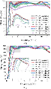
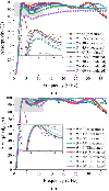
As demonstrated by Fig. 3 (a), the absorptivity persists at approximately 90% for the TE polarization angle of incidence ranging from 0 to 45. As the incident angle rises to 60, the absorption declines to about80%.
Figure 3 (b) shows that under TM polarization oblique incidence, the absorptivity remains essentially unchanged as the incident angle increases. However, the absorption bandwidth shifts to higher frequencies. When the incidence angle is 60, the displacement is 8 GHz as against vertical incidence. To examine the actual performance of the absorber and the effect of the angle of incidence on the absorption performance, we fabricated a 299299 mm sample with 2323 cells, and the resistive film was printed on a PET substrate using screen-printing technique, with each layer separated by PMI foam (Fig. 4 (b)). The sample was measured in a microwave anechoic chamber in which two sets of horn antennas (2-18 GHz, 12080 mm) were connected to two ports of a vector network analyzer (VNA) as transmitter and receiver. Respectively, the two sets of horn antennas were placed on a semi-circular track with a radius of 2 mcentered on the sample (Fig. 4 (a)). The antennas were moved on the semicircle to change the angle between the antennas and the sample during the measurement to achieve simulated oblique incidence. To ensure accurate measurement results for subsequent samples, we first measured the reflection coefficient of a metal plate of the same size as the sample. Owing to the restrictions imposed by our experimental conditions, we then measured the sample’s absorptivity at an oblique incidence angle of 0-45 in the frequency range of 2-18 GHz. The measured absorbance of the samples in this range was consistent with the simulation results. The disparity between the measurement and simulation results is predominantly ascribed to errors in sample preparation and the measurement environment.
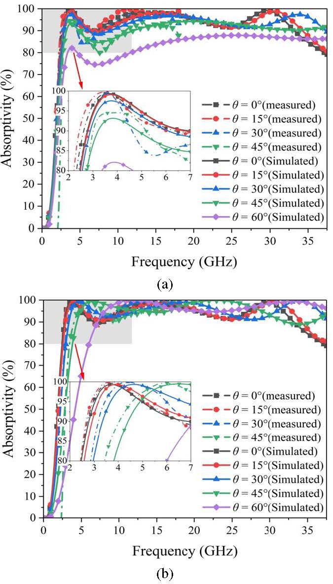
Figure 3: Absorptivity at different polarizations at oblique incidence without vias: (a) Simulation of TE polarization; (b) simulation of TM polarization.
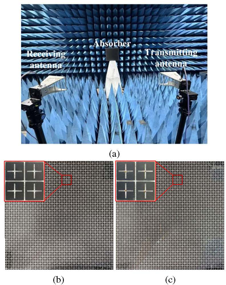
Figure 4: (a) Measurement environment of the proposed absorber; (b) top views of the proposed absorber without vias (299299 mm sample with 2323 cells); (c) top views of the proposed absorber with vias (299299 mm sample with 2323 cells).
When TM polarization is incident obliquely, the absorption bandwidth shift occurs. This is due to the change in the equivalent impedance of the substrate as the angle of incidence increases, which causes the input impedance of the absorber to change, resulting in a mismatch with the free-space impedance.
To address this issue, a metallic via is inserted in the center of the absorber unit structure. Then the substrate layer can be considered as a multi-conductor transmission line [23]. From the perspective of the incident point, the input impedance of each layer is the parallel combination of the resistive film and substrate’s impedance. The input impedance of the absorber is a parallel combination of the impedances of the individual layers, so we will analyze a single layer as an example.
There are two eigenwave modes of TM-polarized incident waves in the substrates [24]. One of the eigenmodes is the TM mode propagating in the medium, which attenuates dramatically and has a negligible effect [25]. The other type of eigenmode is the TEM wave that propagates in the multi-conductor line. Its propagation factor can be decomposed into two components: One is vertical to the resistive film and the other is parallel to it. The vertical component is equal to the wavenumber propagating in the substrate, while the parallel component is the tangential component of the incident wavenumber. And because the diameter of the metallic vias is very small, the electrical polarization on the cross-section of the conductor is also very small. Additionally, due to the principle of electromagnetic wave duality, the magnetic field on the conductor remains relatively constant, so the wave impedance is basically the same as the case of no vias.
Therefore, at any incident angle, the equivalent impedance of the substrate , as seen from the polarized incident wave of TM, is the same as that of the TEM transmission line. The length of the TEM transmission line is equal to the thickness of the absorber. This implies that remains independent of the incident angle:
| (6) |
When TM polarization oblique incidence, the input impedance of the absorber is :
| (7) |
Because the impedance of resistive films does not depend on the angle of incidence but on the characteristics of the resistive film itself, the input impedance of the absorber is not affected by the incident angle, regardless of the angle of incidence. Moreover, the resonant frequency also remains constant. Additionally, as the electric field component of the TE polarization is vertical to the metallic vias, no induced current is generated on the metallic vias. Therefore, the metallic vias do not affect the TE polarization oblique incidence.
For TE-polarised oblique incidence, the wave impedances under the two polarisations behave differently (, where is incident angle). This results in a different impedance match between the absorber and the free space under the two polarisations at the same incidence angle. For TE-incidence waves, the impedance match worsens throughout the absorbing band as the angle increases.
III. PERFORMANCE OF THE ABSORBER WITH VIAS
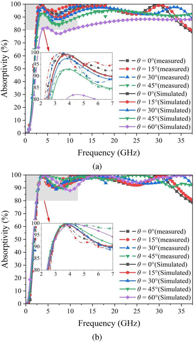
Figure 5: Absorptivity at different polarizations at oblique incidence with vias: (a) Simulation of TE polarization; (b) simulation of TM polarization.
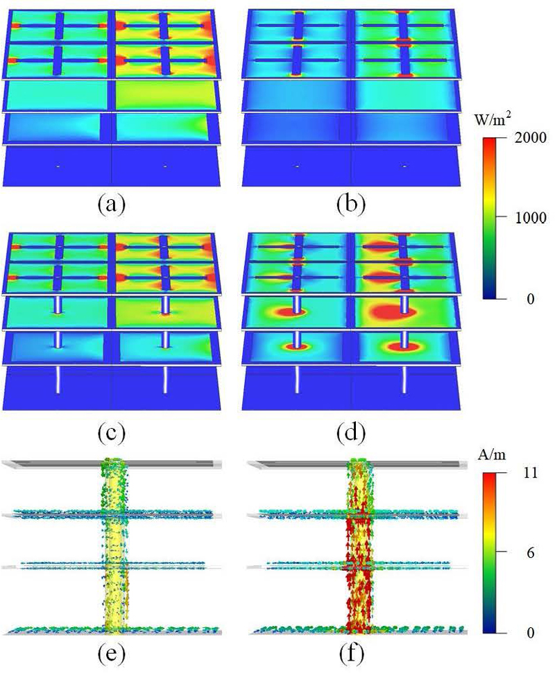
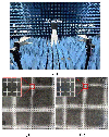
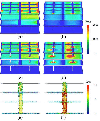
Figure 6: Surface power loss diagram at 4 GHz at 60 oblique incidence with and without vias. (a) TE polarization without vias, (b) TM polarization without vias. (c) TE polarization with vias. (d) TM polarization with vias. Surface current at 4GHz at 60 oblique incidence with vias. (e) TE polarization. (f) TMpolarization.
Table 1: Comparison of the proposed absorber with other broadband absorbers
| Ref | FBW | Thickness | Absorption for Oblique Incidences | |
| TE | TM | |||
| [6] | (4.73-39.04GHz)156% | 9.5 mm 0.17 | 80% at 45 | 90% at 45 |
| [9] | (3.87-14.84GHz)117% | 6.2 mm 0.19 | 80% at 45 | 90% at 50 |
| [26] | (3.65-13.93GHz)117% | 8 mm 0.10 | 80% at 50 | 80% at 60 |
| [27] | (2.98-16.62GHz)139% | 9.1 mm 0.13 | 80% at 45 | 90% at 45 |
| [28] | (2.05-8.3GHz)120% | 11 mm 0.19 | 80% at 45 | 80% at 45 |
| This Work | (3.2-35.5GHz)167% | 10.5 mm 0.09 | 80% at 60 | 90% at 60 |
Figure 5 (a) illustrates that under TE polarization oblique incidence, the absorptivity remains above 90% up to an angle of 45. At 60 incident angle, the absorptivity decreases to approximately 80%. The absorption effect of TE polarization oblique incidence remains essentially unchanged, indicating that vias have no effect on TE polarization. It can be seen from Fig. 5 (b) that the absorber remains angularly stable, exhibiting no shift in the absorption band at TM polarization oblique incident angle of up to 60 while retaining approximately 90% absorptivity. Figure 4 (c) displays a sample (299299 mm with 2323 cells) of the absorber for measurement purposes, and the comparison of simulated and measured results, shown in Figs. 5 (a) and (b), exhibit satisfactory agreement.
To gain a more intuitive understanding of the role of metallic vias, the power loss and surface current at 4 GHz were monitored before and after the improvement of the absorber at 60 oblique incidence. As shown in Figs. 6 (a)-(d), upon the incorporation of metallic vias, the TM polarization causes significant losses on the second and third resistive films that have direct contact with the metallic vias. On the other hand, the performance of TE polarization oblique incidence stays unaltered. Additionally, as revealed in Figs. 6 (e) and (f), the TM polarization oblique incidence prompts greater induced current on the vias, relative to the TE polarization oblique incidence. In cases of oblique incidence, the TM polarization wave can be guided through the vias, and loss on the resistive films, resulting in a reduction in the impact of the angle of incidence.
Table 1 presents a comparative analysis of the proposed absorber with those developed in recent years, in terms of relative bandwidth, thickness, and absorptivity at oblique incidence. It reveals that the proposed absorber has a wider fractional bandwidth, thinner thickness, and more stable oblique incidence performance than other absorbers.
FBW=, where is the highest frequency, is the lowest frequency.
IV. CONCLUSION
In summary, this paper presents a design of an ultra-wideband absorber that utilizes a three-layer resistive film structure. The absorber achieves over 90% absorptivity in the range of 3.2-35.5GHz, across the C, X, Ku, K, and Ka frequency bands, with a fractional bandwidth of 167%. Additionally, the absorbers exhibit good absorption for both TE and TM polarized waves in the 0-60 incident angle range. Further analysis was conducted on the impact of metallic vias using surface currents and surface power losses. Furthermore, the measurement results align well with the simulation results, demonstrating the effectiveness of the design scheme proposed in this paper. The proposed absorber has good angular stability and absorption bandwidth and shows a potential idea for stealth applications.
ACKNOWLEDGMENT
This work is supported by the National Natural Science Foundation of China under Grant No. 51507176 and No. 62201575.
REFERENCES
[1] V. G. Veselago, “The electrodynamics of substances with simultaneously negative values of and ,” Sov. Phys. Usp, vol. 10, pp. 509-514, Jan. 1968.
[2] D. R. Smith, W. J. Padilla, D. C. Vier, S. C. Nemat-Nasser, and S. Schultz, “Composite medium with simultaneously negative permeability and permittivity,” Phys. Rev. Lett., vol. 84, no. 18, pp. 4184-4187, May 2000.
[3] D. R. Smith, D. C. Vier, T. Koschny, and C. M. Soukoulis, “Electromagnetic parameter retrieval from inhomogeneous metamaterials,” Phys. Rev. E, vol. 71, no. 3, Art. no. 036617, 2005.
[4] D. R. Smith, S. Schultz, P. Markoš, and C. M. Soukoulis, “Determination of effective permittivity and permeability of metamaterials from reflection and transmission coefficients,” Phys. Rev. B, Condens. Matter, vol. 65, no. 19, Art. no. 195104,Apr. 2002.
[5] C. Liang, X. Kong, F. Wang, R. Xu, Y. Fu, X. Pang, S. Zhang, X. Shen, and L. Zhao, “A broadband perfect metamaterial absorber with angle-insensitive characteristics,” J. Electromagn. Wave Appl., vol. 37, no. 3, pp. 401-410, Mar. 2023.
[6] P. Chen, X. Kong, J. Han, W. Wang, K. Han, H. Ma, L. Zhao, and X. Shen, “Wide-angle ultra-broadband metamaterial absorber with polarization insensitive characteristics,” Chinese Phys. Lett., vol. 38, no. 2, p. 27801, Jan. 2021.
[7] R. Araneo and S. Celozzi, “Optimal design of electromagnetic absorbers,” Applied Computational Electromagnetic Society (ACES) Journal, vol. 29, no. 4, pp. 316-327, Apr. 2014.
[8] P. Zhou, Q. Huang, L. Ji, and X. Shi, “Design of a thin broadband metamaterial absorber based on resistance frequency selective surface,” Applied Computational Electromagnetic Society (ACES) Journal, vol. 34, no. 10, pp. 1494-1499,Oct. 2019.
[9] Lim and S. Lim, “Ultrawideband electromagnetic absorber using sandwiched broadband metasurfaces,” IEEE Antennas Wireless Propag. Lett., vol. 18, pp. 1887-1891, 2019.
[10] X. Lu, J. Chen, Y. Huang, Z. Wu, and A. Zhang, “Design of ultra-wideband and transparent absorber based on resistive films,” Applied Computational Electromagnetic Society (ACES) Journal, vol. 34, no. 05, pp. 765-770, May 2019.
[11] D. Wang, K. Xu, S. Luo, Y. Cui, L. Zhang, and J. Cui, “A high Q-factor dual-band terahertz metamaterial absorber and its sensing characteristics,” Nanoscale., vol. 15, no. 7, pp. 3398-3407, Feb. 2023.
[12] M. B. Ghandehari, N. Feiz, and M. Alipoor, “Circuit model analysis of a polarization and wide angle independent hexagonal shaped metamaterial absorber,” Applied Computational Electromagnetic Society (ACES) Journal, vol. 30, no. 8, pp. 909-914, Aug. 2015.
[13] F. Dincer, M. Karaaslan, E. Unal, O. Akgol, and C. Sabah, “Multi-band metamaterial absorber: design, experiment and physical interpretation,” Applied Computational Electromagnetic Society (ACES) Journal, vol. 29, no. 3, pp. 197-202,Mar. 2014.
[14] T. Deng, Z. W. Li, and Z. N. Chen, “Ultrathin broadband absorber using frequency-selective surface and frequency-dispersive magnetic materials,” IEEE Trans. Antennas Propag., vol. 65, no. 11, pp. 5886-5894, Nov. 2017.
[15] H. Xiong, J. S. Hong, C.-M. Luo, and L. L. Zhong, “An ultrathin and broadband metamaterial absorber using multi-layer structures,” J. Appl. Phys., vol. 114, no. 6, Art. no. 064109, Aug. 2013.
[16] J. Yu, W. Jiang, and S. Gong, “Wideband angular stable absorber based on spoof surface plasmon polariton for RCS reduction,” IEEE Antennas Wireless Propag. Lett., vol. 19, no. 7, pp. 1058-1062, July 2020.
[17] Z. C. Lin, Y. Zhang, L. Li, Y. T. Zhao, J. Chen, and K. D. Xu, “Extremely wideband metamaterial absorber using spatial lossy transmission lines and resistively loaded high impedance surface,” IEEE Trans. Microwave Theory Tech., vol. 71, no. 8, pp. 3323-3332, Aug. 2023.
[18] B. Zhang and K.-D. Xu, “Dynamically switchable terahertz absorber based on a hybrid metamaterial with vanadium dioxide and graphene,” J. Opt. Soc. Amer. B Opt. Phys., vol. 38, no. 11, pp. 3425, Nov. 2021.
[19] F. Costa, A. Monorchio, and G. Manara, “Analysis and design of ultrathin electromagnetic absorbers comprising resistively loaded high impedance surfaces,” IEEE Trans. Antennas Propag., vol. 58, no. 5, pp. 1551-1558, May 2010.
[20] F. Costa, A. Monorchio, and G. Manara, “An equivalent circuit model of frequency selective surfaces embedded within dielectric layers,” Proc. IEEE Antennas Propag. Soc. Int. Symp., pp. 1-4,2009.
[21] Q. Zhou, X. W. Yin, F. Ye, R. Mo, Z. M. Tang, L. F. Cheng, and L. T. Zhang, “Optically transparent and flexible broadband microwave metamaterial absorber with sandwich structure,” Appl. Phys. A, vol. 125, no. 2, Art. no. 131, 2019.
[22] L. Sun, H. Cheng, Y. Zhou, and J. Wang, “Broadband metamaterial absorber based on coupling resistive frequency selective surface,” Opt. Exp., vol. 20, no. 4, pp. 4675-4680, Feb. 2012.
[23] R. E. Diaz, J. T. Aberle, and W. E. McKinzie, “TM mode analysis of a Sievenpiper high-impedance reactive surface,” in Proc. IEEE Antennas Propag. Symp., pp. 327-330, 2000.
[24] C. R. Simovski, S. A. Tretyakov, and P. de Maagt, “Artificial high impedance-surfaces: Analytical theory for oblique incidence,” Proc. Antennas Propag. Soc. Int. Symp., vol. 4, pp. 434-437, 2003.
[25] S. I. Maslovski, S. A. Tretyakov, and P. A. Belov, “Wire media with negative effective permittivity: A quasistatic model,” Microw. Opt. Technol. Lett., vol. 35, no. 1, pp. 47-51, Oct. 2002.
[26] J. F. Chen, Z. Y. Hu, G. D. Wang, X. T. Huang, S. M. Wang, X. W. Hu, and M. H. Liu, “High-impedance surface-based broadband absorbers with interference theory,” IEEE Trans. Antennas Propag., vol. 63, no. 10, pp. 4367-4374, Oct. 2015.
[27] J. F. Wei, Y. He, S.W. Bie, S. Wu, Z. P. Lei, W. Deng, Y. T. Liu, Y. L. Zhang, C. L. Li, J. Q. Ai, and J. J. Jiang, “Flexible design and realization of wideband microwave absorber with double-layered resistor loaded FSS,” J. Phys. D, Appl. Phys., vol. 52, no. 18, Art. no. 185101, May 2019.
[28] Y. Chang and Yung L. Chow, “Broadband microwave absorber based on end-loading folded-dipole array,” Applied Computational Electromagnetic Society (ACES) Journal, vol. 34, no. 9, pp. 1327-1333, Sep. 2019.
BIOGRAPHIES

Ruofeng Xu received the B.Sc. (2004) degree from Suzhou University in electronics and science and technology and the M.Sc. (2006) and Ph.D. (2010) degrees in electronic engineering from the University of Kent, UK. He was the visiting scholar (2018) for one year in Rutgers University, USA. Now he has been a lecturer in School of Information and Control Engineering, China University of Mining and Technology. His main research directions are microwave technology and application.

Xingyu Ma has been a masters student at the School of Information and Control Engineering, China University of Mining and Technology. His main researches are on microwave absorbers, frequency select surfaces, etc.

Xianglin Kong has a doctoral degree in Information and Control Engineering at China University of Mining and Technology. His main research interests include metamaterial absorbers and encoded metasurfaces.

Shengjun Zhang has been a researcher at Laboratory of Experimental Physics and Computational Mathematics. His main research directions are on electromagnetic waves technologies, etc.

Jiaqi Liu has been a researcher at Laboratory of Experimental Physics and Computational Mathematics. His main research directions are on electromagnetic waves technologies, etc.

Lei Zhao has been a professor and doctoral supervisor in School of Information and Control Engineering, China University of Mining and Technology. He has been a senior member of IEEE, member of the Antenna Branch of the China Electronics Society, and chairman of IEEE AP-S Chapter Xuzhou. His main researches are on RF microwave devices, new electromagnetic materials, vortex wave communication, computational electromagnetics, etc.
ACES JOURNAL, Vol. 39, No. 8, 675–682
doi: 10.13052/2024.ACES.J.390802
© 2024 River Publishers