Design of a Reconfigurable Band-notched Wideband Antenna using EBG Structures
Xiaoyan Zhang, Ziao Li, Aiyun Zhan*, and Yan Mei
School of Information Engineering
East China Jiaotong University, Nanchang, 330013, China
xy_zhang3129@ecjtu.edu.cn, lza_2017@163.com, 707290432@qq.com, 360291931@qq.com
Submitted On: November 1, 2023; Accepted On: December 15, 2023
ABSTRACT
A compact WLAN band-notched reconfigurable wideband antenna using two mushroom-like electromagnetic band-gap (EBG) structures is proposed in this paper. It is designed based on a dual wideband microstrip feed patch antenna with operating frequency bands of 2.2-3.7 GHz and 4.8-6 GHz. One of the EBG cells is positioned alongside the feed line, while the other EBG cell is laid on the back of the substrate. The patch or ground of the two EBG units are fed with a stronger current through a ground slot and a parasitic stub respectively, and the connections between the EBG structures and the antenna are controlled by loading a PIN diode with two 56 pF DC blocking capacitors. The advantage of this proposed design is that the antenna and the EBG unit can be designed independently. The proposed antenna has an overall size of 35461.6 mm. When testing the S of the antenna, the influence of the bias circuit on the antenna is also considered. The measured results show that the proposed antenna can generate two notched bands of 2.3-2.49 GHz and 5.11-5.51 GHz of WLAN, and the realized gain in the notch bands can be reduced to -2.65 dBi and -4.55 dBi, respectively, demonstrating its anti-interference characteristics, and can be applied in band notch broadband communication systems or anti-interference communication equipments such as unmanned aerial vehicles and radars.
Keywords: Anti-interference, electromagnetic band-gap (EBG), PIN diodes, reconfigurable band notched antenna, WLAN.
I. INTRODUCTION
The frequency bands of WLAN (2.4-2.4835 GHz, 5.15-5.825 GHz) are widely used in wireless communication systems. In order to prevent its interference, some wideband antennas need to own a single or a dual band-rejected filtering characteristic in the WLAN band. The main approaches used by these researches can be mainly divided into two categories [1]. The first category is to generate radiation perturbation through etching slots on the ground/ patches or loading parasitic stubs [2, 3] and stepped impedance resonators [1, 4] on the patches. The disadvantage of these methods is that they will change the radiation pattern of the antenna itself [1]. Moreover, due to the limited area that can be cleared, it is hard to load switch components on the patches, making it difficult to achieve reconfigurable band notch design. The second category is to integrate filters at the feed port of the antennas to reject the interfering sources [5–6]. By controlling the filters or their connections, the notch band can be tuned. While the filters increase the complexity of antenna design. In [7–8], the methods of adding an open loop resonator near to a feed line were proposed, which can generate a stopband in the signal source through coupling resonance. Although the frequency band can be adjusted by changing the on-off state of the resonator, its coupling effect is difficult toeliminate [9].
In recent years, electromagnetic band-gap (EBG) technology has been introduced into the single-, dual-, and multi-band-rejected antennas design [10–14] In these studies, the EBGs are mainly divided into two types: uniplanar EBG [10, 11] and high impedance electromagnetic surface (HIS) [12–15]. For example, two spiral uniplanar EBGs are symmetrically placed on both sides of a dual notch antenna’s feed line in [10], and asymmetrically placed on the upper and lower sides of the microstrip feed line in [11], resulting in two additional notch bands; simpler structures of conventional mushroom-type HIS-EBG (CMT-HIS-EBG) [1, 12] or edge-located vias HIS-EBG (ELV-HIS-EBG) [12–15] were placed next to or in the middle of the antenna feed line [14], or even on the back of the antenna (with the patch as the ground) [15] to create the notch bands. The principle of loading uniplanar EBG is similar to the methods of positioning resonators next to the feed line, so the same problem is faced when realizing notch reconfigurability. In contrast, the essence of using HIS-EBG to design band-notched antennas belongs to the second category, as the HIS-EBG unit has a bandstop property, so it can be used as a bandstop filter without affecting the behavior of the antenna itself.
Based on the above reasons, the design of reconfigurable band-notched antennas using HIS-EBG structures has attracted research interest [16–18]. For example, in 2015, the concept of six band-notched reconfigurable antenna using six ELV-HIS-EBG units was proposed, but the bias circuit was not considered in this design. Therefore, the EBG units and the switches were printed separately in an intermediate layer and placed underneath the transmission line of the antenna [16]; in 2016, the copper strips of two ELV-HIS-EBGs are connected with a PIN diode, achieving a single reconfigurable band-rejected function, but its realized gain in the notch band at 4 GHz is about -1.5 dBi, which is not significantly decreased [17]; In 2020, two CMT-HIS-EBGs are surrounded by a square copper ring and connected to the ring using a varactor diode. By controlling the ON/OFF state of the varactor diodes, the reconfigurability in the notch band of 5.3 GHz was realized. However, the gain in the rejected band only reaches 0 dBi [18].
The patch of the HIS-EBG is connected to the ground through punching a copper via into the substrate, forming a complete circuit. The challenge of designing HIS-EBG-based band-notched reconfigurable antennas is that the PIN diodes cannot be directly loaded on the vias to control the ON/OFF of the circuit. In addition, the electronic components of the switches will occupy a certain clearance area, leading to changes in the antenna structure.
In this paper, a novel WLAN band-notched reconfigurable wideband monopole antenna based on two HIS-EBG was designed, fabricated, and tested. The impact of switches (it is composed of a PIN diode and two capacitors) on antenna performance is considered in testing. The switches are not directly loaded in the EBG unit but are loaded in its ground slot and the parasitic stubs. By extending the parasitic stubs and the ground slots into the areas with stronger currents, more surface waves will be directed into the EBG unit. The proposed method can enable the antenna and the HIS-EBG unit to be designed independently, and can sharply decrease the gain within the notch band, providing a new approach for the design of band-notched reconfigurable antennas.
II. DESIGN CONFIGURATION AND APPROACH
A. Overall design of the antenna
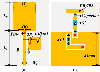
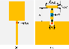
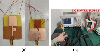
To verify the design scheme, a square microstrip patch antenna is used as the basic structure. It is fabricated on a FR4 substrate, with a dielectric constant of 4.4 and a loss tangent of 0.02. The prototype of the proposed antenna is shown in Fig. 1. As shown in Fig. 1 (a), the overall size of the antenna is 35460.8 mm, and the parameters of the patch antenna are L = 22 mm, W = 16 mm, L = 26.4 mm, and W =2 mm.
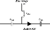
Two square patch mushroom-like HIS-EBG units EBG #1 and EBG #2 are placed on the right side of the microstrip line (see Fig. 1 (a)) and on the back of the patch (see Fig. 1 (b)), fully utilizing the available space of the antenna. The connections between the EBGs and the patch antenna are controlled by two RF switches (represented as S1 and S2). These switches are composed of a BAR50-02V PIN diode and two C = 56 pF DC blocking capacitors. Figure 2 shows the equivalent bias circuit for the antenna. The bias voltage is 1 V, and a L = 51 nH inductor is used to stabilize the bias current.
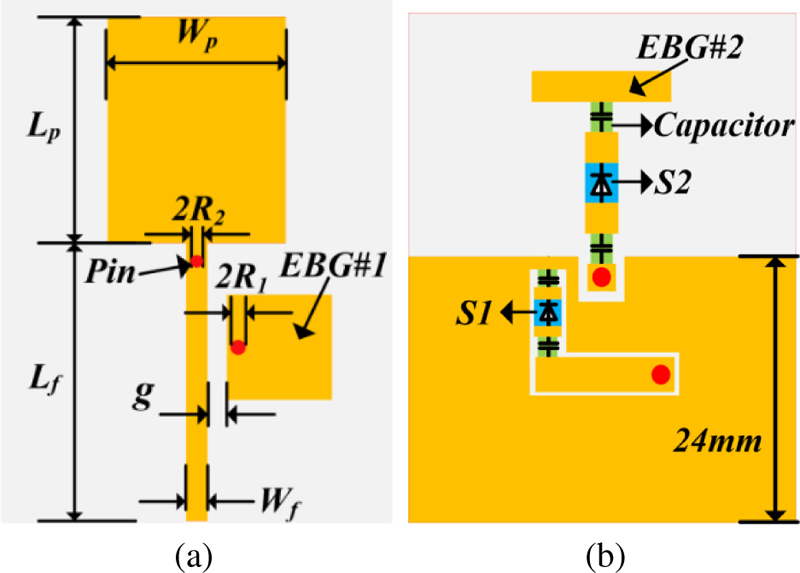
Figure 1: Geometry of the proposed antenna includes (a) top view and (b) bottom view.
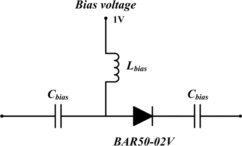
Figure 2: Antenna bias circuit.
B. Antenna design by loading EBG #1
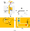
As Fig. 3 (a) shows, a microstrip-line-based method [12] is used to study the stopband characteristics of the EBG #1. Specifically, without considering the radiator of the patch antenna, the EBG #1 is placed on the right side of the microstrip line with a distance of g.
The equivalent circuit of this model is shown in Fig. 3 (b). C is the fringing capacitance between the EBG #1 and the microstrip line, C and L are the capacitance and inductance generated by the mushroom-shaped EBG #1 itself. They are simply estimated using the formula [19] for estimating periodic EBG parameters as
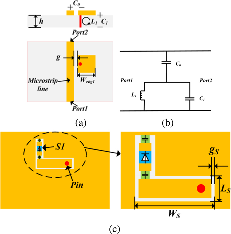
Figure 3: Microstrip-line-based model: (a) Configuration diagram, (b) equivalent circuit model, (c) back view of the circuit.
| (1) | |
| (2) | |
| (3) |
where Wis the width of the patch for the square EBG #1 cell,= 4.4, is the relative dielectric constant of FR4, and h = 0.8 mm is the thickness of the substrate. Usually, g is much smaller than W, so C is mainly influenced by W.
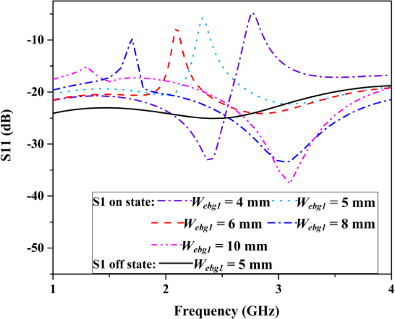
Figure 4: S changes of the patch antenna with or without EBG #1 at different W.
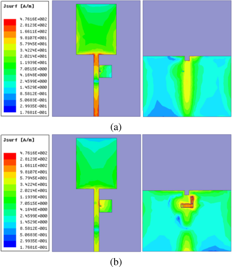
Figure 5: The current distribution on the back of the antenna before and after etching the L-shaped slot at a resonant frequency of 2.45 GHz: (a) before grooving and (b) after grooving.
The resonant frequency(f) of this model can be derived as
| (4) |
Obviously, once g is fixed, the approximate value of W can be inferred from the selected band-notch frequency f. Therefore, further optimization can be carried out based on this value. During this process, g can be determined simultaneously.
Figure 3 (c) shows the back of the model. It can be seen that an L-shaped slot has been etched on the ground around the pin of EBG #1, which separates the connection between the EBG #1 and the ground, preventing the EBG #1 from forming a complete circuit. Then, a BAR50-02V PIN diode and two DC blocking capacitors are embedded at the end of the slot, so the connection state between the EBG #1 and the microstrip line can be controlled by controlling the ON/OFF state of S1. Due to the extended length of the L-shaped slot being much longer than the width of the slot, it allows sufficient area for the loading of diodes and capacitors. In addition, by controlling the extension direction of the slot, the amount of current fed into the EBG #1 can be controlled.
In order to observe the effect of W on the microstrip line’s reflection, the state of S1 is set to ON with g = 0.2 mm. According to Eq. (4), the Wcorresponding to 2.45 GHz is predicted to be approximately 8 mm. Therefore, the scanning range of W is selected to be 4-10 mm. As shown in Fig. 4, when W = 5 mm, the antenna can generate the rejected frequency of 2.45 GHz. Due to the neglect of edge effects in formulas (1) and (2), the estimated Wis larger than the actual one. Then, the state of S1 is switched to OFF to observe whether the EBG #1 is still coupled to the microstrip line when the circuit is open. Obviously, in this case, the impact of EBG #1 can be ignored.
Figures 5 (a) and (b) compare the current distribution on the back of the antenna before and after etching the L-shaped slot. It can be observed that as the current converges toward the L-shaped slot, it does indeed serve to guide the current.
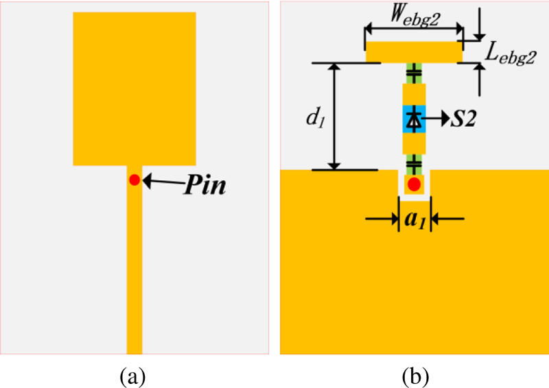
Figure 6: The structural diagram of the antenna loaded EBG #2 from (a) top view and (b) back view.
C. Antenna design by loading EBG #2
Considering that the EBG cell needs to be coupled with sufficient current to better achieve frequency rejecting, it is hard to achieve high-frequency of WLAN filtering by reducing the size of the EBG # 1 further. And it is necessary to consider the welding interval and difficulty issues between the processed SMA connector and EBG and capacitor components. Therefore, the EBG # 2 is placed on the back of the antenna patch, as shown in Fig. 6. It is connected to the feeder through S2 and uses the conductivity of the microstrip line as a ground.
Figure 7 shows the effect of EBG #2 size parameters W and L (with d = 2.8 mm and a = 1.8 mm) on the antenna’s notch frequency. When L = 0.5 mm, it can be observed that the filtered frequency will shift toward lower frequencies as W increases. A similar phenomenon also occurs when L increases. When S2 is in the OFF state, it can be seen that the antenna operates in the high-frequency range of 4.2-5.76 GHz. Like the EBG #1, the EBG #2 will not interfere with the operation of the antenna itself in thisstate.
Figure 8 shows the influence of don the S of the monopole antenna with EBG #2. It can be observed that when d increases from 2.8 mm to 3.2 mm, the center frequency of the notch band decreases from 5.15 GHz to 5 GHz, with a slight change, indicating that d has little effect on the antenna.
The optimized parameters are shown in Table 1.
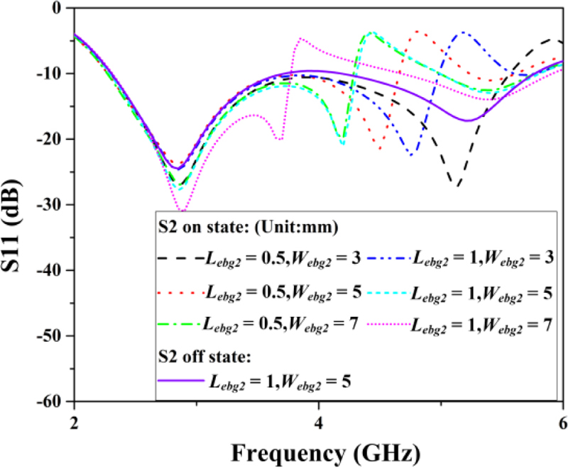
Figure 7: S changes of the patch antenna with or without EBG #2 at different Wand L.
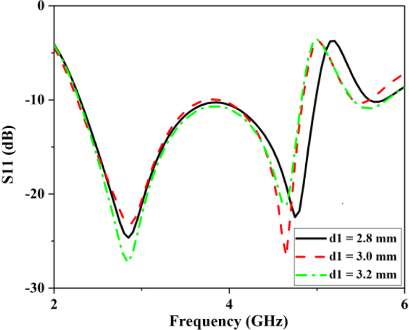
Figure 8: S of the patch antenna with EBG #2 at different d.
Table 1: Optimized parameters of the EBG units (unit: mm)
| Parameter | Value | Parameter | Value |
|---|---|---|---|
| W | 5 | a | 1.8 |
| W | 3 | R | 0.25 |
| L | 1 | R | 0.3 |
| g | 0.1 | L | 1.45 |
| W | 4.9 | d | 2.8 |
For convenience, the different state combinations of S1 and S2 are represented by F1, F2, and F3, which are listed in Table 2.
Table 2: Symbols of switches in different states
| Symbols | Diode Status | |
|---|---|---|
| S1 | S2 | |
| F1 | OFF | OFF |
| F2 | OFF | ON |
| F3 | ON | OFF |
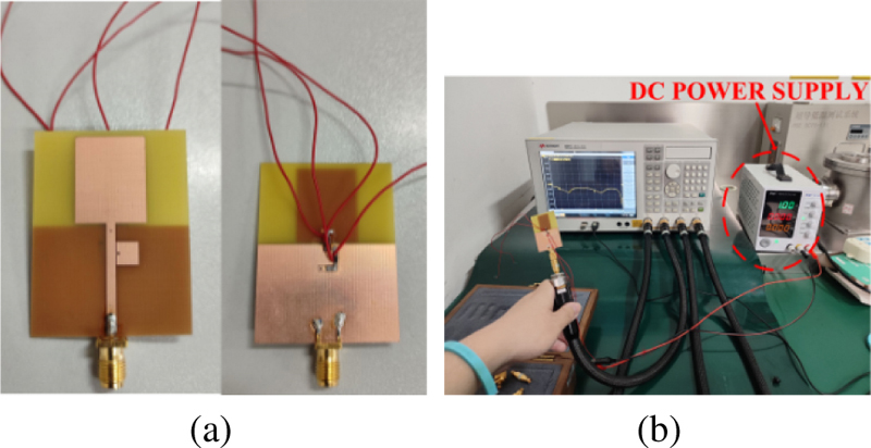
Figure 9: Photograph of the fabricated antenna: (a) Physical photos of the antenna and (b) photos of the testing environment.
III. MEASURED RESULTS AND DISCUSSION
The proposed antenna is fabricated and measured as shown in Fig. 9. Considering that DC regulated power supply is an existing equipment in the laboratory, it has the function of a switching power supply and can provide stable and adjustable voltage. Therefore, for ease of testing, we use DC instead of batteries to power the bias circuit. Due to the fact that the diodes of the proposed antenna will not be in the ON-ON states in the experiment, only one DC is needed to power two PIN diodes separately to test the performance of the antenna in three states. When testing S, a 1 V stabilized power supply was connected to the bias circuit of the antenna, so the impact of the bias circuit on the antenna performance was tested.
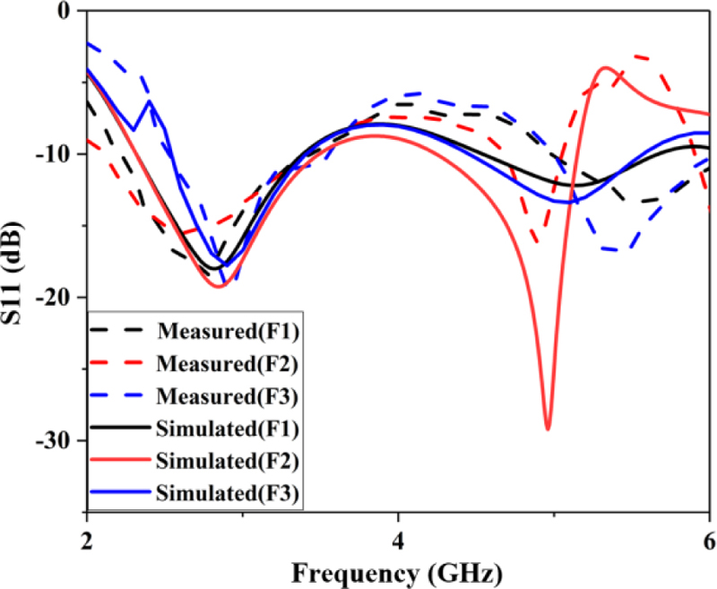
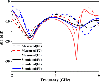
Figure 10: Comparisons between the simulated and measured S of the proposed antenna in different switching states.
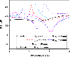
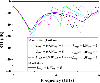
The comparisons of the simulated and measured Sin F1, F2, and F3 states are shown in Fig. 10. The measured results show that in F1 state (the diodes in OFF-OFF state), the antenna operates in two frequency bands: 2.2-3.7 GHz and 4.8-6 GHz; In F2 state, the antenna can generate a notch band of 5.11-5.51 GHz, which belongs to the high-frequency of the WLAN; In F3 state, the antenna can generate a notch of 2.3-2.49 GHz, covering the low-frequency of the WLAN. Although there are some differences between the simulation and test results, which may be due to the fabrication tolerance and welding of the switch, they are generally consistent.
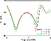
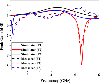
The simulated and measured peak gains of the antenna in different switching states are shown in Fig. 11. It can be seen that the low-frequency peak gain and high-frequency peak gain of the antenna in F1 state are 2.5 dBi and 3.3 dBi, respectively. The gain of the antenna within the two WLAN filtering frequencies is as low as -2.65 dBi and -4.65 dBi, respectively, indicating that the antenna can effectively suppress the gain in the notch frequency bands.
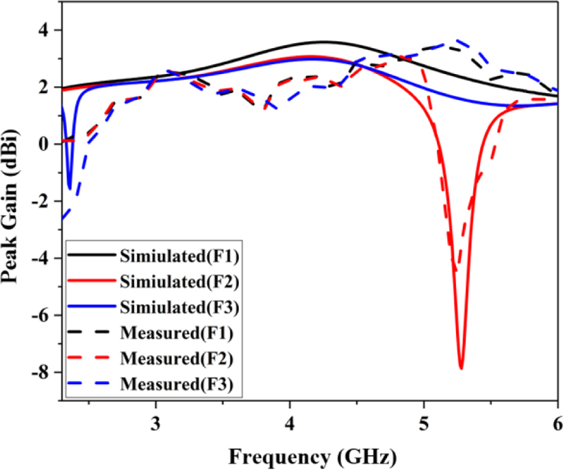
Figure 11: Comparisons between the simulated and measured peak gains of the proposed antenna in different switching states.
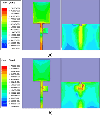
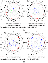
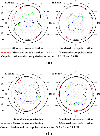
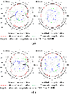
Figures 12, 13, and 14 show the two-dimensional radiation patterns of the proposed antenna at resonance frequencies of 2.8 GHz and 5.25 GHz, 2.8 GHz and 4.8 GHz, and 2.8 GHz and 5.25 GHz in different switching states. In these three states, the co-polarization and cross-polarization ratios exceed 21 dB, 27 dB, and 21 dB, respectively. As the figures show, the omnidirectional radiation characteristics are observed in the E and H planes.
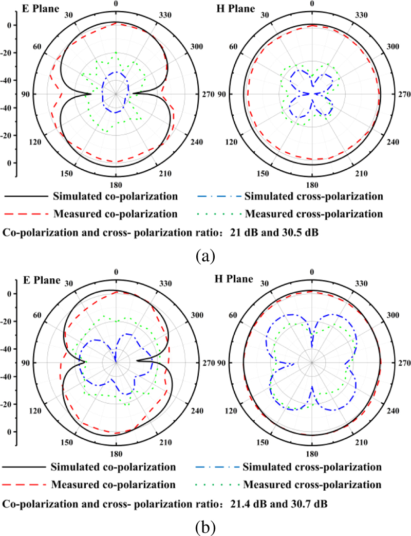
Figure 12: Simulated and measured radiation patterns at frequencies of (a) 2.8 GHz (with status F1) and (b) 5.25 GHz (with status F1).
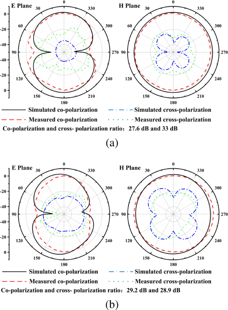
Figure 13: Simulated and measured radiation patterns at frequencies of (a) 2.8 GHz (with status F2) and (b) 4.8 GHz (with status F2).
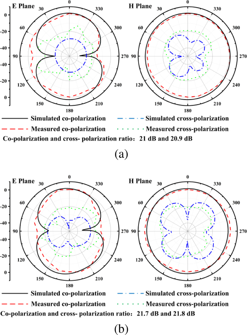
Figure 14: Simulated and measured radiation patterns at frequencies of (a) 2.8 GHz (with status F3) and (b) 5.25 GHz (with status F3).
Table 3: Comparisons with the other EBG notch-band antennas
The performance comparison between the proposed antenna and other antennas in references [15, 16, 17, 18] is listed in Table 3. The results show that the filtering frequency of the antenna covers the two frequency bands of WLAN, and has a relatively small size and low gain in the notch band, demonstrating a better performance.
IV. CONCLUSION
A dual broadband monopole antenna with a bias circuit and PIN diode based on EBG structure and a notch reconfigurable function is proposed. The two mushroom-shaped EBGs are placed at the edge of the feeder and behind the radiation patch, making full use of the available space of the antenna. By controlling the ON/OFF state of the diodes through the paranoid circuit, the band-notched reconfigurable function of the two bands can be realized. The measured results show that the proposed antenna can operate in three states: OFF–OFF, OFF–ON, and ON–ON. When PIN diodes are in the OFF–OFF states, the antenna can operate at frequencies of 2.2-3.7 GHz and 4.8-6 GHz, with a peak gain of 2.5 dBi and 3.3 dBi, respectively. When PIN diodes are in the OFF–ON states, a notched band of 5.11-5.51 GHz is generated with a realized gain as low as -4.55 dBi. When PIN diodes are in the ON–ON states, a notched band of 2.3-2.49 GHz is generated, and the realized gain of the antenna in the notched band is -2.65 dBi. This antenna is applicable for band notch broadband communication systems.
ACKNOWLEDGMENT
The authors wish to acknowledge the support of the Jiangxi Provincial Department of Education Project (GJJ2200622).
REFERENCES
[1] M. Yazdi and N. Komjani, “Design of a band-notched UWB monopole antenna by means of an EBG structure,” IEEE Antennas And Wireless Propagation Letters, vol. 10, pp. 170-173, Mar. 2011.
[2] X. Zhang, H. Xu, Y. Xie, and Q. Wu, “A dual band-notched antenna for UWB applications,” Progress in Electromagnetics Research Letters, vol. 96, pp. 105-111, Feb. 2021.
[3] J. Liu, Z. Tang, and Y. Yin, “A differential CPW-fed ultra-wideband antenna with dual notched bands,” Applied Computational Electromagnetics Society (ACES) Journal, vol. 33, no. 6, pp. 610-615, June 2018.
[4] S. Palanisamy and B. Thangaraju, “Design and analysis of clover leaf-shaped fractal antenna integrated with stepped impedance resonator for wireless applications,” International Journal of Communication Systems, vo. 35, no. 11, pp. 1-18, July 2022.
[5] C. G. Hynes and R. G. Vaughan, “Conical monopole antenna with integrated tunable notch filters,” IEEE Antennas And Wireless Propagation Letters, vol. 19, no. 12, pp. 2398-2402, Dec.2020.
[6] H. Su, L. L. Wu, Y. Zhang, J. Zhang, H. L. Xu, and X. Y. Zhang, “Circuit modeling and parameter extracting of a filtering series-fed antenna,” IEEE Transactions on Microwave Theory and Techniques, vol. 71, no. 4, pp. 1640-1653, Apr. 2023.
[7] Y. J. Guo, K. D. Xu, and X. H. Tang, “Multi-functional ultra-wideband monopole antenna with high frequency selectivity,” Applied Computational Electromagnetics Society (ACES) Journal, vol. 33, no. 1, pp. 37-42, Jan. 2018.
[8] W. A. E. Ali and A. A. Ibrahim, “Tunable band-notched UWB antenna from WLAN to WiMAX with open loop resonators using lumped capacitors,” Applied Computational Electromagnetics Society (ACES) Journal, vol. 33, no. 6, pp. 603-609, June 2018.
[9] A. V. Golliwar and M. S. Narlawar, “Multiple controllable band notch antenna for UWB cognitive radio application,” International Conference on Signal Processing and Integrated Networks, Noida, pp. 694-697, Feb. 2016.
[10] S. Peddakrishna, V. Kollipara, J. Kumar, and T. Khan, “Slot and EBG-loaded compact quad band-notched UWB antenna,” Iranian Journal of Science and Technology, Transactions of Electrical Engineering, vol. 46, pp. 205-212, Oct. 2022.
[11] S. Modak, T. Khan, and R. H. Laskar, “Penta-notched UWB monopole antenna using EBG structures and fork-shaped slots,” Radio Science, vol. 55, issue. 9, pp. 1-11, Sep. 2020.
[12] L. Peng and C. Ruan, “UWB Band-notched monopole antenna design using electromagnetic-bandgap structures,” IEEE Transactions on Microwave Theory and Techniques, vol. 59, no. 4, pp. 1074-1081, Apr. 2011.
[13] P. P. Bhavarthe, S. S. Rathod, and K. T. V. Reddy, “A compact dual band gap electromagnetic band gap structure,” IEEE Transactions on Antennas and Propagation, vol. 67, no. 1, pp. 596-600, Jan. 2019.
[14] L. Peng, B. Wen, X. Li, X. Jiang, and S. Li, “CPW fed UWB antenna by EBGs with wide rectangular notched-band,” IEEE Access, vol. 4, pp. 9545-9552, Dec. 2016.
[15] A. Abbas, N. Hussain, J. Lee, S. G. Park, and N. Kim, “Triple rectangular notch UWB antenna using EBG and SRR,” IEEE Access, vol. 9, pp. 2508-2515, Jan. 2021.
[16] H. A. Majid, A. Rahim, M. R. Hamid, N. A. Murad, N. A. Samsuri, M. F. M. Yusof, and O. Ayop, “Reconfigurable notched wideband antenna using EBG structure,” Microwave and Optical Technology Letters, vol. 57, pp. 497-501, Feb. 2015.
[17] H. A. Majid, M. K. A. Rahim, M. R. Hamid, N. A. Murad, N. A. Samsuri, M. F. M. Yusof, and M. R. Kamarudin, “Band-notched reconfigurable CPW-fed UWB antenna,” Applied Physics A, vol. 122, no. 347, pp. 1-6, Mar. 2016.
[18] A. S. Elkorany, H. A. Mohamed, Z. F. Elsharkawy, and D. A. Saleeb, “Heart shaped reconfigurable band-notched ultra-wide band antenna using electromagnetic band-gap structure and varactor diodes,” Analog Integrated Circuits and Signal Processing, vol. 105, pp. 385-393, Aug. 2020.
[19] V. R. Kapure and S. S. Rathod, “A two element EBG-inspired UWB MIMO antenna with triple band notched characteristics and high isolation,” Sadhana-Academy Proceedings in Engineering Sciences, vol. 48, no. 7, pp. 1-16, Jan. 2023.
[20] D. F. Sievenpiper, “High-impedence electromagnetics surfaces,” Ph.D. dissertation, UCLA, 1999.
BIOGRAPHIES

Xianyan Zhang received the B.S. degree in applied physics and M.S. degree in physical electronics from Yunnan University, Kunming, China, in 2001 and 2004, respectively, and the Ph.D. degree in electromagnetic field and microwave technology from Institute of Electronics, Chinese Academy of Sciences in 2007. Her research interests include electromagnetic computation, antenna design, and wireless power transmission structure design.

Ziao Li was born in 2000 in Guixi City, Jiangxi Province, China. He obtained a bachelor’s degree in engineering from the School of Science and Technology of East China Jiaotong University and is currently studying at the School of Information Engineering of East China Jiao Tong University. His main research direction is antenna design

Aiyun Zhan was born in Nantong, Jiangsu, China in 1973. She received the B.S. degree from Southwest Jiaotong University in 1997, and rhe M.S. degree in East China Jiaotong University in 2008. She is currently working at the School of Information Engineering, East China Jiaotong University. Her research interests focus on channel coding and optical communication.

Yan Mei obtained a bachelor’s degree in communication engineering from the School of Information and Communication, National Defense University of the People’s Liberation Army of China in 2002, and a master’s degree in computer science and technology from East China Jiaotong University in 2009. Research interests include wireless communication and deep learning.
ACES JOURNAL, Vol. 38, No. 11, 895–902
doi: 10.13052/2023.ACES.J.381108
© 2023 River Publishers