Butler Matrix Components Based on Substrate Integrated Waveguide Fed by Microstrip Separation Feedline for 5G Application
Yaqdhan Mahmood Hussein, Noor Asniza Murad, Mohamad Kamal A. Rahim, and Hatem Oday Hanoosh
1Advanced RF & Microwave Research Group
School of Electrical Engineering Faculty of Engineering, Universiti Teknologi Malaysia, Johor, Malaysia
mdkamal@utm.my, noorasniza@utm.my
2Department of Electronic and Communication
College of Engineering, Al Muthanna University, Al Muthanna, Iraq
yaqthanm79@gmail.com, hatem.altaee1990@gmail.com
3College of Engineering
Al Ayen University, Nasiriyah 64001, Iraq
Submitted On: September 28, 2024; Accepted On: December 10, 2024
ABSTRACT
This paper presents a beamforming component based on vias variation substrate integrated waveguide (SIW) method at Ka-band. At Ka-band, the losses are high when planar structures are implemented due to the small wavelength, beside the expected losses from the component’s losses. Therefore, SIW technology with vias manipulation is introduced. This work aims to present a low loss coupler, crossover, and phase shifter for beamforming based on SIW at 26 GHz. Coupler and crossover are designed with vias variation based on the metallic fill inside the vias microstrip separation feedline, used for input and output ports to achieve enough distance between each adjacent port, and compact design with loss phase error. The proposed designs are simulated using CST software and fabricated using Rogers 5880 substrate with thickness of 0.508 mm and permittivity of 2.2. The measured performance agreed well with the simulated results. A return loss of less than 20 dB is achieved over a bandwidth of 5 GHz. A perfect 3 dB and 0 dB are obtained at coupler and crossover outputs. The measured phase difference 88.8 is observed at the outputs. Overall, the coupler and crossover show great potential performance for Ka-band applications.
Index Terms: 5G application, beamforming, coupler, crossover, Ka-band, substrate integrated waveguide (SIW).
I. INTRODUCTION
Beamforming networks play an important role in the realizing of switched phase array systems [1–3], especially for higher bands of the fifth-generation systems toward millimeter bands. Beamforming networks aim to provide high receiving signal sensitivity toward receivers. In addition, higher bandwidth and high gain antennas and devices are needed in future beamforming networks [4]. At frequencies such as 26 and 28 GHz, the antennas and millimeter-wave devices suffer from high losses due to path loss and the technology used in their designs. Technology such as planar microstrip has loss at higher frequencies. Hence, substrate integrated waveguide (SIW) is proposed to solve these issues as SIW combines the properties of both microstrip and waveguide technology [5–8]. Couplers control the magnitude and the phase outputs of the beamforming [9, 10], whilst crossover maintains the output of the signal magnitude and the phase with no change [11, 12]. Numerous couplers and crossover topologies are designed using microstrip couplers, SIW couplers, and waveguide couplers [11, 13–17]. Hybrid couplers received significant attention [14, 15] due to their simplicity and ability to support split of power at outputs [14]. However, these couplers may suffer from high loss transmission lines and fabrication tolerance at higher frequency. In addition, implementing couplers using planar substrate produces unwanted crosstalk between output ports due to the very small distance between the coupled lines [16]. This results in high insertion loss and phase difference error at output ports. Therefore, SIW structure is proposed for designing coupler and crossover in millimeter-wave devices. SIW helps in reducing crosstalk among the outputs and increases the coupling of SIW apertures [11, 17].
In this paper, a SIW coupler and crossover are realized by vias separation with modified metal wall method at 26 GHz. The coupler and crossover are designed with a series of parallel vias and coupling vias. The designed components are simulated using CST software technology and performance is validated with measurement responses.
II. RELATED WORK
A. Coupler
Several SIW couplers (see Table 1) have been presented with different resonant frequencies in millimeter-wave bands [18, 19]. In an X-band wideband coupler utilizing SIW, the coupler exhibited a 3 GHz bandwidth and a coupling factor of 4 dB [18]. The vias (via holes) were strategically distributed around the coupling area to maximize coupling between the output ports. However, the coupler lacked validation through measurements. Additionally, the phase difference error was approximately 5. In [19], researchers presented a directional coupler operating at 15 GHz, which employed backward and forward SIW vias coupling. In [20], a coupler was constructed by joining two SIW sections. The measured results demonstrated a 20 dB return loss bandwidth centered around the resonant frequency of 15 GHz, with a fixed 3 dB coupling.
Table 1: Studies of SIW coupler in millimeter-wave devices
In [19, 21, 22], researchers presented a directional coupler operating at 60 GHz using curved SIW vias. In this design, variations in the coupler thickness within the vias, relative to the substrate height, significantly impacted the coupler’s performance. However, the fabrication of the proposed model resulted in substantial losses in return loss and insertion loss, accompanied by a phase error exceeding 10. More recently, hybrid couplers with vias implemented in the coupling area were investigated [23]. Both couplers exhibited satisfactory performance in terms of return loss, isolation, and coupling factor, with a low phase error of 3. Notably, neither design underwent thorough analysis through fabrication.
B. Crossover
Traditionally, crossovers in microwave and millimeter-wave circuits were implemented using air bridges or multilayer structures [31]. However, these approaches increased fabrication complexities and costs. Planar crossovers, particularly microstrip-based ones [32], have garnered significant research attention due to their practicality. Unfortunately, microstrip crossovers suffer from high losses and limitations at high-frequency bands. Enter SIW technology: an emerging solution for modern wireless transceiver systems. SIW crossovers strike a favorable balance between cost and performance compared to their microstrip counterparts. Recent literature [33, 34] has explored SIW-based crossovers. In [33], researchers employed the odd-even mode method to analyze four-port junctions, aligning them with the general scattering matrix of waveguide crossovers. Additionally, multilayered SIW crossovers have been developed [34]. Another innovative design [12] features an SIW circular cavity with eight fan-shaped slots etched on its top surfaces.
C. Phase shifter
The exploration of phase shifters begins with an adjustable reflection-type phase shifter. As documented in [35], this design leverages tunable components like varactor diodes. To simplify the configuration without active elements, a square-shaped phase shifter using multi-layer technology is proposed in [36]. Additionally, a single-layer phase shifter design is reviewed. In [37], researchers present a single-layer phase shifter comprising a T-shaped open stub loaded transmission line (main line) positioned at the center of a half-wavelength transmission line. A reference line based on Schiffman uniform line topology complements this setup. SIW components, including phase shifters, have been extensively studied. Various approaches to SIW phase shifter design include the delay line method [38], equal-length unequal-width phase shifters, and compensating phase shifters. For instance, a 45-degree SIW phase shifter with two equal-length unequal-width outputs was designed for operation at 10 GHz. At the center frequency, this phase shifter achieved a fractional bandwidth (FBW) of 19%.
III. III. SIW TECHNOLOGY
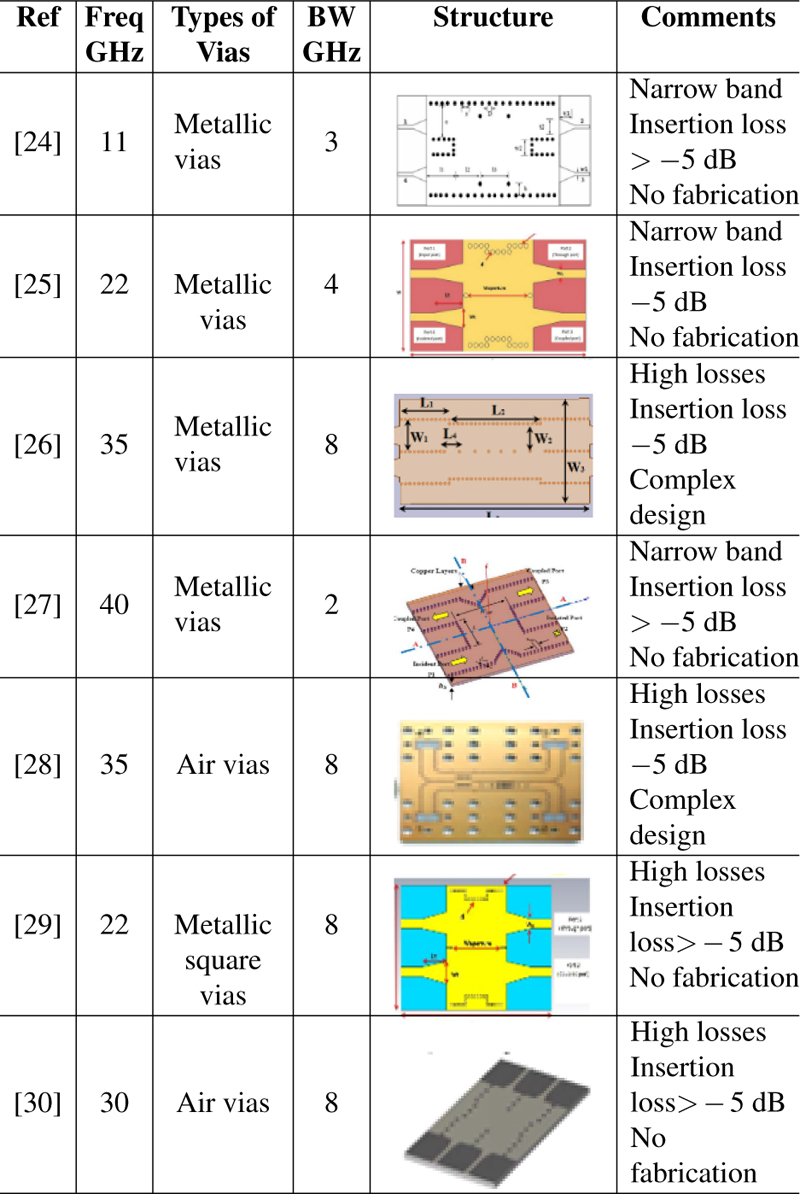
SIW is a planar waveguide technology, depicted in Fig. 1. In SIW, the wave propagates through a substrate between two rows of vias [39–41]. These vias effectively replace the metal walls found in conventional hollow waveguides. Consequently, SIW exhibits similar dispersion characteristics to those of standard waveguides [42].
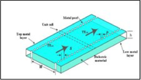
Figure 1: Substrate integrated waveguide structure [43].
SIW at millimeter-wave frequencies faces similar challenges as microstrip lines, including radiation losses, via hole issues, and dielectric losses due to the material properties [44, 45]. However, by carefully selecting suitable via diameters and spacing, these issues can be mitigated. SIW is a planar structure characterized by two rows of vias, effectively representing the narrow walls of the waveguide. Over the past few years, SIW has gained popularity among researchers as a novel transmission line technology [46]. It combines features from both microstrip and dielectric-filled waveguides (DFW) [47]. When designing SIW components, parameters such as via spacing should be carefully considered. The width between vias can be determined using the following expression [48]:
| (1) |
where a is the waveguide width from edge to edge between the two rows of vias, d is the diameter of the vias, and S is the spacing between vias. The diameter of the vias and the spacing can be calculated using:
| (2) | ||
| (3) | ||
| (4) |
where a is the width of the rectangular waveguide standard, is the substrate permittivity, and is the guided wavelength of SIW, which can be obtained using:
| (5) |
where f is the desired frequency and c is the speed of light. After discussing the equations related to SIW technology, the next section will review SIW antennas.
IV. DESIGN OF BEAMFORMING COMPONENTS
A. Design hybrid coupler
A 3-dB branch line coupler (BLC) generates output signals with a 90 phase difference. The network structure consists of four quarter-wavelength transmission lines, forming a loop. It divides input signals into two equal-amplitude signals that are 90 out of phase. The BLC can be implemented using either lumped elements or a distributed approach, as depicted in Fig. 2. At port P1, the input power is equally divided between output ports P2 and P3. Port P2 serves as the through port, P3 as the coupled port, and P4 as the isolation port, where reflections due to mismatches are directed to prevent power from reflecting back to P1. When all ports are matched, the input power delivered to the input port is evenly split between the output ports, maintaining the 90 phase difference.
Figure 2: Geometry of a conventional branch line coupler [49].
For the optimum performance of the coupler, the impedances of the shunt arms are and that of the series arms is , where is the characteristic impedance of the input and output ports, and is usually .
The return loss in a BLC quantifies the amount of power reflected from the input. Typically, it is related to S11 in decibels (dB), and the desired return loss for a BLC is typically less than 10 dB. Mathematically, the return loss can be expressed as follows [50]:
| (6) |
Insertion loss is characterized by the portion of input power at port 1 that is transmitted to the through port at port 2. It is directly related to S21 in dB. For a BLC from P1 to P2, the desired insertion loss typically falls within the range of 3 to 4 dB. Mathematically, insertion loss can be expressed as [50]:
| (7) |
The coupling factor typically represents the proportion of input power that is transferred to the output power. In this context, P1 denotes the input power at port 1, and P3 corresponds to the power output at port 3. The coupling factor is also associated with S31 in dB. For BLC, the desired coupling factor typically falls within the range 3 to 4 dB. Mathematically, the coupling factor can be expressed as [50]:
| (8) |
In a balanced line coupler (BLC), isolation refers to the difference in signal levels between isolated port 4 and input port 1. This isolation is represented by S41 in the BLC’s S-parameter. The required isolation for a BLC should be less than 10 dB. Isolation loss can be calculated using:
| (9) |
The S-matrix of a symmetrical coupler is [51]:
| (10) |
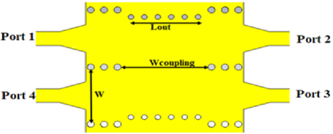
Figure 3: Structure of the proposed SIW coupler.
Figure 3 illustrates the proposed 3 dB coupler based on vias separation. To prevent signal leakage and guide the signal effectively, the coupler’s outputs are coupled using metallic vias with cuts in both the metal and substrate, resulting in an electrical length equivalent to a quarter wavelength (/4) [26]. The SIW directional coupler design features two perpendicular rectangular waveguides with a cross-region where two symmetrically placed metal posts control the signal. Additionally, two via posts at each port serve as reflection-canceling elements, achieved by varying sections of the SIW. The four ports are defined as follows: port 1 (input), port 2 (through), port 3 (coupled), and port 4 (isolated). A step impedance transition is employed between the microstrip line and SIWs to ensure a physical match of electrical and magnetic field distributions between the two media. The substrate material used is Rogers 5880 with a thickness of 0.508 mm, relative permittivity (r) of 2.2, and loss tangent of 0.0009.
Analyzing Fig. 4 (a), it becomes evident that as the width of the SIW vias decreases, the resonance frequency converges toward the desired 26 GHz frequency. Additionally, the coupling width plays a crucial role in controlling the output power at ports 2 and 3. The coupling width is determined using equation (11) [51], where 1 and 2 represent the propagation constants of the TE10 and TE20 modes, respectively. To achieve the desired operational frequency, the phase shift () must satisfy /2. This configuration tends to produce an equal power coupling ratio of 3 dB, as observed in Fig. 4 (b). Based on these findings, the vias width is set to 6.5 mm, and the coupling area is established at 11.5 mm:
| (11) |
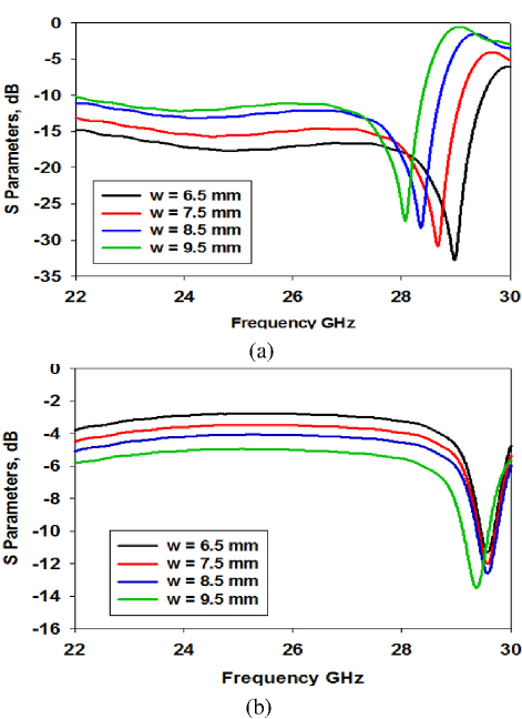
Figure 4: Simulated response (a) S11 and (b) output ports.
B. Design crossover
Crossovers are typically designed by cascading two 3-dB couplers [52]. The configuration of a 0-dB crossover is depicted in Fig. 5 (a). Our proposed crossover comprises two serially connected SIW couplers. Figure 5 (b) illustrates the crossover’s performance in terms of return loss and output power. When port 1 is excited, the return loss at 26 GHz remains below 10 dB, and the output at port 3 is 0 dB. Both port 2 and port 4 exhibit isolation values less than 10 dB at the desired frequency.
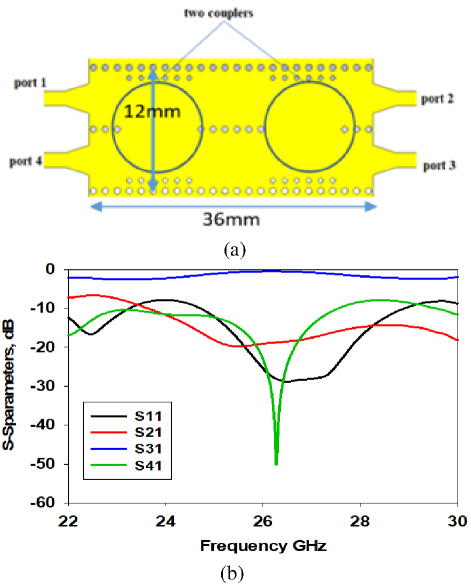
Figure 5: The proposed (a) crossover structure and (b) S-parameters.
The widths of the Schiffman phase shifters, denoted as Wt, remain consistent with the widths of the feeding transmission lines. However, the lengths of the Schiffman phase shifters, represented by Ls, vary in relation to the desired phase values. These phase shifters are implemented by extending the corresponding lengths, which are then bent into arcs. The phase difference of the phase shifters can be calculated using equation (12) [53]:
| (12) |
where Lm, Lr, and are the main length, reference length, and guide wavelength [54]. The main length, Lm, and reference length, Lr, are optimized to obtain the desired phase difference between the main line and the reference line which is at the first left output port of the proposed Butler matrix. The designed phase shifters are combined with the couplers to analyze the performance results of the Butler matrix.
C. Design phase shifter
The S-parameter response and phase shift of the proposed Schiffman phase shifter are of interest. This phase shifter employs a cylindrical metal post inserted into the SIW structure, effectively forming a T-network. The equivalent circuit, as shown in Fig. 6, accounts for the capacitive coupling between the metal sides of the SIW and the cylindrical post using two capacitors. Additionally, mutual coupling between the top and bottom metal conductors is represented by an inductance. Once all components, including the coupler, crossover, and phase shifter, are designed, they contribute to the overall performance of the Butler matrix.
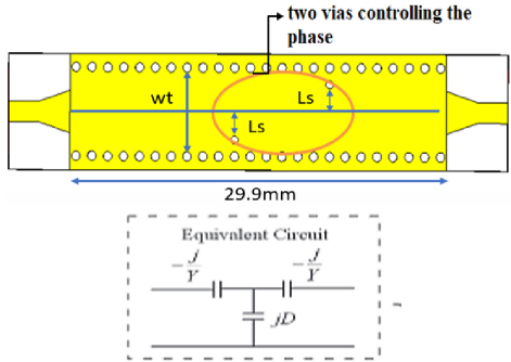
Figure 6: SIW phase shifter with two vias controllers.
V. SIW COUPLER WITH SEPARATION FEEDLINES
In this study, the SIW coupler is presented as a simulation structure (Fig. 3), with a microstrip straight feedline directly integrated into the SIW coupler. However, a significant challenge arises at higher frequencies: the limited distance between adjacent ports makes it challenging to solder SMA connectors directly to the feedline. To address this, the proposed coupler design in Fig. 3 aims to increase the spacing between adjacent ports, allowing for proper SMA soldering.
A. Simulation results of SIW coupler
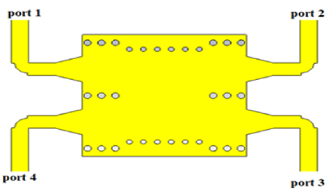
Figure 7: Final structure of the proposed coupler design.
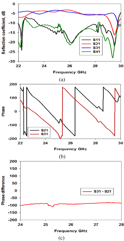
Figure 8: Simulated results of the proposed coupler with separation feedlines at port 1: (a) S-parameters, (b) phase of outputs ports, and (c) phase difference.
The feedline configuration of the proposed coupler in Fig. 3 has been adjusted. Initially, the feedlines for ports 1 and 4 were parallel, resulting in insufficient spacing between these two ports. Similarly, ports 2 and 3 faced a similar issue. To address this, the modified design in Fig. 3 now separates each pair of adjacent ports adequately. Finally, the orientation of port 1 and port 2 aligned to the top, as did that of port 3 and port 4 aligned to the bottom, allowing for the convenient soldering of SMA connectors to each port. In order to perform the measurement process, a microstrip to SIW transition line was added at each port with quarter wavelength separation for the coupler as shown in Fig. 7. The proposed coupler was re-simulated to check the effects of the separation of the feedlines on the port’s performance.
In Fig. 8, we present the simulated performance of the proposed coupler when port 1 is excited. At 26 GHz, the reflection coefficient is 20.05 dB, and the isolation is 22.12 dB, with a wider bandwidth of 5 GHz (Fig. 8 (a)). Achieving an equal power split, port 2 and port 3 exhibit 3.5 dB and 3.9 dB, respectively (Fig. 8 (a)). However, the insertion loss increases by 0.5 dB due to the additional feedlines at the output ports. The phase shift at the outputs is 91.5 (Fig. 8 (b)), and the phase difference between S31 and S21 is evident in Fig. 8 (c). Notably, the inclusion of these separation feedlines introduces a phase error of 1.5.
VI. SIW CROSSOVER WITH SEPARATION FEEDLINE
In Fig. 5 (a), the crossover integrates a microstrip feedline directly within the SIW structure, addressing a concern raised in the problem statement. However, when operating at higher frequencies, a significant challenge emerges: the proximity between neighboring ports is insufficient for attaching an SMA port directly to the feedline. Considering that the entire size of an SMA connector at 26 GHz is 14 mm, the proposed solution in Fig. 5 (a) involves increasing the spacing between adjacent ports.
A. Simulation results of SIW crossover
In the original design of the crossover shown in Fig. 5 (a), the feedlines for ports 1 and 4 were directly integrated into the SIW structure, resulting in insufficient spacing between them. A similar issue existed for ports 2 and 3. To address this, the feedline layout of the proposed crossover was modified by introducing separation between each pair of adjacent ports. As a result, the orientation of port 1 and port 2 aligns, as does the orientation of port 3 and port 4. This modification allows for successful soldering of SMA connectors to each port. To facilitate the measurement process, a microstrip-to-SIW transition line has been added at each port, with a quarter-wavelength separation for the crossover, as depicted in Fig. 9.
In Fig. 10, we observe the simulated performance of the modified feedline in the proposed crossover when port 1 is excited. At 26 GHz, the reflection coefficient is less than 28 dB, and the isolation is 16 dB (Fig. 10 (a)). Comparatively, the original crossover design in Fig. 5 (a) achieved a reflection coefficient and isolation both below 30 dB at the same frequency. Furthermore, the output power at port 3 is 1 dB (Fig. 10 (a)), whereas the original crossover’s output power in Fig. 5 (a) was very close to 0 dB. The addition of feedlines at the output ports results in a 1 dB increase in output power at port 3. Additionally, the phase at port 3 is 1 (Fig. 10 (b)), whereas the phase difference in the original crossover (Fig. 5 (a))was 0.5.
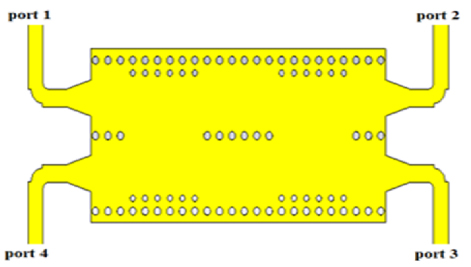
Figure 9: Final structure of the crossover design.
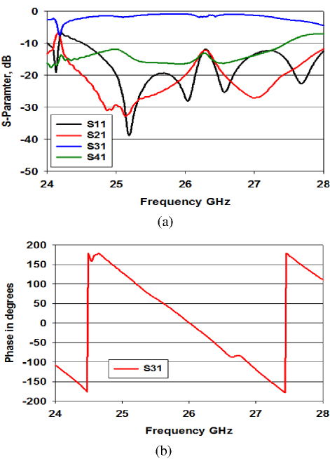
Figure 10: Simulated crossover with separation feedlines at port 1: (a) S-parameters and (b) phase outputs.
VII. FABRICATION AND MEASUREMENT OF SIW COUPLER
After completing the design phase using CST software, all components were fabricated. As indicated in Fig. 3, the fabrication process utilized a Rogers 5880 board with a thickness of 0.5 mm and a dielectric constant (r) of 2.2. JAC Engineering, Malaysia, carried out the fabrication process for the couplers. Figure 11 displays the fabricated coupler. To measure the S-parameters, two cables and two terminator loads were employed, assisted by a standard Keysight (Agilent Technologies) FieldFox N9925A vector network analyzer (VNA).
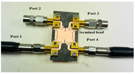
Figure 11: Fabrication of SIW coupler.
Figure 12 presents both the measured and simulated performance of the SIW coupler. At 26 GHz, the reflection coefficient was 18 dB and the isolation was 19 dB. In the simulation, the reflection coefficient and isolation were 20 and 22 dB, at the same frequency, with a wider bandwidth of 5 GHz (Fig. 12 (a)). The measured results achieved an equal power split at ports 2 and 3, with 3.9 and 4.02 dB, respectively (Fig. 12 (b)). However, due to the addition of feedlines at the output ports, there was a 1 dB increase in insertion loss. The phase difference when exciting port 1 was 91.5 in the simulation and 88 in the measurement (Fig. 12 (c)). Notably, the inclusion of these separation feedlines introduced a phase error of 2. Table 2 provides a comparison between the simulated and measured results of thecoupler.
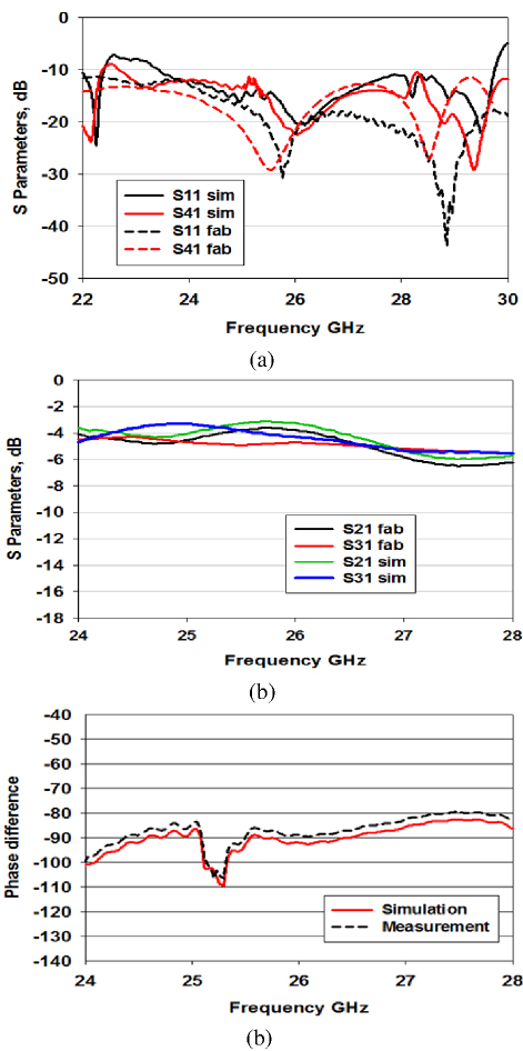
Figure 12: Measured and simulated coupler at port 1: (a) reflection coefficient and isolation, (b) S-parameters at outputs, and (c) phase difference of the outputs.
Table 2: Comparison of the coupler based on simulated and measured parameters
| Parameters | Simulated | Measured |
| Frequency GHz | 26 | 26 |
| Return loss (S) | 20.05 dB | 18 dB |
| Isolation (S) | 22 dB | 19 dB |
| Direct (S) | 3.5 dB | 3.9 dB |
| Coupling (S) | 3.9 dB | 4.02 dB |
| BW (GHz) | 5 | 5 |
| Phase diff. (degree) | 91.5 | 88 |
VIII. FABRICATION AND MEASUREMENT OF SIW CROSSOVER
Figure 13 displays the fabricated crossover, along with the measured and simulated results. In Fig. 14 (a), we observe the measured performance and simulated results of crossover in terms of its S-parameters (S11, S21, S41). At 26 GHz, the reflection coefficient is 25 dB and the isolation is 13 dB (Fig. 14 (a)). Comparatively, the simulation result shows a reflection coefficient of 1 dB. Additionally, an output power of 2 dB is achieved at port 3 (Fig. 14 (b)), whereas the simulation result is closer to 1 dB. The observed increase in output power (port 3) by 1 dB is attributed to fabrication errors and port mismatches at the output ports. Furthermore, the measured phase at port 3 is -93, with a phase error of 3 (Fig. 14 (c)). For further comparison, Table 3 presents the results for the crossover with microstrip separation feedline.
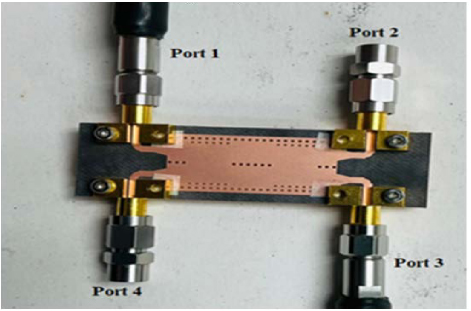
Figure 13: The fabricated crossover.
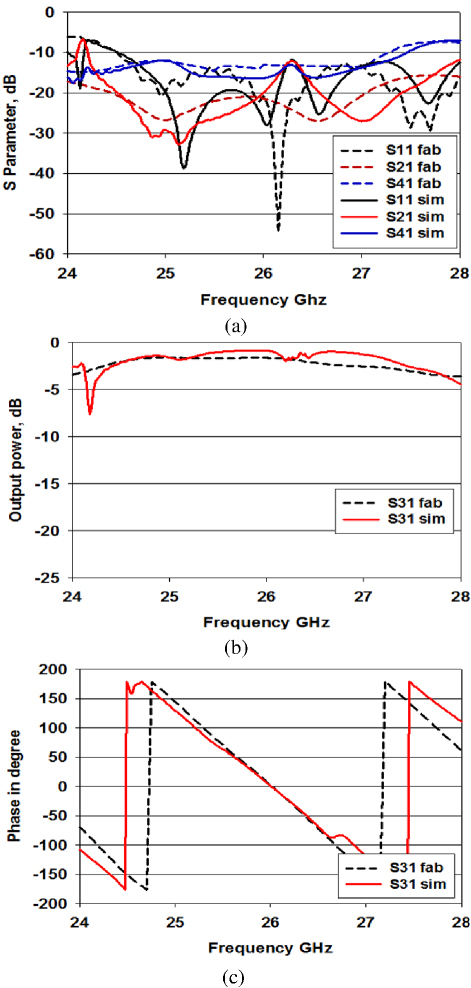
Figure 14: Measured performance of the fabricated crossover: (a) S-parameters, (b) output power at port 3, and (c) phase outputs.
Table 3: Comparison between simulated and measured results of the crossover
| Parameters | Simulated | Measured |
| Frequency GHz | 26 | 26 |
| Reflection coefficient (S) | 30 dB | 28 dB |
| Isolation (S) | 16 dB | 13 dB |
| Direct (S) | 24 dB | 22 dB |
| Coupling (S) | 1 dB | 2 dB |
| BW (GHz) | 3 | 3 |
| Phase diff. (degree) | -1 | -2 |
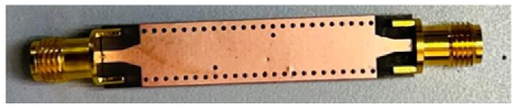
Figure 15: Printed SIW phase shifter.
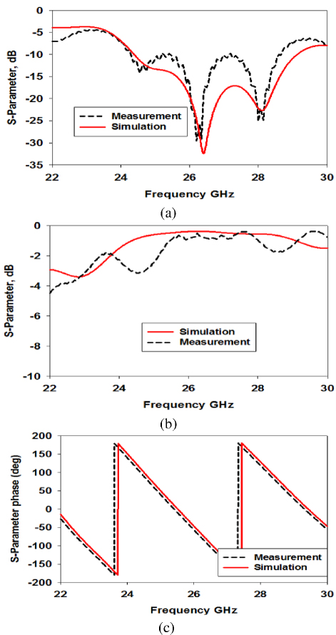
Figure 16: Measured performance of the proposed phase shifter: (a) return loss, (b) insertion loss, and (c) phase at output.
IX. SIMULATION AND MEASUREMENT RESULTS OF THE PHASE SHIFTER
In Fig. 15 we observe the printed phase shifter. The measured performance is compared to simulated results. Specifically, the reflection coefficient is below 10 dB, as depicted in Fig. 16 (a). The measured reflection coefficient at 26 GHz is 30.05 dB, slightly higher than simulated value of 32.5 dB. Moving to port 2, output power is 1.5 dB (Fig. 16 (b)), whereas the simulated output power is 0.87 dB. Consequently, additional power is accepted from the phase shifter outputs. Finally, the phase is 48 (Fig. 16 (c)), with an error of 3 compared to the simulated value of 45.
Table 4: Comparison with previously published works
| Ref. | BW (GHz) | Insertion Loss | Phase Error | Coupling |
| [18] | 2.5 | 4 dB | 4.9 | 6.57 dB |
| [20] | 2 | 4.5 dB | 8 | 5 dB |
| [19] | 3 | 2 dB | 9 | 6 dB |
| [23] | 5 | 5.3 dB | 5 | 15 dB |
| This work | 5 | 3.9, 4.02 dB | 2 | 2 dB, 3 dB |
In Table 4, we present a comparison between the simulated and measured results for the fabricated coupler, alongside previously published works. Notably, the proposed components prioritize low loss and offer an ultra-wideband performance, aligning well with the key requirements for 5G beamforming networks at millimeter-wave frequencies
X. CONCLUSION
A SIW coupler and crossover with low loss profile in magnitude and phase are proposed in this paper at 26 GHz. Coupler and crossover are designed by distributing vias along the SIW structure while carefully controlling the spacing between them. The designed coupler and crossover are simulated using CST software and fabricated using Rogers 5880. The measured and simulated results showed an impedance bandwidth of more than 5 GHz with a minimum return loss of 19 dB at 26 GHz. A 3-dB coupling ratio obtained at output ports with a perfectly 88 phase difference. Overall, the proposed coupler and crossover are suitable to use in the design of a full beamforming networks at Ka-band.
ACKNOWLEDGMENT
This work was supported by the Ministry of Higher Education (MOHE) under Fundamental Research Grant Scheme FRGS/1/2021/STG04/UTM/01/1 and grant 09G19 School of Postgraduate Studies (SPS), Research Management Centre, Advanced RF and Microwave Research Group, Faculty of Electrical Engineering, Universiti Teknologi Malaysia (UTM), Johor Bahru.
REFERENCES
[1] L. Sun, S. G. Zhou, and G. X. Zhang, “Synthesis method of an orthogonal beamforming network with arbitrary ports for shaped beams,” IEEE Trans. Antennas Propag., vol. 70, no. 6, pp. 4794-4802, 2022.
[2] J. W. Lian, Y. L. Ban, H. Zhu, and Y. J. Guo, “Uniplanar beam-forming network employing eight-port hybrid couplers and crossovers for 2-d multibeam array antennas,” IEEE Trans. Microw. Theory Tech., vol. 68, no. 11, pp. 4706-4718, 2020.
[3] K. Ding and A. A. Kishk, “Extension of Butler matrix number of beams based on reconfigurable couplers,” IEEE Trans. Antennas Propag., vol. 67, no. 6, pp. 3789-3796, June 2019.
[4] H. Ren, H. Zhang, Y. Jin, Y. Gu, and B. Arigong, “A novel 2-D 3 X 3 Nolen matrix for 2-D beamforming applications,” IEEE Trans. Microw. Theory Tech., vol. 67, no. 11, pp. 4622-4631.
[5] M. Farahani, M. Akbari, M. Nedil, T. A. Denidni, and A. R. Sebak, “A novel low-loss millimeter-wave 3-dB 90 ridge-gap coupler using large aperture progressive phase compensation,” IEEE Access, vol. 5, pp. 9610-9618, 2017.
[6] H. Zhu, M. Ansari, and Y. J. Guo, “Wideband beam-forming networks utilizing planar hybrid couplers and phase shifters,” IEEE Trans. Antennas Propag., vol. 70, no. 9, pp. 7592-7602, 2022.
[7] J. Lai, T. Yang, P. L. Chi, and R. Xu, “2-2.2 GHz reconfigurable 1 4 filtering beamforming network using novel filtering switch-coupler and twisted rat-race coupler,” IEEE Trans. Microw. Theory Tech., vol. 70, no. 4, pp. 2462-2472,2022.
[8] M. Kishihara, K. Yamane, and I. Ohta, “Design of cruciform directional couplers in E-plane rectangular waveguide,” IEEE MTT-S Int. Microw. Symp. Dig., no. 2, pp. 1722-1725, 2006.
[9] M. M. Pezhman and A. A. Heidari, “Design of compact SIW-based multi-aperture coupler for Ku-band applications,” in ICEE 2019 - 27th Iran. Conf. Electr. Eng., pp. 1338-1341, 2019.
[10] J. W. Lian, X. Y. Zhao, Y. L. Ban, Y. Liu, and Z. Nie, “Compact SIW 2-D Butler matrix and its multibeam application,” IEEE Antennas Wirel. Propag. Lett., vol. 20, no. 3, pp. 386-390, 2021.
[11] Q. L. Yang, Y. L. Ban, J. W. Lian, Z. F. Yu, and B. Wu, “SIW Butler matrix with modified hybrid coupler for slot antenna array,” IEEE Access, vol. 4, pp. 9561-9569, 2016.
[12] S. Y. Zheng and X. F. Ye, “Ultra-compact wideband millimeter-wave crossover using slotted SIW structure,” in 2016 IEEE International Workshop on Electromagnetics: Applications and Student Innovation Competition (iWEM), IEEE, pp. 1-2, May 2016.
[13] E. B. Abubakirov, Y. M. Guznov, S. V. Kuzikov, A. S. Shevchenko, A. A. Vikharev, and S. A. Zapevalov, “Quasi-optical input mode coupler for a Ka-band multimegawatt gyroklystron,” IEEE Trans. Microw. Theory Tech., vol. 66, no. 3, pp. 1273-1278, 2018.
[14] B. Sutbas, E. Ozbay, and A. Atalar, “Accurate isolation networks in quadrature couplers and power dividers,” IEEE Trans. Circuits Syst. II Express Briefs, vol. 68, no. 4, pp. 1148-1152, 2021.
[15] Z. Zhao and T. A. Denidni, “Millimeter-wave printed-RGW hybrid coupler,” IEEE Microw. Wirel. Components Lett., vol. 30, no. 2, pp. 156-159, 2020.
[16] Y. M. Hussein, M. K. A. Rahim, N. A. Murad, and H. O. Hanoosh, “Low loss wideband 44 Butler matrix networks based on substrate integrated waveguide for 5G applications,” IEEE Access, vol. 12, pp. 7896-7910, 2024.
[17] J. W. Lian, Y. L. Ban, J. Q. Zhu, K. Kang, and Z. Nie, “Compact 2-D scanning multibeam array utilizing the SIW three-way couplers at 28 GHz,” IEEE Antennas Wirel. Propag. Lett., vol. 17, no. 10, pp. 1915-1919, 2018.
[18] M. Boulesbaa, T. Djerafi, A. Bouchekhlal, and B. Mekimah, “Design of a directional coupler based on SIW technology for X band applications,” in CCSSP 2020 - 1st Int. Conf. Commun. Control Syst. Signal Process., pp. 85-89, 2020.
[19] T. Qiao, J. Zhang, and Q. S. Cheng, “Space-mapping based automatic design of SIW-based directional coupler with arbitrary power ratio,” IEEE J. Multiscale Multiphysics Comput. Tech., vol. 7, pp. 200-206, 2022.
[20] N. Sun, Y.-J. Zhao, X.-y. Yang, and H.-w Deng, “A simple SIW balanced directional coupler with high common-mode suppression,” Microwave and Optical Technology Letters, vol. 65, no. 2. pp. 434-440, 2023.
[21] M. Bučo and S. T. Imeci, “Design and fabrication of a 6dB compact directional coupler,” Sustain. Eng. Innov., vol. 3, no. 2, pp. 68-72, 2021.
[22] S. T. Imeci and K. Temur, “Center-slotted wideband hybrid 10 dB coupler,” J. Eng. Res., vol. 11, no. 1, pp. 285-296, 2023.
[23] X. Shi and X. Zhu, “Design of SIW parallel coupling coupler at q-band,” in 2017 IEEE 6th Asia-Pacific Conf. Antennas Propagation, APCAP 2017 - Proceeding, pp. 1-3, 2018.
[24] A. Nasri, H. Zairi, and A. Gharsallah, “Design of a novel structure SIW 90 coupler,” Am. J. Appl. Sci., vol. 13, no. 3, pp. 276-280, 2016.
[25] N. Khalid, S. Z. Ibrahim, F. H. Wee, and F. S. Mahmud, “Substrate integrated waveguide (SIW) 3 dB coupler for K-Band applications,” EPJ Web Conf., vol. 162, 2017.
[26] M. J. Tavakoli and A. R. Mallahzadeh, “Wideband directional coupler for millimeter wave application based on substrate integrated waveguide,” Emerg. Sci. J., vol. 2, no. 2, pp. 93-99, 2018.
[27] W. M. Abdel-Wahab and S. Safavi-Naeini, “Low loss H-shape SIW hybrid coupler for millimeter-wave phased arrays antenna systems,” IEEE Antennas Propag. Soc. AP-S Int. Symp., pp. 5-6, 2012.
[28] T. Li and W. Dou, “Substrate integrated waveguide 3 dB directional coupler based on air-filled vias,” Electron. Lett., vol. 53, no. 9, pp. 611-613, 2017.
[29] N. Khalid, S. Z. Ibrahim, and W. F. Hoon, “K-band substrate integrated waveguide (SIW) coupler,” IOP Conf. Ser. Mater. Sci. Eng., vol. 341, no. 1, 2018.
[30] Z. Kordiboroujeni, J. Bornemann, and T. Sieverding, “Mode-matching design of substrate-integrated waveguide couplers,” in 2012 Asia-Pacific Symp. Electromagn. Compat. APEMC 2012 - Proc., pp. 701-704, 2012.
[31] G. E. Ponchak and E. Tentzeris, “Development of finite ground coplanar (FGC) waveguide 90 degree crossover junctions with low coupling,” IEEE MTT-S Int. Microw. Symp. Dig., vol. 3, pp. 1891-1894, 2000.
[32] J. Yao, C. Lee, and S. P. Yeo, “Microstrip branch-line couplers for crossover application,” IEEE Trans. Microw. Theory Tech., vol. 59, no. 1, pp. 87-92, 2011.
[33] T. Djerafi and K. Wu, “60 GHz substrate integrated waveguide crossover structure,” in 2009 European Microwave Conference (EuMC), Rome, Italy, pp. 1014-1017, 2022.
[34] A. B. Guntupalli, T. Djerafi, and K. Wu, “Ultra-compact millimeter-wave substrate integrated waveguide crossover structure utilizing simultaneous electric and magnetic coupling,” in IEEE MTT-S Int. Microw. Symp. Dig., pp. 31-33, 2012.
[35] W. J. Liu, S. Y. Zheng, Y. M. Pan, Y. X. Li, and Y. L. Long, “A wideband tunable reflection-type phase shifter with wide relative phase shift,” IEEE Trans. Circuits Syst. II Express Briefs, vol. 64, no. 12, pp. 1442-1446, 2017.
[36] D. N. A. Zaidel, S. K. A. Rahim, R. Dewan, S. F. Ausordin, and B. M. Saad, “Square-shaped phase shifter using multilayer technology for ultra wideband application,” in RFM 2013 - 2013 IEEE Int. RF Microw. Conf. Proc., pp. 22-25, 2013.
[37] S. Y. Zheng, W. S. Chan, and K. F. Man, “Broadband phase shifter using loaded transmission line,” IEEE Microw. Wirel. Components Lett., vol. 20, no. 9, pp. 498-500, 2018.
[38] K. Y. Kapusuz and U. Oguz, “Millimeter wave phased array antenna for modern wireless communication systems,” in 2016 10th Eur. Conf. Antennas Propagation, EuCAP 2016, no. 1, pp. 1-4,2016.
[39] M. W. Almeshehe, N. A. Murad, M. K. A. Rahim, O. Ayop, F. Zubir, M. Z. A. Aziz, M. N. Osman, and H. A. Majid, “Low loss waveguide-based Butler matrix with iris coupling control method for millimeterwave applications,” Waves in Random and Complex Media, vol. 33, no. 2, pp. 372-392,2023.
[40] Y. M. Hussein, M. K. A. Rahim, N. A. Murad, H. O. Hanoosh, and N. B. Muhamad Nadzir, “Substrate integrated waveguide antenna at millimeter wave for 5G application,” Appl. Comput. Electromagn. Soc. J., vol. 37, no. 4, pp. 478-484, 2022.
[41] R. Lovato and X. Gong, “A third-order SIW-integrated filter/antenna using two resonant cavities,” IEEE Antennas Wirel. Propag. Lett., vol. 17, no. 3, pp. 505-508, 2018.
[42] H. Jin, G. Q. Luo, W. Wang, W. Che, and K. S. Chin, “Integration design of millimeter-wave filtering patch antenna array with SIW four-way anti-phase filtering power divider,” IEEE Access, vol. 7, pp. 49804-49812, 2019.
[43] Q. Tan, Y. Guo, L. Zhang, F. Lu, H. Dong, and J. Xiong, “Substrate integrated waveguide(SIW)-based wireless temperature sensor for harsh environments,” Sensors (Switzerland), vol. 18, no. 5, pp. 1-13, 2018.
[44] S. Ji, Y. Dong, and Y. Fan, “Low-profile dual-band filtering antenna with a shared SIW cavity,” IEEE Antennas Wirel. Propag. Lett., vol. 20, no. 10, pp. 2053-2057, 2021.
[45] C. Fan, B. Wu, Y. L. Wang, H. Y. Xie, and T. Su, “High-gain SIW filtering antenna with low H-plane cross polarization and controllable radiation nulls,” IEEE Trans. Antennas Propag., vol. 69, no. 4, pp. 2336-2340, 2021.
[46] https://www.microwaves101.com/encyclopedias/substrate-integrated-waveguide
[47] M. Bozzi, F. Xu, D. Deslandes, and K. Wu, “Modeling and design considerations for substrate integrated waveguide circuits and components,” in 8th Int. Conf. Telecommun. Mod. Satell. Cable Broadcast. Serv. TELSIKS 2007, Proc. Pap., 2007.
[48] S. Moitra, A. Kumar Mukhopadhyay, A. K. Bhattacharjee, and A. Kumar Bhattacharjee, “Ku-band substrate integrated waveguide (SIW) slot array antenna for next generation networks,” Glob. J., vol. 13, no. 5, 2013.
[49] S. Gomha, E. S. M. El-Rabaie, A. A. T. Shalaby, and A. S. Elkorany, “Design of new compact branch-line coupler using coupled line dual composite right/left-handed unit cells,” Optoelectron. Adv. Mater. Rapid Commun., vol. 9, no. 5-6, pp. 836-841, 2015.
[50] M. Boulesbaa, T. Djerafi, A. Bouchekhlal, and B. Mekimah, “Design of a directional coupler based on SIW technology for X band applications,” in 2020 1st International Conference on Communications, Control Systems and Signal Processing (CCSSP), El Oued, Algeria, pp. 85-89, 2020.
[51] K. B. Kumar and T. Shanmuganantham, “SIW hydride coupler for mm-wave applications,” in 2016 Int. Conf. Control Instrum. Commun. Comput. Technol. ICCICCT 2016, pp. 246-250, 2017.
[52] Y. Y. Cao, Y. W. Wu, Z. Jiang, and Z. C. Hao, “A compact millimeter-wave planar directional coupled crossover with a wide bandwidth,” IEEE Microw. Wirel. Components Lett., vol. 30, no. 7, pp. 661-664, 2020.
[53] B. W. Xu, S. Y. Zheng, Y. M. Pan, and Y. H. Huang, “A universal reference line-based differential phase shifter structure with simple design formulas,” IEEE Trans. Components, Packag. Manuf. Technol., vol. 7, no. 1, pp. 123-130, 2017.
[54] H. Peng, P. Jiang, T. Yang, and H. Jin, “Continuously tunable SIW phase shifter based on the buried varactors,” IEICE Electron. Express, vol. 12, no. 7, 2015.
BIOGRAPHIES

Yaqdhan Mahmood Hussein was born in Samawah, Iraq, in 1991. He received the B.S. in computer techniques engineering in 2014-2015 from Islamic University College in Najaf City, and M.S. degrees in electronic engineering (telecommunication system) from Universiti Teknikal Malaysia Melaka (UTeM), Malaysia, in 2018. He currently studies the Ph.D. degree in electronic engineering in Universiti Teknologi Malaysia (UTM) in Johor Bahru city. His current research interests include millimeter-wave antennas, base station antennas, and SIW technology with Butler matrix.

Noor Asniza Murad (Senior Member, IEEE) received the first degree in electrical engineering majoring in telecommunication and the master’s degree in engineering from the Universiti Teknologi Malaysia (UTM), in 2001 and 2003, respectively, and the Ph.D. degree in 2011 for research on micromachined millimeter-wave circuits under supervision of Professor Lancaster. She joined the Department of Radio Communication Engineering (RaCED), Faculty of Electrical Engineering (FKE), UTM, as a Tutor. She was appointed as a Lecturer in April 2003. She joined the Emerging Device Technology Group, University of Birmingham, UK. She was with HID GLOBAL Sdn Bhd for one year under Research and Development specifically working on RFID tag design, testing and development. She is leading the Advance RF and Microwave Research Group, School of Electrical Engineering, UTM. Her research interests include antenna design for RF and microwave communication systems, millimeter-wave circuits design, RFID, and antenna beamforming. She is a member of Antenna and Propagation (AP/MTT/EMC) Malaysia Chapter.

Mohamad Kamal A. Rahim (Senior Member, IEEE) was born in Alor Setar, Kedah, Malaysia, in 1964. He received the B.Eng. degree in electrical and electronic engineering from the University of Strathclyde, UK, in 1987, the master’s degree in engineering from the University of New South Wales, Australia, in 1992, and the Ph.D. degree in the field of wideband active antenna from the University of Birmingham, UK, in 2003. From 1992 to 1999, he was a Lecturer with the Faculty of Electrical
Engineering, Universiti Teknologi Malaysia, where he was a Senior Lecturer with the Department of Communication Engineering, from 2005 to 2007. He is currently a Professor with the Universiti Teknologi Malaysia. His research interests include the design of active and passive antennas, dielectric resonator antennas, microstrip antennas, reflect array antennas, electromagnetic bandgap, artificial magnetic conductors, left-handed metamaterials, and computer-aided design for antennas.

Hatem Oday Hanoosh was born in Samawah, Iraq, in 1991. He received the B.S in computer techniques engineering in 2014 from Islamic University College in Najaf city, the master’s degree in electronic engineering (telecommunication system) from Universiti Teknikal Malaysia Melaka (UTeM), Malaysia, in 2018, and the Ph.D. degree in the field of waveguide Nolen matrix from the Universiti Teknologi Malaysia (UTM) in Johor Bahru city in 2023. He is currently a Professor with the AL-Muthanna University of Engineering Electronics and Communication Department. His research interests include the design of antennas, dielectric resonator antennas, waveguide antennas, reflect array antennas, Nolen matrix, and designs for slot antennas.
ACES JOURNAL, Vol. 39, No. 11, 999–1011
doi: 10.13052/2024.ACES.J.391108
© 2024 River Publishers