Nanoarray of Vivaldi Rectenna for Infrared-energy Harvesting
Wided Amara, Abdelaziz Alzahrani, Ameni Mersani, Donia Oueslati, Ahmed Elsharabasy, Bandar Hakim, Hatem Rmili, and Atef Elsherbeni
1Electrical and Computer Engineering Department, Faculty of Engineering, King Abdulaziz University
P.O. Box 80204, Jeddah 21589, Saudi Arabia
hmrmili@kau.edu.sa
2K. A. CARE Energy Research and Innovation Center
King Abdulaziz University, Jeddah 21589, Saudi Arabia
3ESPRIT School of Business
ZI. Chotrana II, Tunis P.O. Box 160, Tunisia
4Electrical and Computer Engineering Department
McMaster University, Hamilton, ON L8S 4K1, Canada
5Electrical Engineering Department
Colorado School of Mines, Golden, Colorado 80401, USA
aelsherb@mines.edu
Submitted On: July 8, 2020; Accepted On: September 11, 2023
ABSTRACT
This article presents the design of an array of rectennas operating at 28.3 THz for infrared (IR) energy harvesting applications. The basic element of the array consists of a Vivaldi-dipole rectenna composed of two arms made with different conductors (gold and titanium). A metal-insulator-metal (MIM) tunnel diode is used to rectify the THz ac current. The proposed MIM diode consists of a very thin layer of AlO sandwiched between the two metal electrodes. Arrays of two, three, and four rectennas are investigated. The improvement of the energy captured by coupling several elements in the same structure with a common gap is also investigated. This array architecture, without feeding network, may reduce the number of rectifying diodes and, therefore, decrease losses and increase the overall efficiency. Finally, it has been found that the four-elements rectenna array has a maximum electric field intensity of 62.4 10 V/m at 28.3 THz.
Index Terms: Energy harvesting, infrared (IR) energy, MIM diode, rectenna, THz, Vivaldi antenna array.
I. INTRODUCTION
Nowadays, wireless sensor networks are widely used in several applications related to industry, surveillance, monitoring of people and objects, home automation, scientific research, etc. This rapid expansion in using wireless systems is due, among other reasons, to the considerable developments and advances made in microelectronics. These advances have enabled the integration of more and more functionalities in an increasingly smaller volume [1].
Unfortunately, research and development in energy storage technologies have not followed the same rapid trend. As a result, portable communications systems are finding themselves increasingly penalized regarding autonomy. To make these communication systems and objects more self-sufficient in energy and to increase the battery life, efficient electromagnetic energy harvesting systems are required. Collecting energy from the surrounding environment and converting it into usable electrical energy is a very interesting alternative to traditional usage of replaceable batteries [2]. These energy sources can be recovered from artificial devices or available natural sources [3–4].
The most direct and abundant source of energy comes from the Sun. Photovoltaic energy harvesting is a promising technology that converts solar energy in the visible spectrum into usable electrical energy [5], but this received energy from the sun is used in the visible region during the day only.
The energy released at night is in the infrared (IR) region within the spectral range 7-17 μm with a maximum power peak centred around the wavelength 10.6 μm (28.3 THz) [6–7]. In order to harvest and convert this available infrared energy, we need new devices to capture, convert, and store this energy. One solution that can exploit this abundant infrared energy from the Earth’s surface is to use energy harvesting based on nano-rectennas [4, 8]. A rectenna-based system, is composed of a receiving antenna with integrated rectifying diode [9–11].
Harvesting energy in the IR domain requires efficient design of the antenna and the rectifying diode, with deep understanding of the dielectric properties of materials in the optical band, especially in the infrared range [4, 12, 13].
The continuous technological evolution of electronic and optical materials at the nano-metric scale quickly leads to the design of devices which were not even possible a few years ago. Plasmonics is one of areas that benefit most from these advances [14–15]. Optical antennas are strongly analogous to their radio frequency counterparts, but there are crucial differences in their physical properties and behavior when scaled. Most of these differences arise because metals are not perfect conductors at optical frequencies, but rather are highly correlated plasmas described as a free electron gas. By definition, an optical antenna is a device that converts freely the radiation of propagating light into localized electromagnetic energy, and vice versa [16]. The fabrication of optical antenna structures is an emerging opportunity for new optoelectronic devices [17]. Optical antennas help to exceed the diffraction limit, making it possible to manipulate, control and visualize optical fields at the nano-metric scale, which offers a wide range of applications [18]. Among these are antenna probes for nano-imaging, non-linear signal conversion, and IR energy harvesting. These nano-antennas require specific studies to develop optical antennas.
Associated with the antenna, IR energy harvesting is based on the use of diodes as rectifiers. In the terahertz domain, the use of diodes and more particularly of Schottky and MIM diodes, is very useful at the level of the rectifier block. MIM diodes are very attractive and promising candidates for energy recovery in the infrared spectrum. The MIM diodes are a good candidate for infrared (IR) applications of the electromagnetic spectrum because of their high-speed characteristics and their compatibility with integrated circuits [4, 19].
Usually, a single rectenna element cannot supply sufficient captured wireless power. To increase the power recovered by the system, we must maximize the power captured. One way to achieve this is by increasing the surface area of the antennas; however, this will shift the omni-directional bandwidth toward the low frequencies. Another approach is to combine several elements in an array configuration. Several configurations of the second approach are already presented in literature, but they all suffer from some limitations: In [20], a rectenna array based on a 2-by-4 misaligned bowtie antenna is presented. Four spiral elements composed of three gold-based square spiral nano-antennas resonate near 13 μm [21] with dimensions of 750 750 nm of each element. The system arrays have been coupled together in one structure with one common gap by using a feeding line. In both configurations cited in [20] and [21], the size of the feeding network is large compared to the array causing high ohmic losses, which reduce the intensity of the total collected electric field within the gap.
To increase further the captured electric field in arrays of nano-rectennas, authors in [22] optimized both the metal thickness of a bowtie nano array, (the optimal thickness was equal to 95 nm) in addition to the incident angle.
In this paper, we present a new design of nano-rectenna array, based on a Vivaldi rectenna operating at infrared wavelengths, with a maximum peak of collected power situated at 10.6 μm (28.3 THz). The structure is composed of an array of Vivaldi nano-rectennas placed in a configuration to create a hot spot in order to increase the intensity of the collected electric field within this localized zone. The main advantage of the proposed configuration is to remove the complex and lossy feeding network used in [22] and [23], in addition to the concentration of the electric field in one small region (hot spot) where the rectifying diode should be integrated. So, losses will be reduced, the captured electric field within the gap will be enhanced, and the total efficiency of the rectenna will be increased.
This article is organized as follows. Section II describes, respectively, the designs of one, two, three, and four antennas and their performances. The maximum fields captured for each case are presented. In section III, a similar study adds the rectifying MIM diode to form the rectennas. The design parameters of the Vivaldi nanoarrays are optimized to obtain maximum performance. The rectennas were simulated by using computer simulation technology (CST) software [24], where the dielectric properties of the metals (gold and titanium) are calculated based on the Drude-model.
II. VIVALDI NANO-ANTENNA
A. Vivaldi nano-antenna design
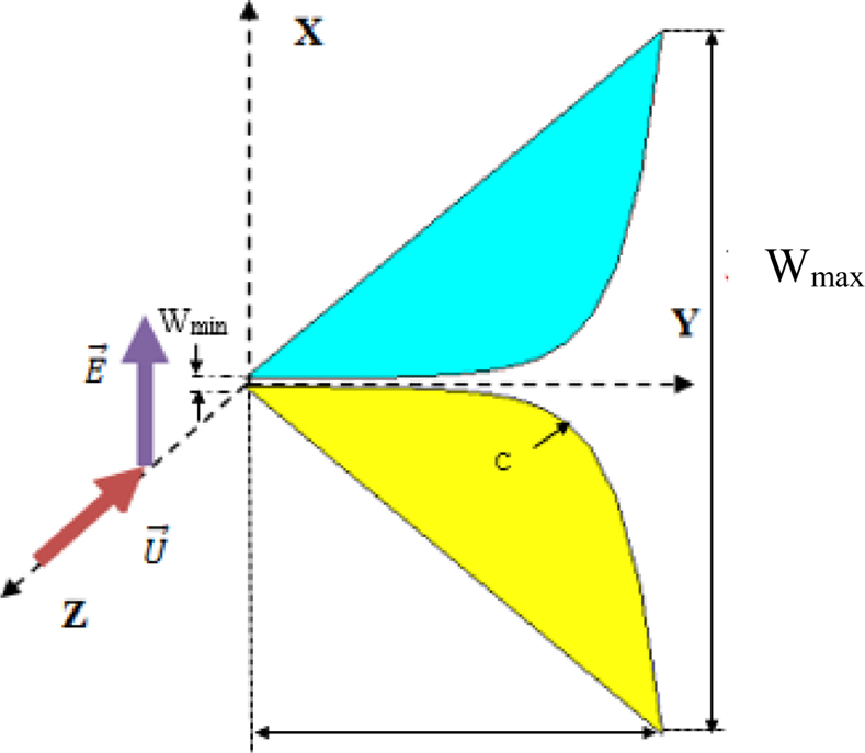
Currently, printed antennas are becoming more and more important because of the great variety of geometric shapes they can take, which make them applicable to different integration situations. This is a key property which explains the introduction of printed antennas in energy harvesting applications. This technology responds well to the needs of our application. Therefore, the design of the antennas must respond to compromises in terms of performance and complexity of implementation. The Vivaldi antenna is a simple planar antenna characterized by a wide band and linear polarization. The antenna element as shown in Fig. 2, presents an exponential curve profile in the XY plane. In The gap between the two arms of the antenna is defined by the following function [25]:
| (1) |
where the coefficient C is the curvature parameter, W is the width of the gap line, and R is defined by:
| (2) |
W is the opening width at the end of the arm and C is the length of the arm. The antenna configuration is symmetric around the x-axis.
The antenna element is composed of two arms: one in gold, with a dielectric constant , loss tangent tan , and a thickness h; and the other in titanium with a dielectric constant , loss tangent tan , and a thickness h separated by a gap W. A detailed parametric study allowed us to obtain the optimal values of the different parameters of the final structure Vivaldi antennas are described in Table 1.
The dielectric properties of gold, used in the simulations are obtained by presenting the experimental data in a Drude model [4]:
| (3) |
where represents the contribution of electrons linked to the relative dielectric constant, is the frequency of the plasma (rapid oscillation of the electron density in conductive media such as metals), and is the amortization frequency.
Table 1: Antenna dimensions and material properties
| Parameters | Value (μm) | Parameters | Value(μm) |
|---|---|---|---|
| Wmax | 40 | at 28.3 THz | 6037.7 |
| Wmin | 0.05 | tan at 28.3 THz | 0.4 |
| L | 2.7 | at 28.3 THz | 430 |
| h | 0.08 | tan at 28.3 THz | 0.98 |
| hg | 0.08 | C | 1.8 |
The advantage of this configuration is that it gives the designer the freedom to vary several antenna parameters in order to increase the electric field received. In addition, it produces a stronger electric field in its gap. Another advantage of Vivaldi’s nano-antennas of this form is the ability to build an array by coupling many elements of the Vivaldi antenna in one configuration and combining the electric field of each element at the feed point of the network, where a rectifier can be integrated.
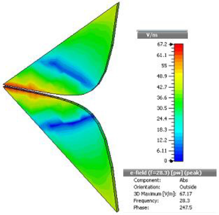
Light is an electromagnetic wave where the electric and magnetic fields are perpendicular to the direction of propagation (z-axis). To study the electric field at the antenna gap, a linear polarized plane wave (along x-axis) with an electric field module equal to 1 V/m (see Fig. 2). The electric field component of the incident field is along the dipole axis y, and the direction of propagation is perpendicular to the dipole (along -z). The maximum value of the collected field is concentrated at the gap with a value 67.2 V/m at 28.3 THz, as shown in Fig. 2.
Figure 1: Configuration parameters of the Vivaldi nano-antenna and direction of incident plane wave.
Figure 2: Field distribution at 28.3 THz.
B. Vivaldi nano-antenna array
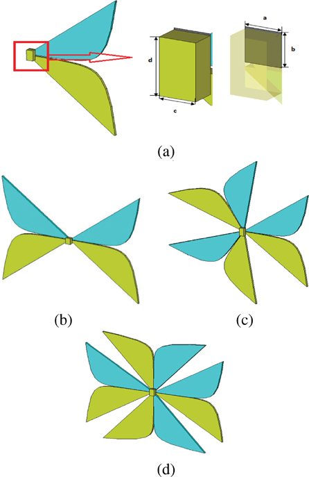
Vivaldi nano-antenna arrays have been used and studied due to their suitability for broadband operation and because they offer flexibility to optimize radiation properties by adjusting their configuration [22]. Figure 3 shows the configuration of the studied nano arrays. We started by designing a nanoarray of two elements to increase the captured electric field [26]. This network consists of two nano-antennas with a 30 nm gap to collect the electric field from the elements of the array, as shown in Fig. 3 (a). This simple design offers a higher electric field compared to a single element nano-antenna.
The dimensions of all nano-antennas in this array are the same as those in Fig. 2 with a slot of 30 nm separating the two identical nano-antennas. Figure 3 (b) shows three Vivaldi nano-antenna arrays based on gold and titanium, coupled together in a single network common gap. The nano-antenna arrays have been designed to resonate around 28.3 THz. Then, the four-element planar Vivaldi nanoarray, shown in Fig. 3 (c), has been designed to increase the electric field picked up for IR energy harvesting applications [22]. By coupling numerous elements in the geometry of an array, the far-field characteristics are improved and the output voltage is increased. In previous studies [8], methods of increasing the captured electric field by modifying the geometric parameters of the nano-antenna are presented. From the simulated results, the maximum electric field is produced by a 7 nm gap between the arms of the antenna. In addition, the captured electric field is improved if the size of the gap between the elements of the network at the supply point is reduced. Therefore, for the array of four elements, a Vivaldi nanoarray based on the optimized parameters is constructed to obtain maximum performance.
Figure 3: Vivaldi nano-antenna: (a) single structure, (b) two elements array, (c) three elements array, and (d) four elements array.
C. Discussion
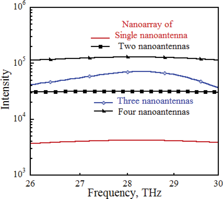
Figure 4 compares the solar energy harvesting capacities of the different arrays.
The intensity of single nano-antenna reaches a maximum value of 5 10 at 28.3 THz. The captured field is not sufficient with such a single-element antenna. However, this nano-antenna offers the possibility of capturing higher values by using it in a circular or hexagonal network by capturing the fields at the center of the array. In the case of a simple antenna, the received signal is often not sufficient to drive the rectifier. Thus, it is necessary to increase the gain of the receiving antenna by increasing its electrical size. This can be accomplished by assembling the single element antennas in a circular array configuration. The total field captured by the array is determined by the addition of the fields captured by each individual element when the elements interfere constructively. The factors which control the overall performances of an array with identical elements are presented in [26]: the geometrical configuration, the space between the elements, the amplitude and the phase of excitation of the elements, and the contribution of the individual element. As we can see in Fig. 4, it is obvious that the four-antenna nanoarray reaches a maximum value of 10 at 28.3 THz, which is better for harvesting the electric field compared to other designs. It can be seen that the field captured at the center increases by increasing the number of nano-antennas integrated into the array.
This significant improvement in the collected field strength obtained with the nanoarray is mainly due to the increase in numbers of dipoles used. and therefore the increase in its electrical size, at the resonant frequency.
Figure 4: The intensity variation captured vs. frequency for the different Vivaldi nanoarrays.
III. VIVALDI RECTENNA NANOARRAY
Electromagnetic energy harvesting systems require a wave receiving antenna connected to an RF/DC conversion system, thus forming a rectifier device or “Rectenna.” Currently, many challenges encountered in the design of rectennas for high performance are being studied. It leads to continuous progress in the understanding of light/matter interaction at optical frequencies. Recently, some researchers have shown a new low-cost nano-antenna manufacturing method [22].
Due to the geometric convenience of the dipole, the Vivaldi nano-antenna is chosen in this work to be the main resonator that integrates with the rectifier. However, the electric field picked up at the center of its gap is weak and needs to be further improved. That’s why an auxiliary resonant element is added to the structure, at the center of this nano-antenna, in order to increase the captured field and improve its overall performance.
Regarding diodes, many promising new alternatives are being explored. For example, metal-insulator-metal (MIM) diodes, metal insulator-insulator-metal diodes (MIIM), traveling wave diodes, pointy diodes, and geometric diodes have been considered as potential candidates for these applications.
In this work, firstly, the dipole nano-antenna is simulated. The field picked up at the feed gap level is shown in Fig. 4. After that, the optimized nano-antenna is exploited in the rectenna structure by inserting a MIM diode. In fact, a rectangular dielectric layer of AlO with a permittivity equal to at 28.3 THz, thickness 1.5 nm, and size 0.21 μm is placed above the center of the simulated nano-antenna. A rectangular gold conductive layer of length d = 0.35 μm, width c = 0.2 μm, and thickness 0.14 μm is inserted as shown in Fig. 5 (a).
Then, the designed double nano-antenna, composed of four Vivaldi arms forming an array of two dipoles, is used to create a nano-rectenna array. These two elements have been coupled in the form of an array by adding a single diode, as shown in Fig. 5 (b).
A. Nano-rectenna array design
The MIM diode is used for IR rectification with the optical nano-antenna. The diode incorporates an insulator layer between two electrodes, which are sufficiently thin to allow tunnel conduction. To integrate the MIM diode into the nanoarray of two Vivaldi antennas, we followed the same principle of the MIM rectifier, an insulator layer of dimension 0.2 0.105 μm and of the same thickness, then a conductive layer of gold of dimension 0.2 0.25 μm is inserted in the same area of thediode.
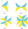
Figure 5: Nano-rectenna configuration: (a) single array, (b) two elements, (c) three elements, and (d) four elements.
The Vivaldi planar nanoarray (2 3) designed to increase the electric field picked up for solar energy collection applications is shown in Fig. 5 (c). The far-field characteristics are improved by coupling numerous elements in the form of an array, and the output voltage is increased. The dimensions of the MIM diode are each time modified in order to reach a maximum value of the field at the frequency of the resonance. A single diode was used for the network of three elements. The insulating layer of AlO of dimension 0.2 0.215 μm was used in the simulation. We have selected the conductive layer of gold of dimension 0.2 0.355 μm in our study. Four Vivaldi elements, coupled together in a single array with a common gap, is shown in Fig. 5 (d). All of the features in Fig. 5 (d) have the same dimensions as the Vivaldi nano-antenna, as depicted in Fig. 2. A single diode was used for the array of threeelements.
Figure 6: The intensity variation vs. frequency for different studied nanoarrays.
IV. DISCUSSION
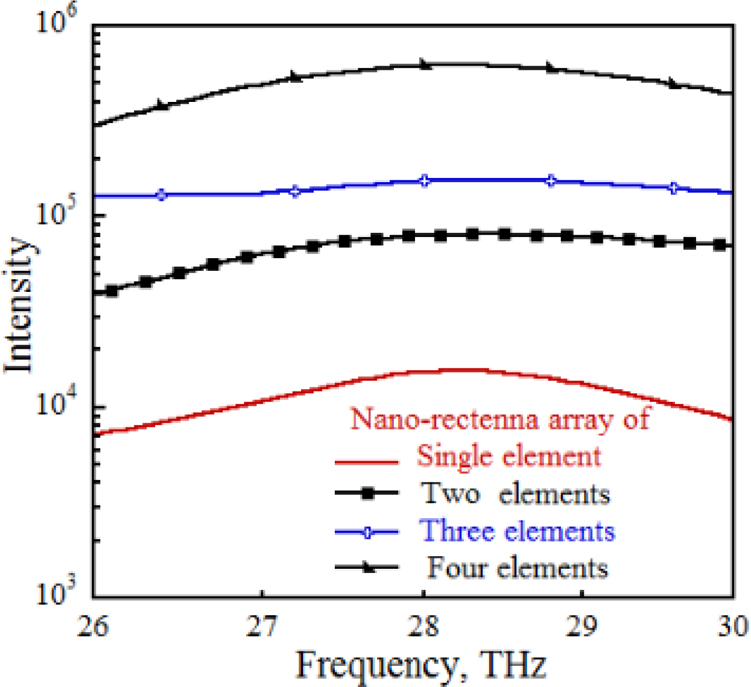
The electric fields captured inside the common gap of the one, two, three, and four-element nanoarray are calculated and plotted versus frequency from 26 THz to 30 THz, as shown in Fig. 6.
The Vivaldi nano-antenna array resonates at 13 μm. Furthermore, it is clear that the Vivaldi network with four elements at the highest captured electric field, which is more than six times greater than that of the array with a single element. The intensity of the electric field increases by increasing the number of elements forming the nanoarray.
Thus, in this approach, the arrays designed have contributed to increasing the field of view at the level of the common gap when a single rectifier is necessary instead of two or more. This means that we have reduced the heat losses in the rectifiers and increased the total efficiency of the rectenna.
Table 2 summarizes the simulation results of the Vivaldi nano-rectennas designed. Vivaldi nano-rectennas resonate at 28.3 THz, and they always operate in the desired infrared band. Furthermore, it is clear that the Vivaldi array with four elements produces the highest captured electric field, which is more than double the highest value for the two-element array, and more than four times the highest value for the single Vivaldi element.
Table 2: Comparison between different Vivaldi nano-rectenna configurations
| Array Element | E-max (V/m) | Intensity |
|---|---|---|
| One element | 124 | 1.5 10 |
| Two elements | 284 | 8 10 |
| Three elements | 393 | 15.4 10 |
| Four elements | 790 | 62.4 10 |
V. CONCLUSION
A Vivaldi nano-antenna array for solar energy harvesting application at infrared frequencies 26-30 THz is designed and optimized. The first study is done to examine the captured field at the common gap for the single, double, three, and four nano-antenna with a resonant frequency of 28.3 THz. The second study is done by integrating a MIM diode into the designed arrays. The MIM diode is a very thin device made up of a very thin layer of AlO sandwiched between two metal electrodes. It is noted that the resonant frequency for this array is 28.3 THz with a maximum electric field intensity of value 62.4 10 J for a nanoarray of four elements.
ACKNOWLEDGMENT
The Deanship of Scientific Research at King Abdulaziz University, Jeddah, Saudi Arabia has funded this project, under grant no. KEP-MSc: 41-135-1443. The authors also acknowledge the support provided by King Abdullah City for Atomic and Renewable Energy (K.A.CARE) under the K.A.CARE-King Abdulaziz University Collaboration Program.
REFERENCES
[1] X. W. Yao, D. B. Ma, and C. Han, “ECP: A probing-based error control strategy for THz-based nanonetworks with energy harvesting,” IEEE Access, vol. 7, pp. 25616-25626, 2019.
[2] A. Takacs, H. Aubert, S. Fredon, L. Despoisse, and H. Blondeaux, “Microwave power harvesting for satellite health monitoring,” IEEE Trans. on Microwave Theory Tech, vol. 62, no. 4, pp. 1090-1098, April 2014.
[3] F. Yildiz, “Potential ambient energy-harvesting sources and techniques,” J. Technol. Studies, vol. 35, no. 1, pp. 40-48, 2009.
[4] W. T. Sethi, “Optical antennas for harvesting solar radiation energy,” Ph.D. Thesis, Rennes University, 2019.
[5] R. Singh, G. F. Alapatt, and A. Lakhtakia, “Making solar cells a reality in every home: Opportunities and challenges for photovoltaic device design,” IEEE Journal of the Electron Devices Society, 2013.
[6] A. Yahyaoui, A. Elsharabasy, J. Yousaf, K. Sedraoui, and H. Rmili, “MIIM-based optical log spiral rectenna for efficient IR energy harvesting,” Alexandria Engineering Journal, vol. 61, no. 11, pp. 8897-8909, 2022.
[7] W. Amara, D. Oueslati, N. Eltresy, A. Alghamdi, K. Sedraoui, T. Aguili, H. Rmili, and R. Mittra, “Parametric study of modified dipole nano-antennas printed on thick substrates for infrared energy harvesting,” Int. J. Numer. Model., e2704. https://doi.org/10.1002/jnm.2704, 2019.
[8] D. K. Kotter, W. D. Slafer, S. D. Novack, and P. Pinhero, “Solar antenna electromagnetic collectors,” ASME, Jacksonville, Florida, USA, 2008.
[9] M. Gadalla, M.-R. Abdelrahman, and A. Shamim, “Design, optimization and fabrication of a 28.3 THz nano-rectenna for infrared detection and rectification,” Scientific Reports, 4:4270, DOI: 10.1038/srep04270, Mar. 2014.
[10] W. Haboubi, H. Takhedmit, J.-D. L. S. Luk, S.-E. Adami, B. Allard, F. Costa, C. Vollaire, O. Picon, and L. Cirio, “An efficient dual-circularly polarized rectenna for RF energy harvesting in the 2.45 GHz ISM band. Progress in Electromagnetics Research, vol. 148, pp. 31-39, ff10.2528/ PIER14031103ff, 2014.
[11] C. A. Reynaud, D. Duché, J.-J. Simon, E. Sanchez-Adaime, O. Margeat, J. Ackermann, V. Jangid, C. Lebouin, D. Brunel, F. Dumur, D. Gigmes, G. Berginc, C. A. Nijhuis, and L. Escoubas, “Rectifying antennas for energy harvesting from the micro-waves to visible light: A review,” Progress in Quantum Electronics, Elsevier, vol. 72, p. 100265, 2020.
[12] O. P. Dimitriev, “Harvesting of the infrared energy: Direct collection, up-conversion, and storage,” Optoelectronics and Optoelectronic Devices, SPQEO, vol. 22, no. 4, pp. 457-469, 2019.
[13] J. Shank, E. A. Kadlec, D. W. Peters, and P. S. Davids, “Infrared nanoantenna-coupled rectenna for energy harvesting,” IEEE Aerospace Conference, Big Sky, MT, USA, pp. 2-9, March 2019.
[14] P. Biagioni, J. S. Huang, and B. Hecht, “Nano-antennas for visible and infrared radiation,” Rep. Prog. Phys., vol. 75, no. 024402, 2012.
[15] C. De Angelis, A. Locatelli, D. Modotto, S. Boscolo, M. Midrio, F. Sacchetto, A. D. Capobianco, F. M. Pigozzo, and C. G. Someda, “Extending antenna theory to the optical domain,” 2009 European Microwave Conference (EuMC), 2009.
[16] G. A. E. Vandenbosch, Plasmonics - Principles and Applications, intechOpen, 2012.
[17] M. Mivelle, “Etude et developpement de nano-antennes brees pour la microscopie en champ proche optique et la nano-photonique,” Ph.D. Thesis, September-October 2009.
[18] J. Paparone, “Contrôle de l’émission dans des nano-structures plasmoniques: Nanoantennesmultimères et plasmons long-range,” Optique/photonique, Ph.D. Thesis, Université Lyon 1 – Claude Bernard, 2016.
[19] E. G. Arsoy, M. Inac, A. Shafique, M. Ozcan, and Y. Gurbuz, “The metal-insulator-metal diodes for infrared energy harvesting and detection appli-cations,” Proc. SPIE 9819, Infrared Technology and Applications XLII, May 20, 2016.
[20] M. Aldrigo, D. Masotti, V. Rizzoli, and A. Costanzo, “Design rules for innovative nano-rectennas in the infrared region,” 2013 European Microwave Conference, Nuremberg, pp. 1-4, 2013.
[21] A. Sabaawi, C. Tsimenidis, and B. Sharif, Rectenna Solar Cells. 10.1007/978-1-4614-3716-1_11, 2013.
[22] A. M. A. Sabaawi, C. C. Tsimenidis, and B. S. Sharif, “Planar bowtie nanoarray for Thz energy detection,” IEEE Transactions on Terahertz Science and Technology, vol. 3, no. 5, pp. 1-8, 2013.
[23] A. M. A. Sabaawi, C. Tsimenidis, and B. Sharif, “Bow-tie nano-array rectenna: Design and optimi-zation,” Antennas and Propagation (EUCAP), 2012 6th European Conference on IEEE, pp. 1975-1978, 2012.
[24] CST Microwave Studio, ver. 2012, Computer Simulation Technology, Framingham, MA, 2012.
[25] C. A. Balanis, Antenna Theory: Analysis and Design, 2005.
[26] A. W. A. Sabaawi, C. C. Tsimenidis, and B. S. Sharif, “Infra-red nano-antennas for solar energy collection,” Loughborough Antennas and Propa-gation Conference (LAPC), pp. 1-4, 2011.
BIOGRAPHIES

Wided Amara has received her B.S. in industrial electronics engineering in October 2015, and the M.S. in smart systems for communication in November 2016, from the National Engineering School of Sousse (ENISO, Tunisia). She received her Ph.D. in tele-communications within the SysCom laboratory, ENIT, Tunis, Tunisia, in 2021. Her field of interest is infrared energy harvesting.

Abdulaziz Alzahrani was born in Abha, Saudi Arabia, May 1988. He received the MSc. degree in iElectronic / communication engineering with the Department of Electrical Engineering, King Abdul- Aziz University, Jeddah, Saudi Arabia, in 2023. His research interests include energy harvesting, renewable energy, nano-technology, and green power generation.

Ameni Mersani received a degree in electronics, computer and information science from the University Tunis El Manar, Tunisia, in 2009 and the master thesis in electronics from the Faculty of Science of Tunis, Tunisia, in 2012. She received a Ph.D. in engineering sciences (electronics) from the University of Tunis El Manar, 2018. From September 2018, she has been working as a research assistant in ISET’COM (Department of Telecommunication). From December 2019, she has been a post-doctoral researcher with King Abdulaziz University, Saudi Arabia. Her research mainly focuses on the development of the design of wearable antennas for wireless applications and metamaterials, dipole antennas, and infrared energy harvesting.

Donia Oueslati received a degree in electronics, computer and information science from the University Tunis El Manar, Tunisia, in 2008 and the Master thesis in system of communications from National Engineering School of Tunis, Tunisia, in 2011. She received the Ph.D. in engineering sciences from Université Catholique de Louvain, Belgium, and in telecommunication from UTM in 2017. From April 2017 to August 2018, she was a post-doctoral researcher with Antenna Lab, Université Catholique de Louvain, in collaboration with HEC research center, EMC Lab, University of Central Florida, Orlando, Florida, USA, and ECE Department, King Abdulaziz University, Saudi Arabia. Since September 2018, she has been working as research assistant at University Catholique de Louvain. Her research mainly focuses on the development of a modal analysis methods for printed structures based on the Method of Moments and singular decomposition to identify a chipless radio frequency identification (RFID) and to localize a reader. Her research interests include ultra-wideband (UWB) optical rectennas for solar energy harvesting, investigation of irregular fractal antennas, and low-profile antenna array and array optimization for 5G applications.

Ahmed Y. Elsharabasy received a B.Sc. degree in electronics and communications engineering from Cairo University, Egypt, in 2004 with distinction (honors). He joined the Department of Engineering Mathematics and Applied Physics, Cairo University as a teaching and research assistant. In 2012, he received a Master’s degree in engineering mathematics from Cairo University. His master focused on yield optimization of EM-based structures. In this research he carried out statistical optimization using space-mapping surrogates, and utilized HFSS to simulate the microwave circuit performance. In 2014, he joined the Electrical and Computer Engineering Department at McMaster University, Canada, as a Ph.D. researcher on IR and THz energy harvesting. His research focused on design, modeling, optimization, fabrication, and characterization of rectenna devices for ambient (waste) thermal energy harvesting and detection applications. He also introduced novel designs of optical antennas and perfect metamaterial absorbers. Additionally, he succeeded in tuning the performance of metal-mesh THz filters via topology optimization to fit with specific applications. He received the McMaster International Excellence Award in 2016, 2017, and 2018. In 2020, Ahmed joined the University of Toronto, Canada, as a postdoctoral research fellow to develop low-power, large-area optical phased array for free-space optical communication in satellite and space applications.
Ahmed is a member of IEEE, OSA, SPIE. He is currently a visiting scholar in the Electrical and Computer Engineering Department at McMaster University, Canada. Elsharabasy is author/coauthor of 17 journal and conference papers and presentations. His research interests include nano-antennas, MIM diodes, plasmonics, photonics, energy harvesting, and optimization.

Bandar Hakim is an assistant professor of electrophysics at KAU. He received his Ph.D. degree in electrophysics from the University of Maryland. He worked with the Medical Robotics group at the École Polytechnique Fédérale de Lausanne in Switzerland, the Center for Devices and Radiological Health at the Food and Drug Administration in Washington, DC, and the Neurology department at Mount Sinai School of Medicine in New York, NY. He served as an industrial consultant in the US, Switzerland, and Germany.

Hatem Rmili received the B.S. degree in general physics from the Science Faculty of Monastir, Tunisia, in 1995, and the DEA diploma from the Science Faculty of Tunis, Tunisia, in quantum mechanics, in 1999. He received the Ph.D. degree in physics (electronics) from both the University of Tunis, Tunisia, and the University of Bordeaux 1, France, in 2004. From December 2004 to March 2005, he was a research assistant in the PIOM laboratory at the University of Bordeaux 1. From March 2005 to March 2007, he was a postdoctoral fellow at the Rennes Institute of Electronics and Telecommunications, France. From March to September 2007, he was a postdoctoral fellow at the ESEO Engineering School, Angers, France. From September 2007 to August 2012, he was an associate professor with the Mahdia Institute of Applied Science and Technology (ISSAT), Department of Electronics and Telecommunications, Tunisia. He is associate professor with the Electrical and Computer Engineering Department, Faculty of Engineering, King Abdulaziz University, Jeddah, Saudi Arabia.
Rmili’s research interests concern applied electro-magnetic applications involving antennas, metamaterials, and métasurfaces. The main targeted applications are reconfigurable antennas for multi-standard wireless communications systems, security of chipless RFID systems with fractal tags, terahertz photoconductive antennas for infrared energy harvesting, UWB nano-rectennas for collection of solar energy, phase shifters for low-cost 5G communication systems, and microwave absorbing materials for stealth technologies.

Atef Z. Elsherbeni started his engineering career as a part-time software and system design engineer from March 1980 to December 1982 at the Automated Data System Center, Cairo, Egypt. From January to August 1987, he was a post-doctoral fellow at Manitoba University. He joined the faculty at the University of Mississippi in August 1987 as an assistant professor of Electrical Engineering. He advanced to the rank of associate professor in July 1991 and the rank of professor in July 1997. He was the director of The School of Engineering CAD Lab from August 2002 to August 2013, and the director of the Center for Applied Electromagnetic Systems Research (CAESR) from July 2011 to August 2013. He was appointed Associate Dean of Engineering for Research and Graduate Programs from July 2009 to July 2013 at the University of Mississippi. Elsherbeni became the Dobelman Distinguished Chair and Professor of Electrical Engineering and Computer Science at the Colorado School of Mines in August 2013. He was appointed as adjunct professor, at the Department of Electrical Engineering and Computer Science of the L.C. Smith College of Engineering and Computer Science at Syracuse University, in January 2004. He spent a sabbatical term in 1996 at the Electrical Engineering Department, the University of California at Los Angeles (UCLA) and was a visiting professor at Magdeburg University during the summer of 2005 and at the Tampere University of Technology in Finland during the summer of 2007. In 2009, he was selected as Finland Distinguished Professor by the Academy of Finland and TEKES. Elsherbeni is a fellow member of the Institute of Electrical and Electronics Engineers (IEEE) and a fellow member of The Applied Computational Electromagnetic Society (ACES). He is the editor-in-chief for ACES Journal and a past associate editor to the Radio Science Journal.
ACES JOURNAL, Vol. 38, No. 7, 513–521
doi: 10.13052/2023.ACES.J.380707
© 2023 River Publishers
