A Low-profile Dual-band Frequency Selective Surface with High Selectivity at its Higher Passband
Jian Jiao, Nianxi Xu, and Jinsong Gao
1School of Physics
Changchun Normal University, Changchun 130032, China
xinhe7hl@126.com
2Key Laboratory of Optical System Advanced Manufacturing Technology
Changchun Institute of Optics, Fine Mechanics and Physics, Chinese Academy of Sciences
Changchun 130033, China
xnxlzhy999@126.com
3Jilin Provincial Key Laboratory of Advanced Optoelectronic Equipment and Instruments Manufacturing Technologies
Changchun 130033, China
gaojs@ciomp.ac.cn
Submitted On: February 18, 2024; Accepted On: August 27, 2024
ABSTRACT
In order to meet the requirements for multiband communication, a dual-band passband frequency selective surface (FSS) with low-profile and high selectivity at its higher passband is proposed in this paper. The proposed FSS is a three-layer structure. An arc-cross patch (ACP) and four quarter-circular patches (QCP) are introduced on the outer layers to produce two transmission nulls of the higher passband, which result in high selectivity of higher passband. The inductively complementary structure on the middle layer is introduced to manipulate the coupling between layers which contribute to the low-profile and angular stability. The segmental study method is used to establish the equivalent circuit model (ECM) and analyze its mechanism. The proposed dual-band FSS, whose high selectivity was verified by experiment, is low-profile and shows good polarization insensitivity and angular stability. A feasible FSS design solution is provided for dual-band communication.
Index Terms: Complementary structure, dual-band, frequency selective surfaces, high selectivity, low-profile.
I. INTRODUCTION
Frequency selective surfaces (FSSs) are two-dimensional periodic structures which can control the propagation of electromagnetic waves and are widely used in antenna [1], radome [2], satellite communication [3], electromagnetic shielding [4], and so on. With the development of communication technology, the demands of multi-band communication systems have increased. Therefore, the study of FSSs that meet the application requirements of multi-band communication systems is of great significance [5][6].
In previous studies, various techniques have been proposed to develop multiband performance. In [7], a dual-band 3D FSS with close band spacing were designed based on SCW structure. One modified parallel-plate waveguide propagation path and one SCW propagation path are responsible for dual passband, and the counteraction between them contributes to transmission zeros, resulting in a high selectivity of 2.65 at the higher passband. Nevertheless, its thickness is 0.145, where refers to the free-space wavelength corresponding to the center frequency of the lower passband. In [8], based on an interlaced grid arrangement, a 3D dual-band FSS with large band ratio is proposed. Grating structures form higher passbands, and the additional wire-grid polarizers form the lower passband. It has poor selectivity. Its thickness is 0.139, and its upper passband response is not stable when the incident angle increases to 40. In [9], the proposed unit cell is evolved from a cross-shaped structure surrounded by an inductive grid. Diagonal feed networks are proposed to accomplish the dc bias, and different transmission poles are produced by soldering different varactors to diagonal units. It is angular stable, and its thickness is only 0.007. However, it shows poor selectivity, and lumped elements would introduce large insertion loss. Cascaded FSSs is the most popular approach to design multi-band FSSs [10][11]. The FSS proposed in [10] is a three-layer structure. One metallic cross-shaped grid layer is sandwiched by two metallic layers with a split ring-shaped slot. The slots in the outer layer are responsible for the lower passband, and the three-layer FSS forms a second order hybrid resonator at higher bandpass. Its thickness is 0.017 and its SF value is 2.14 at higher passband. In [11], a frequency-selective rasorber is presented. The lossy layer is a combination of a loop with loaded resistors and three folded loops, and the FSS layer consists of double hexagon loop slots. Its two transmission poles are generated by two parallel LC circuits. Its thickness is 0.16 and its SF value is 2.71 at higher passband. The performance of the FSSs in the above literatures are compared with this work inTable 1.
In this paper, a novel dual-band passband FSS with low-profile and high selectivity at higher passband is presented. The lower passband has one transmission pole whereas the higher passband has two transmission poles. Its thickness is reduced to 0.015 and the performance of selectivity is improved to 1.85. The structure consists of three metallic layers and two thin dielectric substrates. An arc-cross patch (ACP) and four quarter-circular patches (QCP) are introduced in the outer layer to generate two transmission nulls which are the key factors in forming fast roll-off characteristics of the higher passband. A complementary structure of the outer layer is introduced in the middle layer to regulate the coupling between layers, which plays an important role in forming the low-profile and angular stability. The proposed FSS, which is insensitive to polarization, can be a potential candidate for multibandapplications.
Table 1: Comparison of this work with previously reported FSS
| FSS | f & f(GHz) | Angular Stability | Thickness() | SF |
| [9] 2022 | 1.43/2.09 | 60 | 0.007 | 7.5/9.72 |
| [8] 2022 | 2.5/15.5 | 40 | 0.139 | 6.0/5.0 |
| [11] 2019 | 6.1/10.1 | 30 | 0.16 | 2.86/2.71 |
| [7] 2019 | 5.46/7.15 | 45 | 0.145 | 12.6/2.65 |
| [10] 2018 | 3.2/6.7 | 45 | 0.017 | 5.71/2.14 |
| This work | 8.4/13.7 | 45 | 0.015 | 4.28/1.85 |
| is the property of roll-off, where refers to the bandwidth of -30 dB passband and refers to the bandwidth of -3 dB passband [12]. | ||||
II. DUAL-BAND FSS DESIGN AND CIRCUIT ANALYSIS
A. Design description
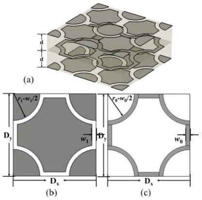
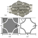
Figure 1 shows the proposed dual-band bandpass FSS structure which consists of three metallic layers separated from one another by two thin dielectric substrates. The unit cell of the top and bottom layers consists of an ACP at the center with four QCP (forming circular patches in a periodic array) present at each corner. The unit cell of the middle layer is the complementary structure of the outer layers.
The relative permittivity of the two thin substrates is 2.2 (ignoring its loss tangent in simulation) and the optimized thickness of them is d 0.35 mm. Other optimized dimensional parameters of the unit cell are given as follows: D D 10 mm, r 3.4 mm, w 1.0 mm, r 3.5 mm, and w 1.0 mm.
Figure 1: FSS geometry: (a) 3D view of a 22 array, (b) unit cell of the top and bottom layers, and (c) unit cell of the middle layer.
B. Circuit analysis and mechanism
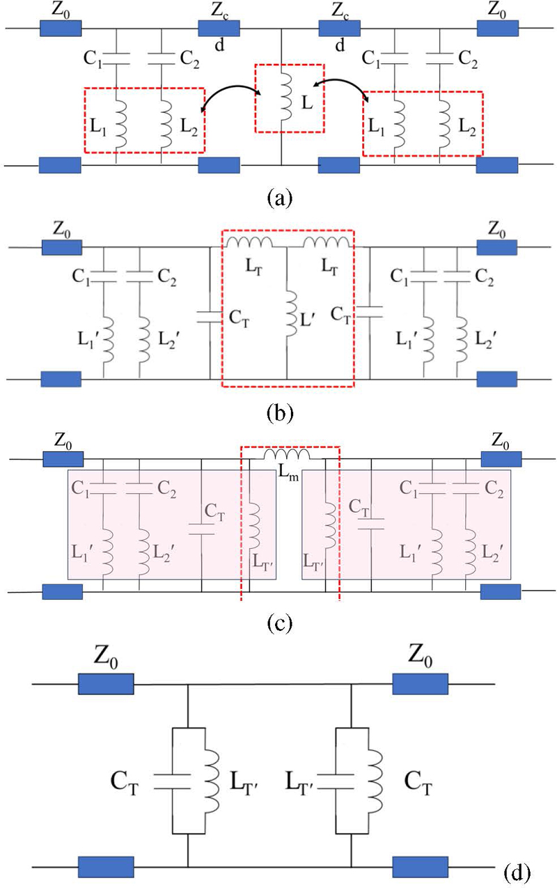
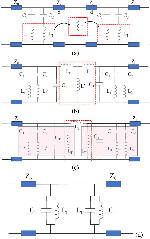
To better understand the operation of this structure, its ECM is shown in Fig. 2 (a). The ACP and QCP in the top and bottom layers can be modeled as a parallel of two series LC resonators (L-Cand L-C) [13]. The metallic wire in the middle layer acts as a shunt inductance L. The magnetic coupling between outer layers and middle layer is taken into account. The coupling changes the values of self-inductance into L, L, and L. The semi-infinite free space on both sides of the FSS is represented by intrinsic wave impedance Z 377 . The two dielectric substrate layers can be modeled as the same short piece of transmission line whose characteristic impedance is . Its equivalent circuit is a series inductor L and shunt capacitor C, which is shown in Fig. 2 (b).
Two hybrid LC resonators are coupled to one another by inductor L after converting the T-network composed of inductors Land L into a -network composed of Land L, as shown in Fig. 2 (c).
Figure 2: ECM of the proposed FSS (a) with transmission lines, (b) using series inductor L and shunt capacitor Cinstead of transmission lines, (c) after converting the T-network into a -network, and (d) equivalent circuit at its lower passband.
The segmental study method is used to analyze its mechanism. At the lower passband, the parallel L-C resonators are the dominant resonant mechanism, and the filter can be reduced to two parallel resonators, as shown in Fig. 2 (d). The equivalent impedance Z of the proposed FSS working at lower passband can be expressed as:
| (1) |
Thus, one transmission pole can be obtained when goes to infinity, which means that the FSS would transmit the EM wave at that frequency value. Based on this analysis, the transmission pole at the lower passband can be expressed as:
| (2) |
A second order coupled-resonator bandpass filter with inductive coupling shown in Fig. 2 (c) is responsible for the higher passband. The impedance of the hybrid LC resonator as shown in the shaded area in Fig. 2 (c) is:
| (3) |
Here, , , and are:
| (4) | |||||
| (5) | |||||
| (6) |
The equivalent impedance Z of the proposed FSS working at higher passband can be expressed as [14]:
| (7) |
For the hybrid LC resonator, if the series resonator L-C resonates, a transmission zero will be formed at f. Similarly, another transmission zero will be formed at fwhen the series resonator L-C resonates. The EM wave would be reflected by the proposed FSS at these two resonant frequencies which can be expressed as:
| (8) | |||||
| (9) |
Two transmission poles would be formed when Z goes to infinite [15], and expressed as:
| (10) | |||||
| (11) |
where the variables a, b, and c are expressed as:
| (12) | ||||
| (13) | ||||
| (14) |
and located outside and could regulate the fast roll-off characteristics of sidebands at higher passband.
The simplified ECMs shown in Figs. 2 (c) and (d) are good approximations for us to understand its mechanism which has been validated in the Agilent Advanced Design System (ADS) research presented in Section IIIA.
III. SIMULATION RESULTS
A. Normal incidence
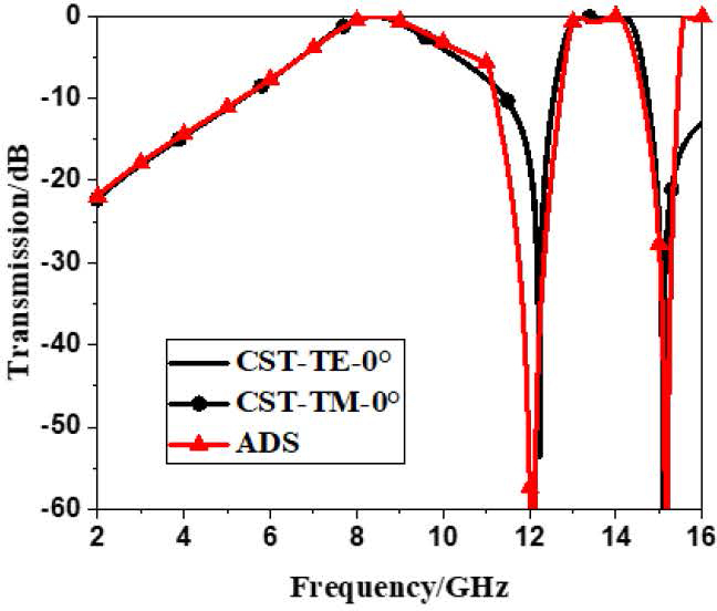
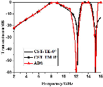
Simulations are conducted with the structure parameters provided in Section IIA by using CST Microwave Studio. Figure 3 presents the simulated S. The structure is polarization insensitive. The proposed FSS exhibits dual-band bandpass response with lower passband (S -3 dB) from 7.17 GHz to 9.71 GHz, and higher passband (S -3 dB) from 12.8 GHz to 14.5 GHz. The lower passband exhibits the first-order response, and its transmission pole exists at 8.4 GHz. Meanwhile, the higher passband exhibits second-order response with a sharp roll-off at sidebands, and its two peaks exist at 13.25 GHz and 14.1 GHz between which a valley exists at 13.7 GHz.
Figure 3: Transmission characteristics of the proposed dual-band FSS.
The segmental study method is used to analyze the ECMs of the proposed FSS by the ADS. The ECM shown in Fig. 2 (c) characterizes the higher passband of the proposed FSS from about 11 GHz to 15.5 GHz. The ECM shown in Fig. 2 (d) characterizes the lower passband of the proposed FSS before about 11 GHz. The values of L and C could influence the quality factor of the two passband simultaneously, hence the values of L and C in Figs. 2 (c) and (d) should be the same.
The optimized values of the circuit parameters in Figs. 2 (c) and (d) are L 2.276 nH, C 0.155 pF, L 9.95 nH, L 25.6 nH, C 0.0175 pF, C 0.0043 pF, and L 2.96 nH. That C is larger than theoretical value is attributed to the strong electric field located at the gap between the metallic patches. The circuit simulation result of S is also presented in Fig. 3 and a good match is found with full-wave simulation. There is some discrepancy around 11-12 GHz, because 11-12 GHz is the critical range between two ECMs. The discrepancy is a little larger after 15.5 GHz, but it is outside the working band. The discrepancy of lower transmission null between ADS and CST is 0.15 GHz, and that of higher transmission null is 0.09 GHz. These discrepancies mean that these circuit parameters need finer optimization, and our circuit models need improvements. However, the ECMs in Figs. 2 (c) and (d) are sufficient to explain the mechanism of the proposed FSS.
B. Oblique incidence
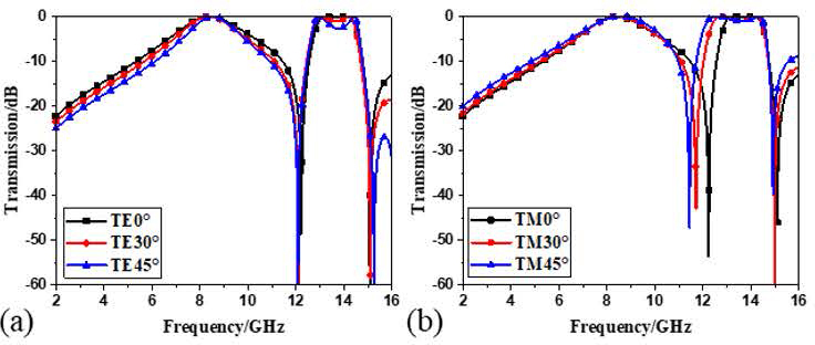
The calculated S of the proposed FSS to the angle of incidence is shown in Fig. 4. Figure 4 (a) shows the frequency response of the FSS for TE polarization. As the angle of incidence increases, the bandwidth of the two passbands does not considerably change, but the band ripple of the higher passband increases. For the TM incidence as shown in Fig. 4 (b), the bandwidth of the higher passband increases and the passband ripple decreases, as the angle of incidence increases.
Figure 4: Calculated transmission coefficients of the proposed FSS for different incidence angles: (a) TE polarization and (b) TM polarization.
The lower passband shows better angular stability with incidence angle variation than the higher passband. The frequency response of the proposed FSS is relatively stable at 45 for both TE and TM polarizations.
As the angle of incidence varies, the variations observed in the bandwidth of the structure can be attributed to the change of wave impedance, which in turn will change the loaded quality factor of the coupled resonators [16]. For TE incidence, the wave impedance changes as Z/cos. The quality factor Qof the hybrid resonators shown in Fig. 2 (c) increases for large incidence angles. The bandwidth corresponding to each transmission pole of the higher passband is reduced and consequently the passband ripple is increased. For TM incidence, the wave impedance changes as Z/cos. Therefore, that Q decreases for large incidence angles results in the broadening of the FSS bandwidth.
IV. EXPERIMENTAL VERIFICATION
A prototype of the proposed FSS with 400400 array was fabricated with the printed circuit board technique. The substrate is F4BM220 with a relative permittivity of 2.2 and a loss tangent of 0.001 and the thickness that the supplier can provide is 0.254 mm. Other structure parameters of the prototype unit cell are the same as that given in Section IIA.
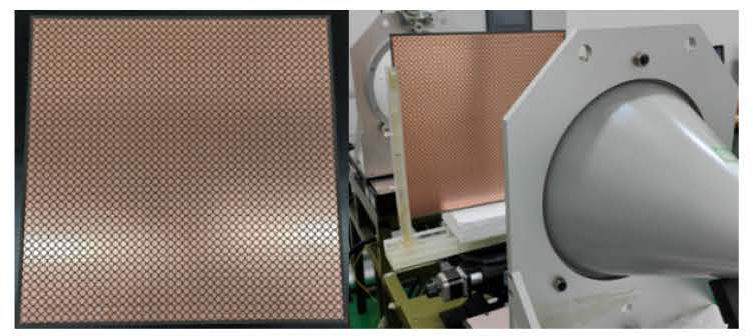
Figure 5: FSS sample and measurement setup.
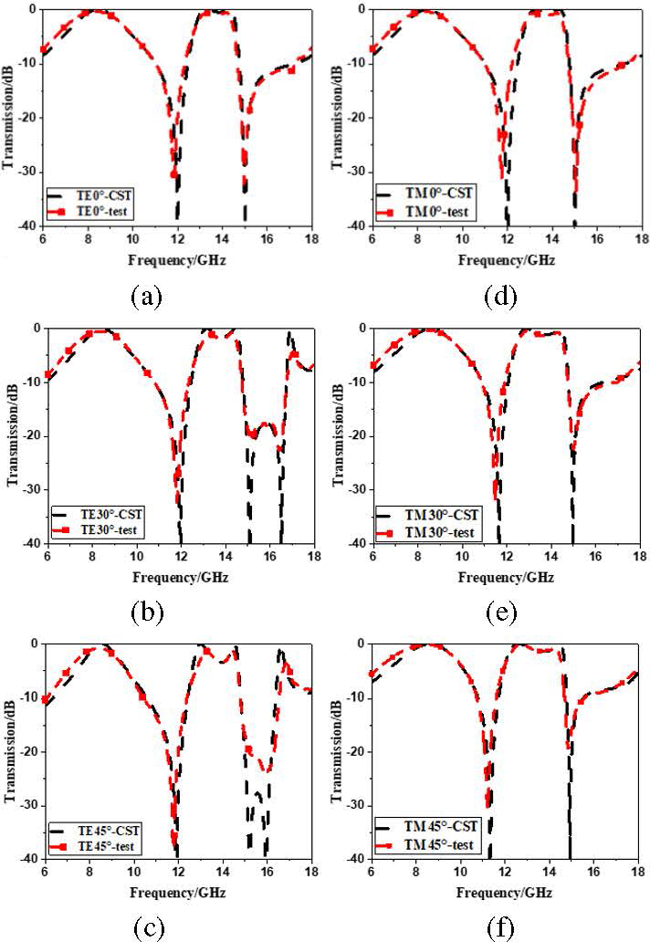
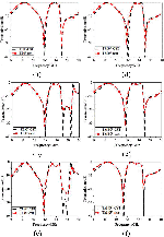
Figure 6: Measured transmission coefficients of the FSS sample under (a)-(c) TE polarization and (d)-(f) TM polarization.
To improve alignment accuracy, the top and middle layers were printed on both sides of the substrate. The bottom layer was printed on one side of another substrate. Meanwhile, five asymmetric location holes were drawn on the four edges of each board. They were used to improve alignment accuracy when the two boards are bonded together by a layer of EVA glue with a thickness of 0.045 mm, a dielectric constant of 3, and a loss tangent of 0.005. Hence, the physical dimensions of the prototype are 405 mm 405 mm 0.553 mm (0.015).
The free space measurement technique was used to measure S. An Agilent N5224A vector analyzer and three pairs of horn antennas covering 6-18 GHz were used to measure the proposed prototype. The experimental setup and the fabricated FSS prototype are shown in Fig. 5.
The performance of the proposed FSS has been verified experimentally under oblique incident wave. The measured and simulated transmission coefficients are plotted, derived from the simulation in Figs. 6 (a-d). They show good agreement with the simulated ones. There is a slight downshift for the lower transmission null whose maximum deviation is 0.25 GHz compared with simulation. The lower passband, whose maximum deviation of -3 dB bandwidth is 0.3 GHz, is a little broader than the simulated one. The deviations may be caused by a machining error of ACP and an alignment error between the two boards during bonding.
V. CONCLUSION
In this paper, a new dual-band FSS structure with low-profile and high selectivity at upper passband is presented. The segmental study method and equivalent circuit approach is used to establish its ECM and analyze its filtering mechanism. Two parallel LC resonators are responsible for the lower passband, whereas two hybrid LC resonators are series inductively coupled via L at the higher passband. A prototype of the proposed dual-band FSS has been fabricated and its performance has been verified through experiment. The proposed low-profile FSS with high selectivity has potential applications in designing low-frequency devices for dual-band communication.
ACKNOWLEDGMENT
The authors would like to acknowledge the support of Natural Science Foundation of Jilin Province, China (Grant No. YDZJ202301ZYTS378) and the Science and Technology Project of the Education Department of Jilin Province, China (Grant No. JJKH20230903KJ).
REFERENCES
[1] P. Jha, A. Kumar, A. De, and R. K. Jain, “Super ultra-wideband planar antenna with parasitic notch and frequency selective surface for gain enhancement,” Applied Computational Electromagnetics Society (ACES) Journal, vol. 37, no. 7, pp. 757-764, Dec. 2022.
[2] H. Ahmad, M. Rahman, S. Bashir, W. Zaman, and F. C. Seman, “Miniaturized frequency selective radome operating in the X-band with wideband absorption,” Applied Computational Electromagnetics Society (ACES) Journal, vol. 34, no. 12, pp. 1915-1921, Dec. 2019.
[3] Ş. Balta and M. Kartal, “A novel double-layer low-profile multiband frequency selective surface for 4G mobile communication system,” Applied Computational Electromagnetics Society (ACES) Journal, vol. 37, no. 4, pp. 420-427, Apr. 2022.
[4] M. Idrees, S. Buzdar, S. Khalid, and M. A. Khalid, “A miniaturized polarization independent frequency selective surface with stepped profile for shielding applications,” Applied Computational Electromagnetics Society (ACES) Journal, vol. 31, no. 5, pp. 531-536, Aug. 2021.
[5] M. S. Samani, R. S. Shirazi, and G. Moradi, “Multi-band frequency selective surface design based on idea of clusters in cellular communication systems,” Applied Computational Electromagnetics Society (ACES) Journal, vol. 30, no. 10, pp. 1079-1082, Aug. 2021.
[6] E. C. Braz and A. L. P. S. Campos, “A new multifractal geometry for design of frequency selective surfaces with dual band response,” Applied Computational Electromagnetics Society (ACES) Journal, vol. 30, no. 7, pp. 799-803, Aug. 2021.
[7] Z. Yu, X. Yang, W. Tang, J. Zhu, and C. Wang, “Three-dimensional dual-band frequency selective surface with close band spacing,” in CSQRWC Conference, Taiyuan, China, pp. 1-3, 2019.
[8] P. Jiang, W. Jiang, W. Hu, and S. Gong, “An interlaced grid dual-band dual-polarized bandpass FSS with a large band ratio,” IEEE Antennas Wireless Propag. Lett., vol. 21, no. 5, pp. 1027-1031, May 2022.
[9] Y.-H. Ma, D.-W. Wang, Y. Yu, and W.-S. Zhao, “Design of dual-band frequency-selective surfaces with independent tunability,” IEEE Trans. Antennas Propag., vol. 70, no. 12, pp. 12381-12386, Dec. 2022.
[10] A. Chatterjee, G. Ali Sarkar, and S. K. Parui, “A multi-layered frequency selective surface-based wireless filter with dual bandpass response,” in IEEE MTT-S Int. Microwave and RF Conference, Kolkata, India, pp. 1-4, 2018.
[11] X. Zhang, W. Wu, J. Huang, W. Zhang, Y. Ye, and N. Yuan, “Dual-polarized frequency selective rasorber with two transmission bands,” IEEE Access, vol. 7, pp. 139795-139801, Sep. 2019.
[12] B. Q. Hu, L. M. Zhan, C. Z. Chen, and W. G. Li, “Theoretical analysis and simulation of shape factor of bandpass filter,” Ship Electronic Engineering, vol. 39, no. 8, pp. 100-107, Aug. 2019.
[13] F. Costa, A. Monorchio, and G. Manara, “An overview of equivalent circuit modeling techniques of frequency selective surfaces and metasurfaces,” Applied Computational Electromagnetics Society (ACES) Journal, vol. 29, no. 12, pp. 960-976, Aug. 2021.
[14] D. Li, T. W. Li, R. Hao, H. S. Chen, W. Y. Yin, H. C. Yu, and E. P. Li, “A low-profile broadband bandpass frequency selective surface with two rapid band edges for 5G near-field applications,” IEEE Trans. Electromagnetic Compatibility, vol. 59, no. 2, pp. 670-676, Apr. 2017.
[15] M. Hussein, J. Zhou, Y. Huang, and B. Al-Juboori, “A low-profile miniaturized second-order bandpass frequency selective surface,” IEEE Antennas Wireless Propag. Lett., vol. 16, pp. 2791-2794, Aug. 2017.
[16] M. Al-Joumayly and N. Behdad, “A new technique for design of low-profile, second-order, bandpass frequency selective surfaces,” IEEE Trans. Antennas Propagat., vol. 57, no. 2, pp. 452-459, Feb. 2009.
BIOGRAPHIES

Jian Jiao received the Ph.D. degree in Optics from Changchun Institute of Optics, Fine Mechanics and Physics, Chinese Academy of Sciences, China, in 2015. She joined the School of Physics, Changchun Normal University, China, in 2019. Her research interests include frequency selective surface and artificial electromagnetic material.

Nianxi Xu received the Ph.D. degree in Optics from Changchun Institute of Optics, Fine Mechanics and Physics, Chinese Academy of Sciences, China, in 2012. He joined Changchun Institute of Optics, Fine Mechanics and Physics, Chinese Academy of Sciences, in 2012. His research interests include frequency selective surfaces and functional thin films.

Jinsong Gao received the Ph.D. degree in Optics from Changchun Institute of Optics, Fine Mechanics and Physics, Chinese Academy of Sciences, China, in 2005. He has been the director Jilin Provincial Key Laboratory of Advanced Optoelectronic Equipment and Instruments Manufacturing Technologies since 2017. His research interests include optical thin films, frequency selective surfaces, and functional thin films.
ACES JOURNAL, Vol. 39, No. 6, 548–554
doi: 10.13052/2024.ACES.J.390609
© 2024 River Publishers
